Background
Technical Field
The disclosure is related to liquid crystal display technology field, and more particular to a scan driving circuit for an oxide semiconductor thin film transistor and a NOR gate logic operation circuit thereof.
Related Art
For a large scale integrated circuit, three most basic elements in a logic operation circuit are an inverter, a NAND gate, or a NOR gate. Generally, the three elements are manufactured by using CMOS FET, i.e. the circuit includes two elements of PMOS and NMOS.
In an oxide semiconductor element, IGZO has become the focus of attention for the next generation display, and the oxide semiconductor has better NTFT characteristic due to the special material structure. However, the thin film transistor (TFT) also has two elements of PTFT and NTFT, but only in LTPS process, a PTFT element with better performance is obtained. Therefore, how to use a single element (PTFT or NTFT) to manufacture an inverter, a NAND or a NOR has become a serious problem.
Summary
The technique problem mainly solved by the disclosure is to provide a scan driving circuit for an oxide semiconductor thin film transistor and a NOR gate logic operation circuit thereof which is able to manufacture NAND by using a single element (PTFT or NTFT).
In order to solve the above technique problem, the disclosure provides NOR gate logic operation circuit, wherein the NOR gate logic operation circuit comprises a first invertor and a second invertor applied in a pull down holding circuit of a GOA circuit; a thirteenth transistor, a gate of the thirteenth transistor electrically connected to an output terminal of the first invertor, a drain of the thirteenth transistor electrically connected to a high potential of a constant voltage; a fourteenth transistor, a gate of the fourteenth transistor electrically connected to an output terminal of the second invertor, a drain of the fourteenth transistor electrically connected to a source of the thirteenth transistor, a source of the fourteenth transistor electrically connected to an output terminal of the logic operation circuit; a fifteenth transistor, a gate of the fifteenth transistor electrically connected to a first input terminal of the logic operation circuit, a drain of the fifteenth transistor electrically connected to the output terminal of the logic operation circuit, a source of the fifteenth transistor electrically connected to a low potential of the constant voltage; and a sixteenth transistor, a gate of the sixteenth transistor electrically connected to a second input terminal of the logic operation circuit, a drain of the sixteenth transistor electrically connected to the output terminal of the logic operation circuit, a source of sixteenth transistor electrically connected to the low potential of the constant voltage; the first invertor and the second invertor receive a circuit control signal through the low potential of the constant voltage and a first negative potential.
In order to solve the above technique problem, the disclosure further provides a NOR gate logic operation circuit, wherein the NOR gate logic operation circuit comprises a first invertor and a second invertor applied in a pull down holding circuit of a GOA circuit, a thirteenth transistor, a gate of the thirteenth transistor electrically connected to an output terminal of the first invertor, a drain of the thirteenth transistor electrically connected to a high potential of a constant voltage; a fourteenth transistor, a gate of the fourteenth transistor electrically connected to an output terminal of the second invertor, a drain of the fourteenth transistor electrically connected to a source of the thirteenth transistor, a source of the fourteenth transistor electrically connected to an output terminal of the logic operation circuit; a fifteenth transistor, a gate of the fifteenth transistor electrically connected to a first input terminal of the logic operation circuit, a drain of the fifteenth transistor electrically connected to the output terminal of the logic operation circuit, a source of the fifteenth transistor electrically connected to a low potential of the constant voltage; and a sixteenth transistor, a gate of the sixteenth transistor electrically connected to a second input terminal of the logic operation circuit, a drain of the sixteenth transistor electrically connected to the output terminal of the logic operation circuit, a source of sixteenth transistor electrically connected to the low potential of the constant voltage.
In one embodiment, the first invertor and the second invertor are the same, and each of the first invertor and the second invertor includes: a first transistor, a gate and a drain of the first transistor electrically connected to the high potential of the constant voltage, a source of the first transistor electrically connected to a first node; a second transistor, a gate of the second transistor electrically connected to the input terminal of the invertor, a drain of the second transistor electrically connected to the first node, a drain of the second transistor electrically connected to a first negative potential, a third transistor, a gate of the third transistor electrically connected to the first node, a drain of the third transistor electrically connected to the high potential of the constant voltage, a source of the third transistor electrically connected to the output terminal, a fourth transistor, a gate of the fourth transistor electrically connected to the input terminal of the invertor, a drain of the fourth transistor eclectically connected to the output terminal of the invertor, a source of the fourth transistor electrically connected to a second node; a fifth transistor, a gate and a drain of the fifth transistor electrically connected to the high potential of the constant voltage, a source of the fifth transistor electrically connected to a third node; a sixth transistor, a gate of the sixth transistor electrically connected to the input terminal of the invertor, a drain of the sixth transistor electrically connected to the third node, a source of the sixth transistor electrically connected to the low potential of the constant voltage; a seventh transistor, a gate of the seventh transistor electrically connected to the third node, a drain of the seventh transistor electrically connected to the high potential of the constant voltage, a source of the seventh transistor electrically connected to the second node; a eighth transistor, a gate of the eighth transistor electrically connected to the input terminal of the invertor, a drain of the eighth transistor electrically connected to second node, a source of the eighth transistor electrically connected to the low potential of the constant voltage.
In one embodiment, the first invertor and the second invertor receive a circuit control signal through the low potential of the constant voltage and the first negative potential.
In one embodiment, the first invertor and the second invertor are the same, and each of the first invertor and the second invertor includes: a twenty-first transistor, a gate and a drain of the twenty-first transistor electrically connected to the high potential of the constant voltage, a source of the twenty-first transistor electrically connected to a first node; a twenty-second transistor, a gate of the twenty-second transistor electrically connected to the input terminal of the invertor, a drain of the twenty-second transistor electrically connected to the first node, a drain of the twenty-second transistor electrically connected to a first negative potential; a twenty-third transistor, a gate of the twenty-third transistor electrically connected to the first node, a drain of the twenty-third transistor electrically connected to the high potential of the constant voltage, a source of the twenty-third transistor electrically connected to the output terminal of the invertor; a twenty-fourth transistor, a gate of the twenty-fourth transistor electrically connected to the input terminal of the invertor, a drain of the twenty-fourth transistor eclectically connected to the output terminal of the invertor, a source of the twenty-fourth transistor electrically connected to a second node; a twenty-fifth transistor, a gate of the twenty-fifth transistor electrically connected to a third node, a drain of the twenty-fifth transistor electrically connected to the high potential of the constant voltage, a source of the twenty-fifth transistor electrically connected to the second node; a twenty-sixth transistor, a gate of the twenty-sixth transistor electrically connected to the input terminal of the invertor, a drain of the twenty-sixth transistor electrically connected to the second node, a source of the twenty-sixth transistor electrically connected to the low potential of the constant voltage.
In one embodiment, the first invertor and the second invertor receive a circuit control signal through the high potential of the constant voltage and the low potential of the constant voltage.
In one embodiment the first invertor includes: a first transistor, a gate and a drain of the first transistor electrically connected to the high potential of the constant voltage, a source of the first transistor electrically connected to a first node; a second transistor, a gate of the second transistor electrically connected to the input terminal of the first invertor, a drain of the second transistor electrically connected to the first node, a drain of the second transistor electrically connected to a first negative potential; a third transistor, a gate of the third transistor electrically connected to the first node, a drain of the third transistor electrically connected to the high potential of the constant voltage, a source of the third transistor electrically connected to the output terminal; a fourth transistor, a gate of the fourth transistor electrically connected to the input terminal of the invertor, a drain of the fourth transistor eclectically connected to the output terminal of the first invertor, a source of the fourth transistor electrically connected to a second node; a fifth transistor, a gate and a drain of the fifth transistor electrically connected to the high potential of the constant voltage, a source of the fifth transistor is electrically connected to a third node; a sixth transistor, a gate of the sixth transistor electrically connected to the input terminal of the first invertor, a drain of the sixth transistor electrically connected to the third node, a source of the sixth transistor electrically connected to the low potential of the constant voltage; a seventh transistor, a gate of the seventh transistor electrically connected to the third node, a drain of the seventh transistor electrically connected to the high potential of the constant voltage, a source of the seventh transistor electrically connected to the second node; a eighth transistor, a gate of the eighth transistor electrically connected to the input terminal of the first invertor, a drain of the eighth transistor electrically connected to second node, a source of the eighth transistor electrically connected to the low potential of the constant voltage; the second invertor includes: a twenty-first transistor, a gate and a drain of the twenty-first transistor electrically connected to the high potential of the constant voltage, a source of the twenty-first transistor electrically connected to the first node; a twenty-second transistor, a gate of the twenty-second transistor electrically connected to the input terminal of the second invertor, a drain of the twenty-second transistor electrically connected to the first node, a drain of the twenty-second transistor electrically connected to the first negative potential; a twenty-third transistor, a gate of the twenty-third transistor electrically connected to the first node, a drain of the twenty-third transistor electrically connected to the high potential of the constant voltage, a source of the twenty-third transistor electrically connected to the output terminal of the second invertor, a twenty-fourth transistor, a gate of the twenty-fourth transistor electrically connected to the input terminal of the second invertor, a drain of the twenty-fourth transistor eclectically connected to the output terminal of the second invertor, a source of the twenty-fourth transistor electrically connected to the second node; a twenty-fifth transistor, a gate of the twenty-fifth transistor electrically connected to the third node, a drain of the twenty-fifth transistor electrically connected to the high potential of the constant voltage, a source of the twenty-fifth transistor electrically connected to the second node; a twenty-sixth transistor, a gate of the twenty-sixth transistor electrically connected to the input terminal of the second invertor, a drain of the twenty-sixth transistor electrically connected to the second node, a source of the twenty-sixth transistor electrically connected to the low potential of the constant voltage.
In one embodiment, the first invertor receives a circuit control signal through the low potential of the constant voltage and the first negative potential, and the second invertor receives the circuit control signal through the high potential of the constant voltage and the low potential of the constant voltage.
In one embodiment, a relationship of the first negative potential, a second negative potential and the low potential of the constant voltage is: the low potential of the constant voltage<the second negative potential<the first negative potential.
In one embodiment, the NOR gate logic operation circuit receives a circuit control signal through the high potential of the constant voltage and the low potential of the constant voltage.
In order to solve the above technique problem, the disclosure further provides a scan driving circuit for an oxide semiconductor thin film transistor, wherein the scan driving circuit comprises a NOR gate logic operation circuit, the NOR gate logic operation circuit comprising a first invertor and a second invertor applied in a pull down holding circuit of a GOA circuit, a thirteenth transistor, a gate of the thirteenth transistor electrically connected to an output terminal of the first invertor, a drain of the thirteenth transistor electrically connected to a high potential of a constant voltage; a fourteenth transistor, a gate of the fourteenth transistor electrically connected to an output terminal of the second invertor, a drain of the fourteenth transistor electrically connected to a source of the thirteenth transistor, a source of the fourteenth transistor electrically connected to an output terminal of the logic operation circuit; a fifteenth transistor, a gate of the fifteenth transistor electrically connected to a first input terminal of the logic operation circuit, a drain of the fifteenth transistor electrically connected to the output terminal of the logic operation circuit, a source of the fifteenth transistor electrically connected to a low potential of the constant voltage; a sixteenth transistor, a gate of the sixteenth transistor electrically connected to a second input terminal of the logic operation circuit, a drain of the sixteenth transistor electrically connected to the output terminal of the logic operation circuit, a source of sixteenth transistor electrically connected to the low potential of the constant voltage.
In one embodiment, the first invertor and the second invertor are the same, and each of the first invertor and the second invertor includes: a first transistor, a gate and a drain of the first transistor electrically connected to the high potential of the constant voltage, a source of the first transistor electrically connected to a first node; a second transistor, a gate of the second transistor electrically connected to the input terminal of the invertor, a drain of the second transistor electrically connected to the first node, a drain of the second transistor electrically connected to a first negative potential; a third transistor, a gate of the third transistor is electrically connected to the first node, a drain of the third transistor electrically connected to the high potential of the constant voltage, a source of the third transistor electrically connected to the output terminal; a fourth transistor, a gate of the fourth transistor electrically connected to the input terminal of the invertor, a drain of the fourth transistor eclectically connected to the output terminal of the invertor, a source of the fourth transistor electrically connected to a second node; a fifth transistor, a gate and a drain of the fifth transistor are electrically connected to the high potential of the constant voltage, a source of the fifth transistor electrically connected to a third node; a sixth transistor, a gate of the sixth transistor electrically connected to the input terminal of the invertor, a drain of the sixth transistor electrically connected to the third node, a source of the sixth transistor electrically connected to the low potential of the constant voltage; a seventh transistor, a gate of the seventh transistor electrically connected to the third node, a drain of the seventh transistor electrically connected to the high potential of the constant voltage, a source of the seventh transistor electrically connected to the second node; a eighth transistor, a gate of the eighth transistor electrically connected to the input terminal of the invertor, a drain of the eighth transistor electrically connected to second node, a source of the eighth transistor electrically connected to the low potential of the constant voltage.
In one embodiment, the first invertor and the second invertor receive a circuit control signal through the low potential of the constant voltage and the first negative potential.
In one embodiment, the first invertor and the second invertor are the same, and each of the first invertor and the second invertor includes: a twenty-first transistor, a gate and a drain of the twenty-first transistor electrically connected to the high potential of the constant voltage, a source of the twenty-first transistor electrically connected to a first node; a twenty-second transistor, a gate of the twenty-second transistor electrically connected to the input terminal of the invertor, a drain of the twenty-second transistor electrically connected to the first node, a drain of the twenty-second transistor electrically connected to a first negative potential; a twenty-third transistor, a gate of the twenty-third transistor electrically connected to the first node, a drain of the twenty-third transistor electrically connected to the high potential of the constant voltage, a source of the twenty-third transistor electrically connected to the output terminal of the invertor; a twenty-fourth transistor, a gate of the twenty-fourth transistor electrically connected to the input terminal of the invertor, a drain of the twenty-fourth transistor eclectically connected to the output terminal of the invertor, a source of the twenty-fourth transistor electrically connected to a second node; a twenty-fifth transistor, a gate of the twenty-fifth transistor electrically connected to a third node, a drain of the twenty-fifth transistor electrically connected to the high potential of the constant voltage, a source of the twenty-fifth transistor electrically connected to the second node; a twenty-sixth transistor, a gate of the twenty-sixth transistor electrically connected to the input terminal of the invertor, a drain of the twenty-sixth transistor electrically connected to the second node, a source of the twenty-sixth transistor electrically connected to the low potential of the constant voltage.
In one embodiment, the first invertor and the second invertor receive a circuit control signal through the high potential of the constant voltage and the low potential of the constant voltage.
In one embodiment, the first invertor includes: a first transistor, a gate and a drain of the first transistor electrically connected to the high potential of the constant voltage, a source of the first transistor electrically connected to a first node; a second transistor, a gate of the second transistor electrically connected to the input terminal of the first invertor, a drain of the second transistor electrically connected to the first node, a drain of the second transistor electrically connected to a first negative potential; a third transistor, a gate of the third transistor electrically connected to the first node, a drain of the third transistor electrically connected to the high potential of the constant voltage, a source of the third transistor electrically connected to the output terminal; a fourth transistor, a gate of the fourth transistor electrically connected to the input terminal of the invertor, a drain of the fourth transistor eclectically connected to the output terminal of the first invertor, a source of the fourth transistor electrically connected to a second node; a fifth transistor, a gate and a drain of the fifth transistor electrically connected to the high potential of the constant voltage, a source of the fifth transistor electrically connected to a third node; a sixth transistor, a gate of the sixth transistor electrically connected to the input terminal of the first invertor, a drain of the sixth transistor electrically connected to the third node, a source of the sixth transistor electrically connected to the low potential of the constant voltage; a seventh transistor, a gate of the seventh transistor electrically connected to the third node, a drain of the seventh transistor electrically connected to the high potential of the constant voltage, a source of the seventh transistor electrically connected to the second node; a eighth transistor, a gate of the eighth transistor electrically connected to the input terminal of the first invertor, a drain of the eighth transistor electrically connected to second node, a source of the eighth transistor electrically connected to the low potential of the constant voltage; the second invertor includes: a twenty-first transistor, a gate and a drain of the twenty-first transistor electrically connected to the high potential of the constant voltage, a source of the twenty-first transistor electrically connected to the first node; a twenty-second transistor, a gate of the twenty-second transistor electrically connected to the input terminal of the second invertor, a drain of the twenty-second transistor electrically connected to the first node, a drain of the twenty-second transistor electrically connected to the first negative potential; a twenty-third transistor, a gate of the twenty-third transistor electrically connected to the first node, a drain of the twenty-third transistor electrically connected to the high potential of the constant voltage, a source of the twenty-third transistor electrically connected to the output terminal of the second invertor; a twenty-fourth transistor, a gate of the twenty-fourth transistor electrically connected to the input terminal of the second invertor, a drain of the twenty-fourth transistor eclectically connected to the output terminal of the second invertor, a source of the twenty-fourth transistor electrically connected to the second node; a twenty-fifth transistor, a gate of the twenty-fifth transistor electrically connected to the third node, a drain of the twenty-fifth transistor electrically connected to the high potential of the constant voltage, a source of the twenty-fifth transistor is electrically connected to the second node; a twenty-sixth transistor, a gate of the twenty-sixth transistor electrically connected to the input terminal of the second invertor, a drain of the twenty-sixth transistor electrically connected to the second node, a source of the twenty-sixth transistor electrically connected to the low potential of the constant voltage.
In one embodiment, the first invertor receives a circuit control signal through the low potential of the constant voltage and the first negative potential, and the second invertor receives the circuit control signal through the high potential of the constant voltage and the low potential of the constant voltage.
In one embodiment, a relationship of the first negative potential, a second negative potential and the low potential of the constant voltage is: the low potential of the constant voltage<the second negative potential<the first negative potential.
In one embodiment, the NOR gate logic operation circuit receives a circuit control signal through the high potential of the constant voltage and the low potential of the constant voltage.
The effects of the disclosure different from the current technique is that the scan driving circuit for an oxide semiconductor thin film transistor and the NOR gate logic operation circuit thereof of the disclosure includes the first invertor and the second invertor applied in the pull down holding circuit of the GOA circuit, and a plurality of transistors. A combination of the NTFT and the invertor replaces the original function of an PMOS element to realize a characteristic similar to the original COMS NOR operation circuit, thereby solving a design problem of the logic operation circuit using a IGZO TFT single element, such that a larger scale digital integrated circuit further is suitably integrated into the liquid crystal display.
Brief description of the drawings
The above and other exemplary aspects, features and advantages of certain exemplary embodiments of the present disclosure will be more apparent from the following description taken in conjunction with the accompanying drawings, in which:
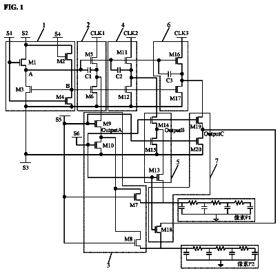
FIG. 1 is a circuit diagram of the NOR gate logic operation circuit according to the embodiment of the disclosure;
FIG. 2 is a circuit diagram of the first invertor of the NOR gate logic operation circuit according to the embodiment of the disclosure;
FIG. 3 a circuit diagram of the second invertor of the NOR gate logic operation circuit according to the embodiment of the disclosure.
Detailed description
The following description with reference to the accompanying drawings is provided to clearly and completely explain the exemplary embodiments of the disclosure. It is apparent that the following embodiments are merely some embodiments of the disclosure rather than all embodiments of the disclosure. According to the embodiments in the disclosure, all the other embodiments attainable by those skilled in the art without creative endeavor belong to the protection scope of the disclosure.
Refer to FIG. 1 . FIG. 1 is a circuit diagram of the NOR gate logic operation circuit according to the embodiment of the disclosure. The NOR gate logic operation circuit 10 is applied to a logic operation circuit of a scan driving circuit for an oxide semiconductor thin film transistor.
The circuit 10 includes a first invertor 100 and a second invertor 200 , wherein both of the first invertor 100 and the second invertor 200 are applied in a pull down holding circuit of a GOA circuit.
Further, both of the first invertor 100 and the second invertor 200 are applied in a mainly invertor portion of the pull down holding circuit of the GOA circuit.
The circuit 10 further includes:
a thirteenth transistor T 13 , a gate of the thirteenth transistor T 13 electrically connected to an output terminal of the first invertor, a drain of the thirteenth transistor T 13 electrically connected to a high potential of a constant voltage DCH;
a fourteenth transistor T 14 , a gate of the fourteenth transistor T 14 electrically connected to an output terminal of the second invertor, a drain of the fourteenth transistor T 14 electrically connected to a source of the thirteenth transistor T 13 , a source of the fourteenth transistor electrically connected to an output terminal Vout of the logic operation circuit;
a fifteenth transistor T 15 , a gate of the fifteenth transistor T 15 electrically connected to a first input terminal A of the logic operation circuit, a drain of the fifteenth transistor T 15 electrically connected to the output terminal Vout of the logic operation circuit, a source of the fifteenth transistor T 15 electrically connected to a low potential of the constant voltage DCL and
a sixteenth transistor T 16 , a gate of the sixteenth transistor T 16 electrically connected to a second input terminal B of the logic operation circuit, a drain of the sixteenth transistor T 16 electrically connected to the output terminal Vout of the logic operation circuit, a source of sixteenth transistor T 16 electrically connected to the low potential of the constant voltage DCL.
In one embodiment, the NOR gate logic operation circuit receives a circuit control signal through the high potential of the constant voltage DCH and the low potential of the constant voltage DCL.
Refer to FIG. 2 simultaneously. FIG. 2 is a circuit diagram of the first invertor of the NOR gate logic operation circuit according to the embodiment of the disclosure. The structure and the connection relationship of the invertor are described as following.
For the first transistor T 1 , a gate and a drain of the first transistor T 1 are electrically connected to the high potential of the constant voltage DCH, and a source of the first transistor T 1 is electrically connected to a first node S.
For the second transistor T 2 , a gate of the second transistor T 2 is electrically connected to the input terminal Vin of the invertor, a drain of the second transistor T 2 is electrically connected to the first node S, and a drain of the second transistor T 2 is electrically connected to a first negative potential VSS 1 .
For the third transistor T 3 , a gate of the third transistor T 3 is electrically connected to the first node S, a drain of the third transistor T 3 is electrically connected to the high potential of the constant voltage DCH, and a source of the third transistor T 3 is electrically connected to the output terminal Vout.
For the fourth transistor T 4 , a gate of the fourth transistor T 4 is electrically connected to the input terminal Vin of the invertor, a drain of the fourth transistor T 4 is eclectically connected to the output terminal Vout of the invertor, and a source of the fourth transistor T 4 is electrically connected to a second node K.
For the fifth transistor T 5 , a gate and a drain of the fifth transistor T 5 are electrically connected to the high potential of the constant voltage DCH, and a source of the fifth transistor T 5 is electrically connected to a third node M.
For the sixth transistor T 6 , a gate of the sixth transistor T 6 is electrically connected to the input terminal Vin of the invertor, a drain of the sixth transistor T 6 is electrically connected to the third node M, and a source of the sixth transistor T 6 is electrically connected to the low potential of the constant voltage DCL.
For the seventh transistor T 7 , a gate of the seventh transistor T 7 is electrically connected to the third node M, a drain of the seventh transistor T 7 is electrically connected to the high potential of the constant voltage DCH, and a source of the seventh transistor T 7 is electrically connected to the second node K.
For the eighth transistor T 8 , a gate of the eighth transistor T 8 is electrically connected to the input terminal Vin of the invertor, a drain of the eighth transistor T 8 is electrically connected to second node K, and a source of the eighth transistor T 8 is electrically connected to the low potential of the constant voltage DCL.
In one embodiment, the invertor receives a circuit control signal through the low potential of the constant voltage DCL and the first negative potential VSS 1 .
A relationship of the first negative potential VSS 1 , a second negative potential VSS 2 and the low potential of the constant voltage DCL is: the low potential of the constant voltage DCL<the second negative potential VSS 2 <the first negative potential VSS 1 .
FIG. 3 is a circuit diagram of the second invertor of the NOR gate logic operation circuit according to the embodiment of the disclosure. The structure and the connection relationship of the invertor are described as following:
For the twenty-first transistor T 21 , a gate and a drain of the twenty-first transistor T 21 are electrically connected to the high potential of the constant voltage DCH, and a source of the twenty-first transistor T 21 is electrically connected to the first node S.
For the twenty-second transistor T 22 , a gate of the twenty-second transistor T 22 is electrically connected to the input terminal Vin of the invertor, a drain of the twenty-second transistor T 22 is electrically connected to the first node S, and a drain of the twenty-second transistor T 22 is electrically connected to the first negative potential VSS 1 .
For the twenty-third transistor T 23 , a gate of the twenty-third transistor T 23 is electrically connected to the first node S, a drain of the twenty-third transistor T 23 is electrically connected to the high potential of the constant voltage DCH, and a source of the twenty-third transistor T 23 is electrically connected to the output terminal Vout of the invertor;
For the twenty-fourth transistor T 24 , a gate of the twenty-fourth transistor T 24 is electrically connected to the input terminal Vin of the invertor, a drain of the twenty-fourth transistor T 24 is eclectically connected to the output terminal Vout of the invertor, and a source of the twenty-fourth transistor T 24 is electrically connected to a second node K.
For the twenty-fifth transistor T 25 , a gate of the twenty-fifth transistor T 25 is electrically connected to the third node M, a drain of the twenty-fifth transistor T 25 is electrically connected to the high potential of the constant voltage DCH, and a source of the twenty-fifth transistor T 25 is electrically connected to the second node K.
For the twenty-sixth transistor T 26 , a gate of the twenty-sixth transistor T 26 is electrically connected to the input terminal Vin of the invertor, a drain of the twenty-sixth transistor T 26 is electrically connected to the second node K, and a source of the twenty-sixth transistor T 26 is electrically connected to the low potential of the constant voltage DCL.
In one embodiment, the invertor receives a circuit control signal through the low potential of the constant voltage DCL and the first negative potential VSS 1 .
A relationship of the first negative potential VSS 1 , a second negative potential VSS 2 and the low potential of the constant voltage DCL is: the low potential of the constant voltage DCL<the second negative potential VSS 2 <the first negative potential VSS 1 .
In the embodiment, both of the first invertor and the second invertor included in the circuit 100 are the invertor as shown in FIG. 2 .
In another embodiment, both of the first invertor and the second invertor included in the circuit 100 are the invertor as shown in FIG. 3 .
In yet another embodiment, the first invertor included in the circuit 100 is the invertor as shown in FIG. 2 , and the second invertor included in the circuit 100 is the invertor as shown in FIG. 3 .
According to the disclosure, the scan driving circuit for an oxide semiconductor thin film transistor and the NOR gate logic operation circuit thereof includes the first invertor and the second invertor applied in the pull down holding circuit of the GOA circuit, and a plurality of transistors. The combination of the NTFT and the invertor displaces the original function of the PMOS element to realize a characteristic similar to an original COMS NOR operation circuit, thereby solving a design problem of the logic operation circuit using a IGZO TFT single element, such that a larger scale digital integrated circuit is further suitably integrated into the liquid crystal display.
Although the present disclosure is illustrated and described with reference to specific embodiments, those skilled in the art will understand that many variations and modifications are readily attainable without departing from the spirit and scope thereof as defined by the appended claims and their legal equivalents.
 Lapsed, fee not paid8 drawings