Cross-reference to related application
This application claims the priority under 35 U.S.C. §119(a) to Korean Application Serial No. 10-2014-0100691, which was filed in the Korean Intellectual Property Office on Aug. 5, 2014, the entire content of which is hereby incorporated by reference.
Technical field
Various embodiments of the present disclosure relate to an antenna device.
Background
Recently, wireless communication techniques have been implemented by various methods, such as Wireless Local Area Network (W-LAN) represented by Wi-Fi technique, Bluetooth, and near field communication (NFC), in addition to commercial mobile communication network connection. Mobile communication services were initiated from a first generation mobile communication service centered on voice communication, and have gradually been developed to a super-high speed and large capacity service (e.g., a high quality video streaming service). It is expected that a next generation mobile communication service, which is to be commercially available in the future, will be provided through an ultra-high frequency band of dozens of GHz or more (hereinafter, the communication may be referred to as “mm-wave communication”).
The wavelength of a resonance frequency of an antenna device to be used for the mm-wave communication is in a mere range of 1 mm to 10 mm, and the size of a radiator may be further reduced. In addition, in the antenna device used for mm-wave communication, a Radio Frequency Integrated Circuit (RFIC) chip mounted with a communication circuit unit and a radiator may be arranged to be close to each other in order to suppress transmission loss occurring between the communication circuit and the radiator. Such an antenna device may be implemented in a modular form by arranging the RFIC chip and the radiator on a printed circuit board having a width and a length that do not exceed 30 mm, for example, a size of about 10 mm*25 mm.
In general, an operating frequency may be determined depending on the length of the radiator, and as the operating frequency band increases, the size of the antenna device, for example, the size of the radiator that performs a direct radiation operation of wireless signals may decrease. Assuming that a resonance frequency of the antenna device is λ, it means that the radiator may have an electric length of N*(λ/4). Here, N means a natural number. In a case where such an antenna device is mounted in a miniaturized, thinned, and light-weight electronic device, such as a mobile communication terminal, being under mounting space constraints is unavoidable. In particular, the antenna device is mounted within the electronic device in consideration of the radiation performance of the antenna device. Especially, in order to ensure a 360° coverage at the time of mm-wave communication, the antenna device is mounted on an edge portion, such as a corner portion of the circuit board. Since the electronic device have a very thin thickness as compared to the longitudinal size thereof, the antenna device mounted in the electronic device may be easily mounted in the longitudinal direction. That is, the radiator of the antenna device mounted in the electronic device may be easily formed to have a length corresponding to the frequency band in the longitudinal direction. Thus, a radiator having a polarized wave in the longitudinal direction (hereinafter, referred to as a “horizontally polarized wave”) may be easily mounted in an electronic device, may allow easy frequency design, and may have a good radiation efficiency. However, since the electronic device does not provide a sufficient length for allowing the mounting of the radiator of the antenna in the thickness direction of the electronic device, it is not easy to implement a polarized wave in the thickness direction (hereinafter, referred to as a “vertically polarized wave”) as well as to design a required frequency.
In addition, when a plurality of antenna modules are installed along the periphery of a board, a polarization loss occurs due to the interference between adjacent antenna modules. Thus, when the plurality of antenna modules are mounted, it is necessary for the antenna modules to be spaced apart from each other by a predetermined interval which unavoidably causes the integration of the antenna modules to be degraded.
Summary
Accordingly, various embodiments of the present disclosure are to provide an antenna device capable of securing various operating characteristics without being under mounting space restraints.
In addition, various embodiments of the present disclosure are to provide an antenna device capable of transmitting/receiving vertically polarized waves in a width direction having a very thin thickness as compared to a longitudinal direction as well as performing transmission/reception of horizontally polarized waves that are easily provided in the longitudinal direction of an electronic device.
Furthermore, various embodiments of the present disclosure are to provide an antenna device capable of minimizing the polarization loss even if antenna modules are provided to be close to each other, and improving the integration degree of antenna modules.
According to one embodiment among various embodiments of the present disclosure, an antenna device may include: a board unit; and a radiator arranged in a width direction along a periphery of the board unit to generate an electric field and a magnetic field in the width direction.
In addition, according to one embodiment among various embodiments of the present disclosure, an antenna device may include: a board unit; a power feeding unit provided in the board unit; and radiation units connected to the power feeding unit to be fed with a power feeding signal, the radiation units being provided to face each other within a width of the board unit along a periphery of the board unit.
In addition, according to one of various embodiments of the present disclosure, an antenna device may include: a board unit; a power feeding unit provided in the board unit; and first and second radiators connected to the power feeding unit to be provided with a power feeding signal, the first and second radiators being provided to face each other along a periphery of the board unit and within a width of the board unit. The first radiator may include a radiation patch connected with the power feeding unit and protruding in a longitudinal direction of the board unit, the second radiator may include first and second radiation patches spaced apart from the first radiator to face the first radiator parallel to the first radiator above and below the first radiator, and the first radiator and the second radiator may generate a vertical polarization radiation pattern.
In addition, according to one of various embodiments of the present disclosure, an antenna device may include: a board unit; a power feeding unit provided in the board unit; and first and second radiators connected to the power feeding unit to be provided with a power feeding signal, positioned on a peripheral surface of the board unit, and provided to face the peripheral surface of the board unit and face each other within a width of the board unit. The first radiator may include a column portion formed to be spaced apart from an end of the board unit and connected with the power feeding unit, and plates protruding from opposite ends of the column portion toward the board unit, the second radiator may include a plurality of radiation patches protruding toward the column portion along a width direction of the board unit, and the first radiator and the second radiator may generate a vertical polarization radiation pattern.
In addition, according to one of various embodiments of the present disclosure, an antenna device may include: a board unit; a power feeding unit provided in the board unit; radiation members connected to the power feeding unit to be provided with a power feeding signal, and provided to face each other along a periphery of the board unit and within a width of the board unit; and one or more guide radiation members provided in a direction away from the peripheral surface of the board unit, and arranged close to the radiation members. The radiation members may generate a vertical polarization radiation pattern, and the guide radiation member adjusts a directivity of the antenna device.
In addition, according to one of various embodiments of the present disclosure, an antenna device may include: a board unit; a power feeding unit provided in the board unit; and first and second radiation patches connected to the power feeding unit to be supplied with a power feeding signal, and provided to face each other along a periphery of the board unit and within a width of the board unit, the first and second radiation patches generating an electric field in a direction horizontal to the board unit and an electric field in a direction vertical to the board unit so as to generate a horizontal polarization antenna pattern and a vertical polarization antenna pattern.
Further, according to one of various embodiments of the present disclosure, an antenna device may include: a board unit; a power feeding unit provided in the board unit; and first and second radiators connected to the power feeding unit to be provided with a power feeding signal, positioned on a peripheral surface of the board unit, and provided to face the peripheral surface of the board unit and face each other within a width of the board unit. The power feeding unit may include a first power feeding line connected to the first radiator to provide a horizontal polarization power feeding signal between the first radiator and the second radiator, and a second power feeding line connected to the first radiator to provide a vertical polarization power feeding signal between the first radiator and the second radiator. At least one of a vertical polarization radiation pattern, a horizontal polarization radiation pattern, a diagonal polarization radiation pattern, and a circular polarization radiation pattern may be generated according to selective ON/OFF of the first and second power feeding lines.
According to various embodiments of the present disclosure, an antenna device according to present disclosure may be mounted within a mounting space that is narrow in width direction of an electronic device, such as a mobile communication terminal, to be capable of transmitting/receiving vertically polarized waves.
In connection with an operating frequency, it is possible to implement an antenna device capable of securing various operating characteristics without being restricted by a mounting space. For example, it is possible to implement an antenna device that enables the transmission/reception of vertically polarized waves by adjusting a horizontal length of an antenna, and enables transmission/reception of vertically polarized waves, transmission/reception of wideband circularly polarized waves and dual power feeding.
In addition, even if antenna devices are mounted close to each other along an edge of an electronic device, a polarization loss can be minimized and a mounting distance between an antenna module and a neighboring antenna device can be minimized, and the integration degree of antenna devices can be improved.
Brief description of the drawings
The above and other aspects, features, and advantages of the present disclosure will be more apparent from the following detailed description taken in conjunction with the accompanying drawings, in which:
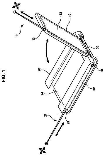
FIGS. 1A and 1B are views illustrating a radiation unit that has an open-stub structure in an antenna device according to one embodiment among various embodiments of the present disclosure;
FIGS. 2A to 2C are views illustrating a radiation unit that has a short-stub structure in the antenna device according to one embodiment among various embodiments of the present disclosure;
FIG. 3 is a sectional view schematically illustrating an antenna device according to a first embodiment among various embodiments of the present disclosure;
FIG. 4 is a perspective view schematically illustrating the antenna device according to the first embodiment among various embodiments of the present disclosure;
FIG. 5 is a view illustrating a vertical polarization radiation pattern generated in a radiation unit in the antenna device according to the first embodiment among various embodiments of the present disclosure;
FIG. 6 is a view illustrating a frequency change according to lengths of first and second radiation patches in the antenna device according to the first embodiment among various embodiments of the present disclosure;
FIG. 7 is a graph illustrating a reflection coefficient (S(1,1)) according to a difference in length between first and second radiation patches in the antenna device according to the first embodiment among various embodiments of the present disclosure;
FIG. 8 is a view illustrating a measured radiation characteristic of the antenna device according to the first embodiment among various embodiments of the present disclosure;
FIG. 9 is a view schematically illustrating an antenna device according to a second embodiment among various embodiments of the present disclosure;
FIG. 10 is a perspective view illustrating a state in which a radiation unit is mounted on a board unit in the antenna device according to the second embodiment among various embodiments of the present disclosure;
FIG. 11 is a view illustrating a frequency change according to a length of a radiation patch in the antenna device according to the second embodiment among various embodiments of the present disclosure;
FIG. 12 is a view illustrating a measured radiation characteristic of the antenna device according to the second embodiment among various embodiments of the present disclosure;
FIG. 13 is a view schematically illustrating an antenna device according to a third embodiment among various embodiments of the present disclosure;
FIG. 14 is a perspective view illustrating a state in which a radiation unit is mounted on a board unit in the antenna device according to the third embodiment among various embodiments of the present disclosure;
FIG. 15 is a graph illustrating a reflection coefficient (S(1,1)) of the antenna device according to the third embodiment among various embodiments of the present disclosure;
FIG. 16 is a view illustrating a radiation characteristic according to the number of guide radiation members in the antenna device according to the third embodiment among various embodiments of the present disclosure;
FIG. 17 is a view illustrating a radiation characteristic of the antenna device according to the third embodiment among various embodiments of the present disclosure;
FIG. 18 is a view schematically illustrating an antenna device according to a fourth embodiment among various embodiments of the present disclosure;
FIG. 19 is a perspective view illustrating a state in which a radiation unit is mounted on a board unit in the antenna device according to the fourth embodiment among various embodiments of the present disclosure;
FIGS. 20A and 20B are views illustrating electric fields of a vertical polarization radiation pattern and a horizontal polarization radiation pattern generated in first and second radiation patches of the antenna device according to the fourth embodiment among various embodiments of the present disclosure;
FIG. 21 is a graph illustrating a reflection coefficient (S(1,1)) of the antenna device according to the fourth embodiment among various embodiments of the present disclosure;
FIG. 22 is a graph illustrating a frequency band capable of being secured by first and second radiation patches in the antenna device according to the fourth embodiment among various embodiments of the present disclosure;
FIG. 23 is a view illustrating a measured radiation characteristic of the antenna device according to the fourth embodiment among various embodiments of the present disclosure;
FIG. 24 is a view schematically illustrating an antenna device according to a fifth embodiment among various embodiments of the present disclosure;
FIG. 25 is a perspective view illustrating a state in which a radiation unit is mounted on a board unit in the antenna device according to the fifth embodiment among various embodiments of the present disclosure;
FIG. 26 is a table illustrating radiation patterns according to selective ON/OFF of first and second power feeding lines in the antenna device according to the fifth embodiment among various embodiments of the present disclosure;
FIG. 27 is a graph illustrating a measured reflection coefficient (S(1,1)) of the antenna device according to the fifth embodiment among various embodiments of the present disclosure;
FIGS. 28A and 28B are views illustrating a radiation characteristic of the antenna device according to fifth embodiment among various embodiments of the present disclosure;
FIGS. 29A to 29C are views illustrating a case in which the antenna device according to the fifth embodiment among various embodiments of the present disclosure is provided with radiation units having two different frequency bands; and
FIGS. 30A to 30E are views illustrating a case in which the antenna device according to the fifth embodiment among various embodiments of the present disclosure is provided with two radiation units as transmission and reception patterns.
Detailed description
Hereinafter, various embodiments of the present disclosure will be described with reference to the accompanying drawings. The present disclosure may have various embodiments, and modifications and changes may be made therein. Therefore, the present disclosure will be described in detail with reference to particular embodiments shown in the accompanying drawings. However, it should be understood that there is no intent to limit various embodiments of the present disclosure to the particular embodiments disclosed herein, but the present disclosure should be construed to cover all modifications, equivalents, and/or alternatives falling within the spirit and scope of the various embodiments of the present disclosure. In the description of the drawings, identical or similar reference numerals are used to designate identical or similar elements.
As used in various embodiments of the present disclosure, the expressions “include”, “may include” and other conjugates refer to the existence of a corresponding disclosed function, operation, or constituent element, and do not limit one or more additional functions, operations, or constituent elements. Further, as used in various embodiments of the present disclosure, the terms “include”, “have”, and their conjugates are intended merely to denote a certain feature, numeral, step, operation, element, component, or a combination thereof, and should not be construed to initially exclude the existence of or a possibility of addition of one or more other features, numerals, steps, operations, elements, components, or combinations thereof.
Further, as used in various embodiments of the present disclosure, the expression “or” includes any or all combinations of words enumerated together. For example, the expression “A or B” may include A, may include B, or may include both A and B.
While expressions including ordinal numbers, such as “first” and “second”, as used in various embodiments of the present disclosure may modify various constituent elements, such constituent elements are not limited by the above expressions. For example, the above expressions do not limit the sequence and/or importance of the elements. The above expressions are used merely for the purpose of distinguishing an element from the other elements. For example, a first user device and a second user device indicate different user devices although both of them are user devices. For example, a first element may be termed a second element, and likewise a second element may also be termed a first element without departing from the scope of various embodiments of the present disclosure.
It should be noted that if it is described that an element is “coupled” or “connected” to another element, the first element may be directly coupled or connected to the second element, and a third element may be “coupled” or “connected” between the first and second elements. Conversely, when one component element is “directly coupled” or “directly connected” to another component element, it may be construed that a third component element does not exist between the first component element and the second component element.
The terms as used in various embodiments of the present disclosure are merely for the purpose of describing particular embodiments and are not intended to limit the various embodiments of the present disclosure. As used herein, the singular forms are intended to include the plural forms as well, unless the context clearly indicates otherwise.
Unless defined otherwise, all terms used herein, including technical terms and scientific terms, have the same meaning as commonly understood by a person of ordinary skill in the art to which various embodiments of the present disclosure pertain. Such terms as those defined in a generally used dictionary are to be interpreted to have the meanings equal to the contextual meanings in the relevant field of art, and are not to be interpreted to have ideal or excessively formal meanings unless clearly defined in various embodiments of the present disclosure.
An electronic device according to various embodiments of the present disclosure may be a device having a function that is provided through various colors emitted depending on the states of the electronic device or a function of sensing a gesture or bio-signal. For example, the electronic device may include at least one of a smart phone, a tablet personal computer (PC), a mobile phone, a video phone, an e-book reader, a desktop PC, a laptop PC, a netbook computer, a personal digital assistant (PDA), a portable multimedia player (PMP), an MP3 player, a mobile medical device, a camera, a wearable device (e.g., a head-mounted-device (HMD) such as electronic glasses, electronic clothes, an electronic bracelet, an electronic necklace, an electronic appcessory, an electronic tattoo, or a smart watch).
According to some embodiments, the electronic device may be a smart home appliance having a function serviced by light that emits various colors depending on the states of the electronic device or a function of sensing a gesture or bio-signal. The smart home appliance as an example of the electronic device may include at least one of, for example, a television, a Digital Video Disc (DVD) player, an audio, a refrigerator, an air conditioner, a vacuum cleaner, an oven, a microwave oven, a washing machine, an air cleaner, a set-top box, a TV box (e.g., Samsung HomeSync™, Apple TV™, or Google TV™), a game console, an electronic dictionary, an electronic key, a camcorder, and an electronic picture frame.
According to some embodiments, the electronic device may include at least one of various medical appliances (e.g., magnetic resonance angiography (MRA), magnetic resonance imaging (MRI), computed tomography (CT), and ultrasonic equipment), navigation equipment, a global positioning system (GPS) receiver, an event data recorder (EDR), a flight data recorder (FDR), automotive infotainment device, electronic equipment for ships (e.g., ship navigation equipment and a gyrocompass), avionics, security equipment, a vehicle head unit, an industrial or home robot, an automatic teller machine (ATM) of a banking system, and a point of sales (POS) of a shop.
According to some embodiments, the electronic device may include at least one of a part of furniture or a building/structure, an electronic board, an electronic signature receiving device, a projector, and various kinds of measuring instruments (e.g., a water meter, an electric meter, a gas meter, and a radio wave meter), each of which has a function that is provided through various colors emitted depending on the states of the electronic device or a function of sensing a gesture or bio-signal. The electronic device according to various embodiments of the present disclosure may be a combination of one or more of the aforementioned various devices. Further, the electronic device according to various embodiments of the present disclosure may be a flexible device. Further, it will be apparent to those skilled in the art that the electronic device according to various embodiments of the present disclosure is not limited to the aforementioned devices.
Hereinafter, an electronic device according to various embodiments of the present disclosure will be described with reference to the accompanying drawings. The term “user” as used in various embodiments of the present disclosure may refer to a person who uses an electronic device or a device (e.g., artificial intelligence electronic device) that uses an electronic device.
Hereinafter, a concept of an antenna device according to various embodiments of the present disclosure may be described with reference to FIGS. 1 and 2 , an antenna device according to a first embodiment among various embodiments of the present disclosure may be described with reference to FIGS. 3 to 8 , an antenna device according to a second embodiment among various embodiments of the present disclosure may be described with reference to FIGS. 9 to 12 , an antenna device according to a third embodiment among various embodiments of the present disclosure may be described with reference to FIGS. 13 to 17 , an antenna device according to a fourth embodiment among various embodiments of the present disclosure may be described with reference to FIGS. 18 to 23 , and an antenna device according to a fifth embodiment among various embodiments of the present disclosure may be described with reference to FIGS. 24 to 30 .
FIGS. 1A and 1B are views illustrating a radiation unit 20 that has an open-stub structure in an antenna device 10 according to one embodiment among various embodiments of the present disclosure, and FIGS. 2A to 2C are views illustrating a radiation unit 20 that has a short-stub structure in the antenna device 10 according to one embodiment among various embodiments of the present disclosure.
Referring to FIGS. 1A and 1B and FIGS. 2A to 2C , the antenna device 10 according to various embodiments of the present disclosure may include a board unit 11 , a power feeding unit 12 , and a radiation unit 20 .
The board unit 11 may be formed of, e.g., a flexible printed circuit board or a dielectric board, in which a plurality of layers are laminated. Each of the layers may include via holes formed or defined to penetrate a printed circuit pattern formed of a conductive material, a ground layer, or front and rear surfaces (or top and bottom surfaces) thereof.
In general, the via holes (not illustrated in FIGS. 1 and 2 ) formed in the multi-layered circuit board are formed for the purpose of electrical connection of printed circuit patterns formed in different layers or heat radiation. According to the embodiments of the present disclosure, the antenna device 10 may include via holes arranged in a grid form in a portion of the board unit 11 or portions spaced apart from each other in the board unit 11 and laminated to be connected with each other in a width direction so that the via holes may be utilized as a radiation member in the width direction (a “column portion” in the present disclosure may correspond to the radiation member and will be referred to as a “radiation column member 21 ” below).
In a certain embodiment, each of the layers forming the board unit 11 may include a plurality of via holes arranged in one direction (hereinafter, referred to as a “horizontal direction”) in some regions, for example, a region adjacent to an edge. When the respective layers are laminated to form the board unit 11 , via holes formed in one of the layers (first layer) may be aligned with the via holes formed in another layer (second layer) adjacent to the first layer. The via holes of the first layer and the via holes of the second layer may be arranged in straight lines. Between the via holes of the first layer and the via holes of the second layer, via pads may be arranged, respectively, so that a stable connection may be provided between each two via holes arranged in the different layers and adjacent to each other.
The radiation column member 21 is formed by via holes within or adjacent to the board unit 11 such that, for example, a radiator 23 or a radiation patch 22 to be described later is arranged in a direction vertical to the radiation column member 21 . Thus, the radiation column member 21 may be connected to a communication circuit unit or a ground unit GND even though, for example, a separate connection member is not disposed. That is, a power feeding line or a ground line of a power feeding unit 12 may be connected to the radiation column member 21 while the board unit 11 is fabricated.
The power feeding unit 12 may be connected to one of the via holes so as to provide power feeding signals from an RFIC chip 14 configured in the board unit 11 . In addition, some of the via holes or via pads that form the radiation column member 21 , for example, at least one via pad, may provide a ground to the radiation unit 20 so as to suppress the leakage of the power feeding signals. The power feeding unit 12 or the ground unit GND may be configured in a layer positioned on a surface of the board unit 11 .
Radiation units 20 may be provided along the periphery of the board unit 11 to be opposed to each other within the width of the board unit 11 and may be connected to the power feeding unit 12 to be provided with the power feeding signals. In particular, the radiation units 20 according to various embodiments of the present disclosure may be installed in the width direction having a very thin thickness as compared to the longitudinal size of the board unit 11 so as to implement a vertical polarization radiation pattern, and may have a cavity antenna structure. More specifically, according to, e.g., lamination or shape, the radiation units 20 may have an open-stub structure that is opened-opened. Otherwise, the radiation units 20 may have a short-stub structure that is opened-shorted.
More specifically, referring to FIGS. 1A and 1B , according to one embodiment among various embodiments of the present disclosure, the radiation unit 20 may include a radiator 23 and a plurality of radiation patches 22 to form an open stub structure. The radiation patches 22 may be formed to protrude in a direction (Y-axis direction) horizontal to the top and bottom surfaces of the board unit 11 at the opposite ends of the radiation column member 21 provided in the width direction (Z-axis direction) of the board unit 11 in a flat plate shape having a predetermined area. More specifically, the radiator 23 may be formed to be in point contact with the power feeding unit 12 , and to protrude in a direction perpendicular to a peripheral surface in the width between the top and bottom surfaces of the board unit 11 . In addition, the radiation patches 22 may be disposed on the top and bottom surfaces of the board unit 11 , respectively. That is, the radiator 23 may be provided between an upper radiation patch 22 and a lower radiation patch 22 having a predetermined width in the vertical direction at the top and bottom portions of the radiation column member 21 provided along the peripheral surface of the board unit 11 . Thus, the space between the upper radiation patch 22 and the radiator 23 is opened and the space between lower radiation patch 22 and the radiator 23 is opened, so that the radiation unit may have an open stub structure. At this time, the length of the radiation patches 22 may have an electric length of N*(λ/2). Here, N means a natural number and λ means a resonance frequency of the antenna device 10 . When a current is applied to the antenna device 10 having such a structure, a vertical electric field may be generated from the radiation patches 22 and radiated from the opened regions so that the antenna device 10 may have a horizontal radiation characteristic.
Referring to FIGS. 2A to 2C , according to one embodiment among various embodiments of the present disclosure, a radiation unit 20 may include radiation patches 22 arranged to face each other on a radiation column member 21 so as to form a short stub structure. More specifically, as illustrated in FIG. 2A , two radiation patches 22 may be disposed within the width of a board unit 11 , more specifically at the opposite ends of the radiation column member 21 to face each other. In addition, as illustrated in FIG. 2B or 2C , the upper and lower radiation patches 22 may be provided such that one of the radiation patches 22 is formed as if it is bent by a radiator 23 extending an end thereof to be close to and face another radiation patch 22 . Thus, the radiation unit 20 may have an open-short stub structure, in which one ends of the upper radiation patch 22 and the lower radiation patch 22 are shorted and the other ends thereof are opened. At this time, the radiation patches 22 may have an electric length of N*(λ/4). Here, N means a natural number and λ means a resonance frequency of the antenna device 10 . When a current applied to the antenna device 10 having such a structure, a vertical electric field may be generated between the radiation patches 22 and radiated in the opened region so that the antenna device may have a horizontal radiation characteristic.
Hereinafter, an antenna device 100 according to a first embodiment will be described with reference to FIGS. 3 to 8 .
FIG. 3 is a sectional view schematically illustrating an antenna device 100 a according to the first embodiment among various embodiments of the present disclosure. FIG. 4 is a perspective view schematically illustrating the antenna device 100 a according to the first embodiment among various embodiments of the present disclosure. FIG. 5 is a view illustrating a vertical polarization radiation pattern generated in a radiation unit 200 a in the antenna device 100 a according to the first embodiment among various embodiments of the present disclosure.
Referring to FIGS. 3 to 5 , the antenna device according to the first embodiment has the same configuration as the antenna device illustrated in FIG. 1A described above, and corresponds to an embodiment of an open stub structure among the antenna devices of the present disclosure.
As described above, the antenna device 100 a according to the first embodiment may include a board unit 110 a , a power feeding unit 120 a , and a radiation unit 200 a.
The board unit 110 a may be formed of a multi-layered circuit board having a plurality of laminated layers. The multi-layered circuit board may include a plurality of via holes 111 a . The via holes 111 a may be provided in order to electrically connect printed circuit boards formed on different layers, or for the purpose of heat radiation. The via holes 111 a may also be formed to penetrate a ground layer, a front surface (or a top surface), and a rear surface (or a bottom surface) of the multi-layered circuit board.
The radiation unit 200 a may be provided with power feeding signals from an RFIC chip 140 a via the power feeding unit 120 a . The radiation unit 200 a may be positioned on a peripheral surface of the board unit 110 a , and may include a first radiator 230 a and a second radiator 220 a that are disposed to face each other, and that may be in parallel to each other within the width of the board unit 110 a.
The first radiator 230 a is connected with the power feeding unit 120 a , and may be provided as a radiation patch 230 a protruding while having a predetermined area in a direction (Y-axis direction) horizontal to the length of the board unit 110 a (having an area in the X-Y plane direction). As described above, the radiation patch 230 a according to the first embodiment may have a predetermined area in the longitudinal direction of the board unit 110 a on the peripheral surface of the board unit 110 a . In addition, the radiation patch (the first radiator) 230 a may be placed between a first radiation patch 221 a and a second radiation patch 222 a (of the second radiator 220 a ) to be described later. As the radiation patch 230 a is disposed between the first radiation patch 221 a and the second radiation patch 222 a as described above, the radiation unit 200 may have the open stub structure described above.
The second radiator 220 a may be provided to have an open stub structure to face the radiation patch 230 a . More specifically, the radiator 220 a may include the first radiation patch 221 a and the second radiation patch 222 a which may be provided on the top and bottom surfaces of the board unit 110 a to be spaced apart from each other by the width of the board unit and to face each other. The first radiation patch 221 a and the second radiation patch 222 a may be disposed such that the first radiator 230 a is interposed therebetween and the first radiation patch 221 a and the second radiation patch 222 a are parallel to the top and bottom surfaces of the first radiator 230 a , respectively. The first radiation patch 221 a and the second radiation patch 222 a are electrically connected with each other via a radiation column member 210 a formed by the via holes 111 a laminated in multiple layers in the width direction of the board unit 110 a to be connected with each other.
When power feeding signals are applied through the power feeding unit 120 a , the first radiation patch 221 a may generate a first electric field in a direction vertical to a first surface of the first radiation patch 221 a , and the second radiation patch 222 a may generate a second electric field in a direction vertical to a second surface of the second radiation patch 222 a . Accordingly, a vertically polarized wave may be generated according to the vertical electric field generated between the first radiation patch 221 a and the first radiator 230 a , and according to the vertical electric field generated between the second radiation patch 222 a and the first radiator 230 a . A horizontal radiation characteristic may also be provided through the open regions between the first radiation patch 221 a and the radiation patch 230 a , and between the second radiation patch 222 a and the radiation patch 230 a.
FIG. 6 is a view illustrating a frequency change according to lengths of the first radiation patch 221 a and the second radiation patch 222 a in the antenna device 100 a according to the first embodiment among various embodiments of the present disclosure. FIG. 7 is a graph illustrating a reflection coefficient (S(1,1)) according to a difference in length between the first radiation patch 221 a and the second radiation patch 222 a in the antenna device 100 a according to the first embodiment among various embodiments of the present disclosure. FIG. 8 is a view illustrating a measured radiation characteristic of the antenna device 100 a according to the first embodiment among various embodiments of the present disclosure.
The description continues in the full USPTO document.
 Lapsed, fee not paid13 drawings

