Field of the invention
The field of this invention is the apparatus, composition, and fabrication of lithium-based, solid-state, thin-film, secondary and primary batteries with improved capacity density, energy density, and power density, and preferably with flexible form factor and crystalline LiCoO.sub.2, LiNiO.sub.2, LiMn.sub.2O.sub.4 cathodes and derivative materials.
Background of the invention
The following passage describes the need and evolution of the subject technology in the field of thin film batteries.
Thin-film batteries may be fabricated by sequential vacuum depositions of layered battery components onto a given substrate in, for example, the following order: positive cathode current collector, positive cathode, negative anode current collector, electrolyte (separator), negative anode, and encapsulation. A lamination process may be used instead of a deposition process step (see, for example, U.S. Pat. No. 6,916,679 versus Wang et al., 143 J. Electrochem. Soc. 3203-13
or U.S. Pat. No. 5,561,004). Optionally, the two terminals of a thin-film battery may not simply comprise extensions of the positive and the negative current collectors, but may be additionally deposited terminal contacts that make electrical contact to the respective current collector. The positive cathode material may be insufficiently crystalline in the as-deposited state and, associated with this fact, may exhibit insufficient electrochemical properties (see, for example, Wang et al., supra). For this reason, the positive cathode may be crystallized during battery fabrication, which can be achieved in a post-deposition, high-temperature (“anneal”) process (see, for example, Wang et al., supra or Bates et al., “Thin-Film Lithium Batteries” in New Trends in Electrochemical Technology: Energy Storage Systems for Electronics (T. Osaka & M. Datta eds., Gordon and Breach 2000)). The anneal process, which is applied immediately after the deposition of the positive cathode, may limit the choice of materials for the substrate and positive cathode current collector, thereby limiting, in turn, the capacity density, energy density, and power density of the thin-film battery, both per volume and weight. The affect of the substrate on those three quantities is, for example, explained in more detail below.
The intrinsic (i.e., without substrate and without encapsulation) volumetric and gravimetric densities of the capacity, the energy, and the power of lithium-based, solid-state, thin-film secondary (rechargeable) and primary (non-rechargeable) batteries are dominated by the volumetric and gravimetric densities of the capacity, the energy, and the power of the positive cathode material. Crystalline LiCoO.sub.2 may be an example of a choice for the positive cathode material for both bulk (non thin-film) and thin-film batteries in terms of volumetric and gravimetric densities of the capacity, energy, power, and cyclability, in the case of secondary batteries, followed by derivatives of crystalline LiMn.sub.2O.sub.4, crystalline LiMnO.sub.2, and crystalline LiNiO.sub.2. Doping these main parent positive cathode materials with other transition metals (leading to derivatives) such as Sc, Ti, V, Cr, Mn, Fe, Co, Ni, Cu, Zn, Y, Zr, Nb, Mo, Ru, Rh, La, Hf, Ta, W, and Re and main group elements selected from the groups 1, 2, 13, 14, 15, 16 and 17 has been found to alter the properties of LiCoO.sub.2, LiMn.sub.2O.sub.4, LiMnO.sub.2, and LiNiO.sub.2 with only little, if any, overall improvement.
According to U.S. Pat. No. 6,280,875, native titanium oxide on a Ti substrate is not inert enough to prevent adverse reactions from occurring between a Ti substrate and the battery components. This approach is severely restricted because the choice of substrate materials is limited to materials capable of forming a native surface oxide during the anneal step of the positive cathode. Apart from the present invention, metallic substrates including flexible foils that do not form a native surface oxide have not been employed successfully as thin-film battery substrates. Fabricating solid-state, thin-film secondary batteries by depositing, for example, high-temperature cathode materials directly onto metallic substrates, including flexible foils, other than Zr, and then annealing at high temperature, such as 700° C. in air for 1 hour, may result in the positive cathode and substrate materials reacting detrimentally to such an extent that the positive cathode is rendered useless. Pure Ti and Zr substrates are also relatively expensive.
Prior thin-film batteries do not disclose the use of an effective barrier layer between the substrate and the battery, and, therefore, provide potential negative observations. A need exists for the present invention such as, for example, an inventive barrier layer with sublayering attributes to overcome certain problems of prior thin film-batteries.
Summary of the invention
Various aspects and embodiments of the present invention, as described in more detail and by example below, address certain of the shortfalls of the background technology and emerging needs in the relevant industries.
The number of portable and on-board devices continues to increase rapidly while the physical dimensions available may decrease. The batteries that run these devices should keep pace with the demands of the devices served, potentially shrinking in size while, for example, delivering the same power. The thinner the batteries become, the more applications they may serve. One enabling power device is the thin-film, solid-state battery. When footprint is a limiting factor but capacity demand is still “high,” it becomes important to pack and stack as many battery cells as possible into the space (footprint×height) available.
The batteries with the highest capacity, voltage, current, power, and rechargeable cycle life may, for example, take advantage of today's most powerful positive cathode materials, LiCoO.sub.2, LiMn.sub.2O.sub.4, LiMnO.sub.2, LiNiO.sub.2, and derivatives thereof.
When vacuum deposited into thin-films, these materials may preferably include post-deposition annealing at high temperatures in order to improve their crystallinity, which is directly related to development of their full range of electrochemical properties. For an electrochemical apparatus, which employs such a thin-film battery, to become thinner, mainly the inert, electrochemically inactive part of the electrochemical apparatus should become thinner. One approach may be to build the battery on thin, metal foil substrates instead of thick, bulky ceramic ones. Metal foils are more flexible, thinner, and less expensive than ceramic substrates of the same footprint. Furthermore, they are easily available in much larger areas which translates into substantial cost savings in manufacturing.
However, LiCoO.sub.2, like other positive cathode materials, is a strong oxidizer and possesses very mobile and thus reactive lithium ions. At the high annealing temperatures necessary to crystallize the as-deposited LiCoO.sub.2 film, it reacts strongly with most metals and alloys as well as with many compounds, except for a limited number of inert ceramics. In other cases, unwanted species from the substrate may diffuse into LiCoO.sub.2 during the high annealing temperatures and contaminate the positive cathode, thereby detrimentally altering its electrochemical properties. If the annealing temperature is kept sufficiently low to prevent reactions or unwanted diffusion, then the positive cathode may not fully crystallize, and capacity, energy, current, and power capability, and, in the case of rechargeable batteries, lifetime (number of cycles) may suffer.
High-power positive cathode materials may unfold their full, desirable, electrochemical properties in their crystalline state. Because these materials may, for example, be used in the present invention in thin-film form, they may typically be deposited by one of the common vapor phase thin-film deposition methods, such as sputter deposition (RF, pulse DC, or AC), electron-beam evaporation, chemical vapor deposition, plasma enhanced chemical vapor deposition, spray pyrolysis, ion-assisted beam evaporation, electron-beam directed vapor deposition, cathodic arc deposition, etc. These vapor phase methods may not produce positive cathode films in the as-deposited state that exhibit comparable electrochemical properties to positive cathodes that are fabricated from their respective, well-crystallized powders used in bulk batteries, such as cell phone and camcorder type batteries. Thus, the inferior electrochemical properties of such positive cathodes deposited by thin-film methods may be attributed to the lack of the necessary degree of crystallinity in the as-deposited state.
The degree of crystallinity, however, may be improved by a post-deposition anneal at higher temperatures, typically between 200° C.-900° C., better between 500° C.-850° C., and even better between 650° C.-800° C. Atmospheres used in these anneals are typically air, O.sub.2, N.sub.2, Ar, He, H.sub.2, H.sub.2O, CO.sub.2, vacuum (P<1 Torr), or mixtures thereof. To achieve sufficient crystallization and hence improved electrochemical properties, annealing times should preferably, for example, be extended when reducing the annealing temperature below about 650° C. The rate of crystallization may be exponentially activated by temperature, and thus decreases significantly with decreased annealing temperature. If the anneal temperature is lowered too much, then the applied energy from the annealing temperature may not be sufficient to overcome the thermal activation energy necessary for the crystallization process to occur at all. For example, a 900° C. anneal in air for 15 minutes may yield the same degree of crystallinity in magnetron-sputtered LiCoO.sub.2 films as about a 1 hour anneal in air at 700° C. and as about a 12 hour anneal in air at 600° C. After annealing at 400° C. in air for 24 hours, the electrochemical quality of magnetron-sputter-deposited LiCoO.sub.2 cathode films may remain poor and unimproved after 72 hours at that temperature. Thus, LiCoO.sub.2 cathode films fabricated via vapor phase methods may be post-deposition annealed at 700° C. in air for about 30 minutes to 2 hours. This relatively high annealing temperature, however, may cause chemical compatibility issues, thereby rendering such an annealing step potentially undesirable in the fabrication process of thin-film batteries, as well as increasing the cost and reducing the fabrication throughput.
Post-deposition annealing conditions may severely limit the choice of substrate materials. Not only should substrates preferably be able to withstand the high annealing temperatures (T>500° C.), but they should also preferably be chemically inert against all battery film materials that are in contact with the substrate with regards to the anneal atmosphere, battery operation, and storage conditions applied. Likewise, the substrate should preferably not be a source of impurities that can diffuse into the battery film materials, neither during fabrication nor thereafter during operation and storage of the electrochemical apparatus. Such impurities may poison any of the battery film materials and diminish, severely impact or even destroy battery performance and lifetime. Certain choices of substrates may be, for example, restricted to chemically inert, high-temperature ceramics, for example, Al.sub.2O.sub.3, MgO, NaCl, SiC, and quartz glass. Two metals, Zr and Ti, for example, have demonstrated limited success as metallic substrates. The electrochemical apparatus of the present invention does not require the substrate to be Zr or Ti.
Although the above-mentioned ceramics have demonstrated their ability to withstand high temperatures without chemical reactions during the thin-film battery fabrication, there may be significant drawbacks to using them in cost-effective manufacturing of thin-film batteries. Ceramics tend to be at least 5 mil≈125 μm thick, brittle, inflexible (rigid), and relatively expensive per given footprint. Also, their sheer area size may be limited. The thinner the ceramic substrate becomes, the smaller the maximum area that can safely be handled without breaking the ceramics. For example, 12 inch×12 inch plates of ¼ inch thick Al.sub.2O.sub.3 are commercially readily available. However, thinned and polished Al.sub.2O.sub.3 ceramic substrates of 10 mil≈250 μm in thickness reduce the area that can be fabricated with reasonable yields to approximately 4 inch×4 inch boards. Thin (<20 mil or <500 μm), 4 inch×8 inch polished ceramic boards are available as custom orders, but not as a routinely stocked item at acceptable prices for large-scale manufacturing of thin-film batteries.
Due to their fragile character below about 100 μm, the use of ceramics as a substrate material for thin-film batteries may become impractical (despite the discussion in U.S. Pat. No. 6,632,563, discussing Mica substrates with thicknesses below 100 μm). One of the properties of Mica is its extremely brittle and fragile character, even at much greater thicknesses than 100 μm. Using ceramic substrates thicker than 100 μm, however, may cause the electrochemically inactive mass and volume of the substrate to make up more than 90% of the total battery weight and volume, which may be undesirable.
For all of these stated reasons, non-ceramic foils may be used as thin-film battery substrates. Under non-ceramic substrates, including, for example, metallic and polymeric substrates, silicon, and doped silicon may assume an intermediate position.
Non-ceramic foils, for example, may offer advantages as substrates for thin-film batteries, provided the substrate material is able to withstand the processing conditions, including temperature and, for example, contacting certain potentially reactive battery layers. Relative to ceramic substrates of a given footprint, non-ceramic foil substrates can be thinner, more flexible, less expensive, readily available in larger sizes, and may decrease the overall thickness of the battery or electrochemical apparatus while reducing the electrochemically inactive mass and volume of the entire battery, which in turn may increase the battery's capacity density, energy density, and power density. Non-ceramic foils are, for example, available in rolls of 0.5-5 mil≈12-125 μm thickness, up to several meters wide, and up to many meters in length. Substrates that come in long rolls present the possibility of roll-to-roll fabrication at much lower costs than the typical batch mode fabrication processes currently in practice. Fabricating a thin-film battery on a thinner, more flexible substrate without compromising battery performance, compared to a thin-film battery fabricated on a thick rigid substrate, plays a role in enabling certain applications for the thin-film battery technology.
Reducing the electrochemically inactive mass and volume of the battery by making the substrate significantly thinner may increase the capacity density, energy density, and power density of the battery per mass and volume. For example, a given application may allot a volume for the battery of 2 cm×2 cm×0.1 cm. Currently, there are no traditional button cell or jelly roll (spiral wound or prismatic) batteries available that can physically fit in that volume. In contrast, a thin-film, solid-state battery may fit that volume because even when fabricated onto a ceramic substrate of 0.05 cm, the entire battery, including an optionally protective encapsulation or encasing (see definitions further below), is much thinner than 0.1 cm. Fabricating a thin-film battery on a 2 mil≈50 μm=0.005 cm thick foil substrate with the same footprint and same battery capacity may further allow the stacking of a maximum of 20 batteries into this volume. The actual number of batteries is determined, for example, by the thickness of each battery cell including its substrate and its optional, protective encapsulation or encasing. Using a thin non-ceramic foil substrate instead of a thick ceramic one may cause a manifold increase in capacity density, energy density, and power density.
Thin-film batteries may, for example, be fabricated by sequentially depositing the individual battery component layers on top of each other. As mentioned, examples of the best positive cathodes include (but are not limited to) LiCoO.sub.2, LiMn.sub.2O.sub.4, LiMnO.sub.2, LiNiO.sub.2, and derivates thereof. The electrochemical apparatus of the present invention does not require a Li.sub.xV.sub.2O.sub.y cathode where 0<x≦100 and 0<y≦5. The positive cathodes may include a post-deposition anneal at temperatures well above 500° C. in order to crystallize completely, thereby achieving their full electrochemical properties. Because certain known solid-state lithium electrolytes may react destructively when in contact with the high-temperature positive cathodes at these high temperatures, the positive cathode can be deposited and annealed before depositing the electrolyte layer.
Positive cathode materials may generally be considered poor semi-conductors, at least over some range of their state of charge during battery operation. To get maximum power out of the battery and into the external circuit, the positive cathode layer may be deposited onto a metallic back contact, the cathode current collector (CCC) layer. This CCC also should undergo the high-temperature cathode anneal and not react with the positive cathode at the same time. For this reason, a noble metal such as, for example, gold or an alloy thereof, or equivalent may be used.
The facts outlined above suggest that for improvement in the performance of batteries, positive cathode materials may be deposited as the second layer of batteries immediately after the deposition of the CCC. The post-deposition anneal of the positive cathode layer may, therefore, accomplish its crystallization before the next fabrication step, the electrolyte deposition. Due to the close proximity of the high-temperature cathode material to the substrate, which may only be separated from each other by a relatively thin CCC (0.1-1 μm), strong detrimental interdiffusion and reaction of the positive cathode and the substrate have been observed when not using ceramic substrates, but instead high-temperature stable metallic foils, such as stainless steel. This interdiffusion may, for example, not be blocked out by the metallic CCC itself for three main reasons. First, the CCC film is relatively thin (0.1-1 μm), thereby representing only a thin pseudo-diffusion barrier. Second, the CCC exhibits a crystalline grain structure. Grain boundaries may be the usual locations for ionic and electronic diffusion and conduction so that the CCC should be viewed as inherently permeable for ions and electrons from both the adjacent positive cathode layer and the adjacent metallic foil substrate. Thus, during the cathode anneal step, the foil substrate material and cathode film material may interdiffuse. Third, the metallic CCC alloys directly into the metallic foil substrate affecting its current collecting properties.
The thickness of the CCC is determined, for example, by cost, mass, volume, and adhesion, which all may become technologically impractical when fabricating the CCC thicker than about 2 μm, especially when using a costly noble metal such as gold. Potentially, significantly thicker CCC films of about more than 5 μm may avoid interdiffusion depending, for example, on temperature and pertinent dwell time of the annealing step. However, the use of such a thick CCC may, for example, incorporate increased materials costs and potentially unreliable adhesion.
Replacing ceramic substrates with metal foil substrates introduces tremendous opportunities for enabling new technologies using thin-film batteries, in addition to reducing fabrication costs over thin-film batteries fabricated onto ceramic substrates. In contrast to ceramic plates, metallic foils are commercially readily available in thicknesses of less than 75 μm with some materials available as thin as 4 μm. These foils are much more flexible than their ceramic counterparts, contribute less structural, inactive mass to the battery, and, most importantly, substantially reduce the overall thickness of the complete thin-film battery device. It should be emphasized that minimizing the overall thickness and increasing the flexibility of the battery is critically important for most thin-film battery applications. Thinner thin-film battery devices are able to fit into new, physically smaller applications. What was once not practical with a button-cell battery now becomes possible with a thin-film battery (i.e., smart cards, etc.). The added flexibility of a foil substrate further, for example, allows conformation to new, non-planar shapes.
Furthermore, thin metal foils may generally cost less than ceramics per footprint area and come in much larger sizes such as rolls. With the availability of flexible, large area substrates, the potential exists for developing roll-to-roll fabrication methods, thereby further reducing production costs.
New applications may, for example, be enabled with a thin-film battery that provides uncompromised or improved performance relative to state-of-the-art thin-film battery that is fabricated on ceramic substrate. In this regard, the present invention may include the deposition of an interdiffusion barrier layer onto metallic foil substrates wherein the barrier layer chemically separates the battery (i.e., electrochemically active cell) part from the substrate part of the electrochemical apparatus during high and low post-deposition anneal temperatures, for example, in the range between 100° C. and up to the melting point of the substrate, as well as all operation and storage conditions of the electrochemical apparatus while not becoming a source of impurities itself. An embodiment of this aspect of the present invention is shown, for example, in FIG. 1 .
The barrier may, for example, prevent diffusion of any contaminants entering the battery from the substrate as well as, for example, block ions from escaping the battery and diffusing into the substrate during both battery fabrication and during battery operating and storage conditions. Such a barrier layer may not, for example, exhibit a grain structure at any time. That is, it may be amorphous or glassy in its as-deposited state and remain as such throughout the entire annealing and battery fabrication process as well as during battery operation and storage conditions. The absence of a grain structure in the barrier layer may avoid the detrimental grain boundary diffusion or conduction of ions and electrons. As mentioned earlier, grain boundaries are the pathways along which impurities and contaminants may travel. When certain of these conditions are met, the thin-film batteries fabricated on metallic substrates, flexible and thin or less flexible and thicker, may exhibit properties comparable to, for example, thin-film batteries fabricated on chemically inert yet thick, heavier, rigid, and expensive ceramic substrates.
Certain potentially suitable materials for the diffusion barrier layer may be poor ion conducting materials, for example, such as borides, carbides, diamond, diamond-like carbon, silicides, nitrides, phosphides, oxides, fluorides, chlorides, bromides, iodides, and any multinary compounds thereof. Of those compounds, electrically insulating materials may further prevent possible reactions between the substrate and the battery layers to occur, because for example, if these chemical reactions may include the diffusion of ions and electrons, then blocking electrons is one means of blocking these example chemical reactions. However, electrically conducting materials may be used as well, for example, ZrN, as long as they are, for example, not conducting any of the ions of the substrate or battery layer materials. In some cases metals, alloys, and/or semi-metals may serve as a sufficient barrier layer depending on the anneal temperatures applied during the battery fabrication process and substrate material used. The diffusion barrier layer may, for example, be single or multi-phase, crystalline, glassy, amorphous or any mixture thereof, although glassy and amorphous structures are usually used due to their lack of grain boundaries that would otherwise serve as locations for increased, but unwanted, ion and electron conduction.
Because certain materials block out the conduction of a wide variety of ions, they may also be used in certain non-lithium containing thin-film batteries, such as batteries whose electro-active ions are, for example, beryllium, sodium, magnesium, potassium, calcium, boron, and aluminum. The thickness of the diffusion barrier layer may, for example, range from 0.01 μm to 1 mm.
Although the barrier and/or sub-barrier layer concepts and principles for thin-film batteries of the present invention have initially been developed for metallic substrates, the same barrier layer materials may, for example, be deposited onto polymeric substrates and doped and undoped silicon substrates whose associated thin-film battery applications are also of commercial interest. The post-deposition anneal temperatures may, for example, be lower than the melting point of the silicon or polymeric substrates used, irrespective of the barrier layer applied in order to, for example, avoid melting of the substrate.
An embodiment of the present invention relates, for example, to a method for fabricating flexible, high-capacity, solid-state, thin-film batteries on thin foil substrates, for example, metallic substrates. For the purpose of the present invention, an electrochemical apparatus is defined as an apparatus comprising at least one electrochemical active cell, for example a thin-film battery, a pertinent substrate, for example a metallic substrate, and a suitable diffusion barrier layer, which in turn can be composed of a multitude of barrier sublayers, between the electrochemically active cell and the substrate (see FIG. 1 ). In addition, the electrochemical apparatus may include a protective encapsulation or protective encasing, as will be discussed further below.
The success of certain embodiments of the present invention is attributed to the utilization of an appropriate, chemically inert diffusion barrier layer and sublayers between the substrate and the thin-film battery which may effectively separate these two parts of the electrochemical apparatus. The diffusion barrier layer can, preferably, be able to withstand the high annealing temperatures that may be applied to the thin-film battery part during its fabrication onto the substrate, be chemically inert to both the substrate and the thin-film battery part, not be a source of impurities, at least not for the thin-film battery part, and keep the thin-film battery part chemically separated from the substrate under the operating and storage conditions of the electrochemical apparatus after its completed fabrication. Additionally, the barrier layer should for example, preferably, prevent diffusion of any contaminants attempting to enter the thin-film battery part from the substrate, as well as block Li ions from escaping the thin-film battery part and diffusing into the substrate during both battery fabrication and all battery operating and storage conditions. As an added benefit, the barrier layer may also protect the substrate during processing from the atmosphere applied during the post-deposition anneal and from any of the thin-film battery components already present at that fabrication stage of the unfinished electrochemical apparatus.
Fabricating the diffusion barrier of a multitude of barrier sublayers allows the fine-tuning of the physical (mechanical (in particular, pinhole-freeness, flexibility, and adhesion), electrical, magnetic, acoustic, thermal, and optical) and chemical properties of the diffusion barrier layer and thus improves the performance and reliability of the electrochemical apparatus over one that is fabricated with a diffusion barrier layer that might include only one single layer of a given material, such as Si.sub.3N.sub.4, for example, or Ti.sub.84B.sub.16, for example, which thermodynamically is a two-phase system (“composite”) of almost equal amounts of TiB.sub.2 and beta-B (see Binary Alloy Phase Diagrams, 2.sup.nd Ed. (T. B. Massalski, H. Okamoto, P. R. Subramanian, and L. Kacprzak eds., ASM International 1990), incorporated herein by reference), or a TiO.sub.2—Ba.sub.0.5Sr.sub.0.5TiO.sub.3 composite material, such as described in U.S. Pat. No. 6,444,336 (incorporated herein by reference). In the simplest form, a diffusion barrier layer of the present invention may include a thin (˜1000 Å) barrier sublayer with additional adhesion improving properties, such as Ti, and one (1 μm) thicker barrier sublayer, such as Si.sub.3N.sub.4.
Barrier sublayer materials for a diffusion barrier layer of the present invention may include, but are not limited to, thin-films of amorphous Si.sub.3N.sub.4, SiC, ZrN, and TiC, among others. These are exemplary of compounds which may effectively serve as barriers due to their ion blocking properties, amorphous structure, and chemical inertness to the substrate, as well as to the battery part of the electrochemical apparatus. The pre-eminent characteristics of these barrier layer chemistries are their inherent ability to retain their amorphous, as-deposited state and their diffusion blocking properties up to substantially high temperatures, for example 700° C., and for longer periods at those temperatures, for example 2 hours, during the preferred LiCoO.sub.2 crystallization post-deposition anneal process. As a result, thin-film batteries fabricated on metal foils with such barrier layers retain good electrochemical properties for equivalently configured thin-film batteries that are fabricated onto ceramic substrates, but with the added benefits of being flexible, much thinner, and cheaper.
An embodiment of the present invention further, for example, relates to fabricating an appropriate barrier layer onto substrates in conjunction with a subsequent thin-film battery fabrication where the barrier layer may chemically separate the substrate from the battery part during the battery fabrication as well as during battery operation and storage conditions thereafter. Polymeric substrates and doped and undoped silicon substrates may be used in addition to metallic substrates.
An object of an embodiment of the present invention is to provide, for example, an electrochemical apparatus with a metallic, polymeric, or doped or undoped silicon substrate, with a battery (electrochemically active cell) on only one side of the substrate.
Another object of an embodiment of the present invention is to provide, for example, an electrochemical apparatus with a metallic, polymeric, or doped or undoped silicon substrate, with two batteries (two electrochemically active cells), one on each side of the substrate.
Another object of an embodiment of the present invention is to provide, for example, a method of fabricating an electrochemical apparatus with a metallic, polymeric, or doped or undoped silicon substrate, with a battery (electrochemically active cell) on only one side of the substrate.
A further object of an embodiment of the present invention is to provide, for example, a method of fabricating an electrochemical apparatus with a metallic, polymeric, or doped or undoped silicon substrate, with two batteries (two electrochemically active cells), one on each side of the substrate.
Brief description of the drawings
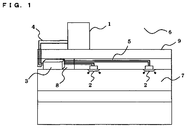
FIG. 1 illustrates an exemplary schematic of an embodiment of a chemical separation of the substrate part from the electrochemically active cell part of the electrochemical apparatus via a barrier layer, which includes a multitude of barrier sublayers.
FIG. 2 illustrates a schematic of an exemplary use of an embodiment of a barrier layer that includes barrier sublayers of different area dimensions and provides the electrical separation between the positive and negative part of the electrochemically active cell.
FIG. 3 a illustrates a schematic of an exemplary use of an embodiment of a barrier layer that includes an electrically conductive barrier sublayer for the case in which the electrical separation between the positive and the negative part of the electrochemically active cell is accomplished through fabrication of the negative part entirely on top of the electrolyte.
FIG. 3 b illustrates a schematic of another exemplary use of an embodiment of a barrier layer that includes an electrically conductive barrier sublayer on metallic substrate for the case in which the electrical separation between the positive and the negative part of the battery is accomplished through fabrication of the negative part entirely on top of the electrolyte.
FIG. 3 c illustrates a schematic of an exemplary use of an embodiment of a barrier layer that includes an electrically conductive barrier sublayer on metallic substrate for the case in which the electrical separation between the positive and the negative part of the battery is accomplished through fabrication of the positive part entirely on top of the electrolyte.
FIG. 4 a illustrates a schematic of an exemplary use of an embodiment of a barrier layer that includes electrically conductive barrier sublayers for the case in which the electrical separation between the positive and the negative part of the electrochemical active cell is not done via fabrication of the negative part entirely on top of the electrolyte.
FIG. 4 b illustrates a schematic of another exemplary use of an embodiment of a barrier layer that includes electrically conductive barrier sublayers for the case in which the electrical separation between the positive and the negative part of the electrochemically active cell is not done via fabrication of the negative part entirely on top of the electrolyte.
FIG. 4 c illustrates a schematic of another exemplary use of an embodiment of a barrier layer that includes electrically conductive barrier sublayers for the case in which the electrical separation between the positive and the negative part of the electrochemically active cell is not done via fabrication of the negative part entirely on top of the electrolyte while the negative anode has direct contact to a barrier sublayer.
FIG. 5 illustrates a graph of an X-ray diffraction (XRD) pattern of an embodiment of a 1.6 μm thick LiCoO.sub.2 positive cathode film fabricated onto 3000 Å Au cathode current collector over 300 Å Co adhesion layer attached to an electrically insulating barrier layer composed of two barrier sublayers, 5000 Å Al.sub.2O.sub.3 and 6000 Å CO.sub.3O.sub.4, on 50 μm thick stainless steel foil type 430 substrate.
FIG. 6 illustrates a graph of an X-ray diffraction (XRD) pattern of an embodiment of a 1.6 μm thick LiCoO.sub.2 positive cathode film fabricated onto 3000 Å Au cathode current collector over 300 Å Co adhesion layer over a barrier layer composed of two sublayers, 5000 Å Si.sub.3N.sub.4 and 5000 Å SiO.sub.2, on 300 μm thick silicon substrate.
FIG. 7 a illustrates a schematic of an embodiment of an anode configuration of the “normal configuration” in which the negative anode is not in direct contact with the barrier layer.
FIG. 7 b illustrates a schematic of an embodiment of an anode configuration of the “normal configuration” in which the negative anode is in direct contact with at least one of the barrier sublayers.
FIG. 8 illustrates a schematic of an embodiment of an anode configuration of the “normal configuration” in which the negative anode is in direct contact with an electrically conductive ZrN barrier sublayer that also serves as the anode current collector.
FIG. 9 illustrates a schematic of an embodiment of a battery configuration in which the negative anode is in direct contact with the substrate, in case the substrate is chemically inert to the negative anode. In this embodiment, the substrate can serve as the negative anode current collector and the negative terminal, if the substrate is sufficiently electrically conductive, as is the case for stainless steel, for example.
FIG. 10 illustrates a schematic of an embodiment of the use of a moisture protection layer to protect the moisture-sensitive electrolyte layer against moisture present in the ambient environment for the case in which the protective encapsulation has been fabricated with an opening for providing access to the negative terminal.
Detailed description of the invention
It should be understood that this invention is not limited to the particular methodology, protocols, etc., described herein and, as such, may vary. The terminology used herein is for the purpose of describing particular embodiments only, and is not intended to limit the scope of the present invention, which is defined solely by the claims.
As used herein and in the claims, the singular forms “a,” “an,” and “the” include the plural reference unless the context clearly indicates otherwise.
All patents and other publications identified are incorporated herein by reference in their entirety for the purpose of describing and disclosing, for example, the methodologies, apparatuses, and compositions described in such publications that might be used in connection with the present invention. These publications are provided solely for their disclosure prior to the filing date of the present application. Nothing in this regard should be construed as an admission that the inventors are not entitled to antedate such disclosure by virtue of prior invention or for any other reason.
Unless defined otherwise, all technical terms used herein have the same meaning as those commonly understood to one of ordinary skill in the art to which this invention pertains. Although any known methods, devices, and materials may be used in the practice or testing of the invention, certain exemplary preferred methods, devices, and materials in this regard are described here.
Thin-film batteries may, for example, be fabricated in batch mode by depositing the individual battery component layers sequentially. Once a substrate material has been selected, it may be prepared by cleaning and, if desired, other pre-treatments. The barrier layer composed of its barrier sublayers, which may be 0.5-5 μm thick in total, is the key to successful fabrication of thin-film batteries on metallic and polymeric foils as well as silicon. The barrier layer should be able to withstand the annealing temperatures for the positive cathode film together with the cathode current collector, remain chemically inert, and not be a source of impurities.
The description continues in the full USPTO document.
 Lapsed, fee not paid11 drawings