Background of the invention
1. Field of the invention
One embodiment of the present invention relates to a display device and a driving method of the display device.
In this specification, a semiconductor device means all types of devices which can function by utilizing semiconductor characteristics, and a semiconductor circuit, a memory device, an imaging device, a display device, an electro-optical device, an electronic device, and the like are all semiconductor devices.
2. Description of the related art
In recent years, display devices which can show pseudo stereoscopic images (three-dimensional images), such as a display device using a liquid crystal display device and a display device using an electroluminescent display device (also referred to as an EL display device), have been developed.
Examples of the display device which can show pseudo three-dimensional images include a display device making a viewer perceive two-dimensional images as three-dimensional images by utilizing parallax between the left eye and the right eye. In such a display device, for example, an image for the left eye (hereinafter referred to as a left-eye image) and an image for the right eye (hereinafter referred to as a right-eye image) are alternately displayed on a pixel portion, and a viewer sees the images with use of eyeglasses provided with shutters corresponding to both eyes. When a left-eye is displayed as a display image, the shutter for the right eye of the eyeglasses is closed, and light incident on the right eye of the viewer is blocked. When a right-eye image is displayed as a display image, the shutter for the left eye of the eyeglasses is closed, and light incident on the left eye of the viewer is blocked. As a result, two-dimensional images can be seen as pseudo three-dimensional images.
In addition, the following method (for example, Patent Document 1) is known. In each time of displaying a left-eye image and displaying a right-eye image, a unit frame period for displaying the image is divided into a plurality of subframe periods. A color of light emitted from a light unit (including a backlight) to a pixel circuit (also referred to as a display circuit) is changed every subframe period, whereby a full-color image is displayed every unit frame period (this method is called a field sequential method). When a field sequential method is employed, for example, a color filter is not needed in the liquid crystal display device, and thus, light transmittance can be increased.
In addition, a method in which the left-eye images and the right-eye images are each displayed continuously over a plurality of frame periods is known (for example, Patent Document 2). By the above method, an interval between operation of switching between a shutter for the left eye and a shutter for the right eye of the eyeglasses can be prolonged; thus, crosstalk can be suppressed even in the case of increasing the frame frequency. REFERENCE Patent Document
[Patent Document 1] Japanese Published Patent Application No. 2003-259395 [Patent Document 2] Japanese Published Patent Application No. 2009-031523 SUMMARY OF THE INVENTION
In a field-sequential liquid crystal display device, it is necessary to increase the frequency of input of an image signal to each pixel. For example, in the case where three-dimensional images are not displayed, in a field-sequential liquid crystal display device which includes light sources (a backlight) of three colors, red (R), green (G), and blue (B), the frequency of input of image signals to each pixel needs to be at least three times as high as that in a color-filter liquid crystal display device which includes a light source (a backlight) of white light. Specifically, in the case where the frame frequency is 60 Hz, it is necessary to input image signals to each pixel 60 times per second in a color-filter liquid crystal display device; on the other hand, it is necessary to input image signals to each pixel 180 times per second in a field-sequential liquid crystal display device which includes light sources (a backlignt) of three colors, red (R), green (G), and blue (B).
In the case where a field-sequential liquid crystal display device displays three-dimensional images, a period for displaying black (K) is needed in addition to periods for displaying the above three colors in order to switch the left-eye image and the right-eye image. Therefore, in the case where the field-sequential liquid crystal display device displays three-dimensional images, it is necessary to input image signals to each pixel 480 times per second.
As described above, in the field-sequential liquid crystal display device, color information is time-divided. For that reason, display perceived by a user is sometimes changed from display based on original display data because of a lack of given display data due to temporary interruption of display, such as a blink of the user (such a phenomenon is also referred to as color break or color breakup); thus, the display image quality is decreased.
An object of one embodiment of the present invention is to provide a display device with high display quality by suppressing decrease in image quality.
An object of one embodiment of the present invention is to provide a display device with low power consumption.
An object of one embodiment of the present invention is to provide a display device that can perform favorable stereoscopic display without decreasing resolution.
With use of a backlight including a plurality of backlight units each supplying light of different hues, writing of an image signal and lighting of the backlight are performed in individual regions or in individual backlight units in a pixel portion. Accordingly, a period during which a backlight is turned off can be shorter than that in a conventional method in which an image signal is written into the whole pixel portion and then a backlight is lit; therefore, a display device with high brightness and high display quality can be achieved.
One embodiment of the present invention is a driving method of a display device, in which a pixel portion including a plurality of pixels arranged in matrix is divided into plural regions, lighting of backlight units each emitting light of different hues is controlled in each region, and the backlight units of the plural regions are turned off simultaneously at a regular interval so as to display black.
The right-eye image and the left-eye image are alternately displayed with black display interposed therebetween, and light incident on the right eye of a viewer is blocked when a left-eye image is displayed, and light incident on the left eye of the viewer is blocked when a right-eye image is displayed. In addition, an image signal is written into a pixel in a black display period during which the backlight units are turned off, whereby display quality can be increased.
One embodiment of the present invention is a driving method of a liquid crystal display device including a pixel portion including a first region, a second region adjacent to the first region, and a third region adjacent to the second region; a plurality of pixels arranged in matrix in the first region, the second region, and the third region; and a plurality of backlight units overlapping with the plurality of pixels, in which a first subframe period, a second subframe period, a third subframe period, a fourth subframe period, a first hue display period, a second hue display period, a third hue display period, and a black display period are provided. In the driving method of a liquid crystal display device, during the first subframe period, the first hue is displayed in the first region, the third hue is displayed in the second region, and the second hue is displayed in the third region; during the second subframe period, the second hue is displayed in the first region, the first hue is displayed in the second region, and the third hue is displayed in the third region; during the third subframe period, the third hue is displayed in the first region, the second hue is displayed in the second region, and the first hue is displayed in the third region; and during the fourth subframe period, black is displayed in the first to third regions.
Another embodiment of the present invention is a driving method of a display device including: a pixel portion including a first region, a second region adjacent to the first region, and a third region adjacent to the second region; a plurality of pixels arranged in matrix in the first region, the second region, and the third region; and a plurality of backlight units for supplying light of a first hue, light of a second hue, and light of a third hue, the plurality of backlight units overlapping with the plurality of pixels, wherein a right-eye image display period for displaying a right-eye image and a left-eye image display period for displaying a left-eye image are provided, wherein the right-eye image display period and the left-eye image display period each comprise a first subframe period, a second subframe period, a third subframe period, and a fourth subframe period, wherein during the first subframe period, a first hue signal is supplied to the plurality of pixels included in the first region, and then the backlight unit supplies the light of the first hue; a third hue signal is supplied to the plurality of pixels included in the second region, and then the backlight unit supplies the light of the third hue; and a second hue signal is supplied to the plurality of pixels included in the third region, and then the backlight unit supplies the light of the second hue, wherein during the second subframe period, the second hue signal is supplied to the plurality of pixels included in the first region, and then the backlight unit supplies the light of the second hue; the first hue signal is supplied to the plurality of pixels included in the second region, and then the backlight unit supplies the light of the first hue; and the third hue signal is supplied to the plurality of pixels included in the third region, and then the backlight unit supplies the light of the third hue, wherein during the third subframe period, the third hue signal is supplied to the plurality of pixels included in the first region, and then the backlight unit supplies the light of the third hue; the second hue signal is supplied to the plurality of pixels included in the second region, and then the backlight unit supplies the light of the second hue; and the first hue signal is supplied to the plurality of pixels included in the third region, and then the backlight unit supplies the light of the first hue, wherein during the fourth subframe period, the plurality of backlight units in the first region, the second region, and the third region is turned off, and wherein the right-eye image and the left-eye image are displayed alternately.
In the first subframe period, a hue signal which is the same as a hue signal held in the fourth subframe period is held in a pixel included in the first region and adjacent to the second region.
In the first subframe period, a hue signal which is the same as a hue signal held in the fourth subframe period is held in a pixel included in the second region and adjacent to the third region.
In the fourth subframe period, a hue signal which is the same as a hue signal held in the first subframe period is held in a pixel included in the second region and adjacent to the first region.
In the fourth subframe period, a hue signal which is the same as a hue signal held in the first subframe period is held in a pixel included in the third region and adjacent to the second region.
The right-eye image and the left-eye image are displayed alternately, whereby three-dimensional images can be preceived by a viewer.
A display device with high display quality can be provided.
A display device with low power consumption can be provided.
A display device that can perform favorable stereoscopic display can be provided without decreasing resolution.
Brief description of the drawings
In the accompanying drawings:
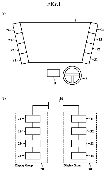
FIGS. 1A and 1B illustrate a structure example of a liquid crystal display device;
FIGS. 2A and 2C illustrate a configuration example and FIG. 2B illustrates an operation example of a scan line driver circuit;
FIG. 3A illustrates a configuration example and FIGS. 3B to 3D illustrate operation examples of pulse output circuits;
FIG. 4 illustrates an operation example of a scan line driver circuit;
FIG. 5A illustrates a configuration example of a signal line driver circuit and
FIG. 5B illustrates an example of a timing for supplying an image signal;
FIGS. 6A and 6B illustrate structure examples of a backlight;
FIG. 7 illustrates an operation example of a liquid crystal display device;
FIG. 8 illustrates an operation example of a liquid crystal display device;
FIG. 9 illustrates an operation example of a liquid crystal display device;
FIGS. 10A and 10B illustrate an operation example of a liquid crystal display device;
FIGS. 11A to 11G illustrate an operation example of a liquid crystal display device;
FIGS. 12A to 12D illustrate structure examples of a transistor in cross section;
FIGS. 13A and 13B illustrate an example of a panel of a liquid crystal display device;
FIG. 14 illustrates a structure example of a liquid crystal display device; and
FIGS. 15A to 15D illustrate structure examples of electronic devices.
Detailed description of the invention
Hereinafter, embodiments of the present invention will be described with reference to the accompanying drawings. Note that the present invention can be carried out in many different modes, and it is easily understood by those skilled in the art that modes and details of the present invention can be modified in various ways without departing from the spirit and scope of the present invention. Therefore, the present invention is not interpreted as being limited to the description of the embodiments below. Note that in structures of the present invention described below, reference numerals denoting the same portions are used in common in different drawings.
Note that the size, the thickness of a layer, a signal waveform, and a region of each structure illustrated in the drawings and the like in the embodiments are exaggerated for simplicity in some cases. Therefore, the embodiments of the present invention are not limited to such scales.
Note that terms such as first, second, third to N-th (N is a natural number) employed in this specification are used in order to avoid confusion between components and do not set a limitation on number. The natural number is 1 or more unless otherwise specified.
A transistor is a kind of semiconductor elements and can achieve amplification of current or voltage, switching operation for controlling conduction or non-conduction, or the like. A transistor in this specification includes an insulated-gate field effect transistor (IGFET) and a thin film transistor (TFT).
Functions of a “source” and a “drain” of a transistor might interchange when a transistor of opposite polarity is used or the direction of current flow is changed in circuit operation, for example. Therefore, the terms “source” and “drain” can be replaced with each other in this specification. Embodiment 1
In this embodiment, a liquid crystal display device which is one embodiment of the present invention is described with reference to FIGS. 1A and 1B , FIGS. 2A to 2C , FIGS. 3A to 3D , FIG. 4 , FIGS. 5A and 5B , FIGS. 6A and 6B , FIG. 7 , FIG. 8 , FIG. 9 , FIGS. 10A and 10B , and FIGS. 11A to 11G .
<Structure Example of Liquid Crystal Display Device>
FIG. 1A illustrates a structure example of a liquid crystal display device 100 . The liquid crystal display device 100 illustrated in FIG. 1A includes a pixel portion 10 , a scan line driver circuit 11 , a signal line driver circuit 12 , m scan lines 13 arranged in parallel or in substantially parallel, whose potentials are controlled by the scan line driver circuit 11 , and n signal lines 14 arranged in parallel or in substantially parallel, whose potentials are controlled by the signal line driver circuit 12 . The pixel portion 10 is divided into three regions (regions 101 to 103 ), and each region includes a plurality of pixels 15 arranged in matrix.
The scan lines 13 are electrically connected to respective n pixels in respective rows, among the plurality of pixels arranged in m rows by n columns in the pixel portion 10 (m is a natural number larger than or equal to 12, and n is a natural number). In addition, the signal lines 14 are electrically connected to respective m pixels in respective columns, among the plurality of pixels arranged in m rows by n columns.
The m scan lines 13 are divided into a plurality of groups in accordance with the number of regions included in the pixel portion 10 . For example, the m scan lines 13 are divided into three groups because the pixel portion 10 is divided into three regions in FIG. 1A . The scan lines 13 in each group are electrically connected to the plurality of pixels 15 in a region corresponding to the group. Specifically, in each of the regions, each of the scan lines 13 is electrically connected to n pixels 15 in a corresponding row, among the plurality of pixels 15 arranged in matrix.
Regardless of the above regions, the n signal lines 14 are electrically connected to respective m pixels 15 in respective columns, among the plurality of pixels 15 arranged in m rows by n columns in the pixel portion 10 .
FIG. 1B illustrates an example of a circuit configuration of a pixel 15 included in the pixel portion 10 illustrated in FIG. 1A . The pixel 15 illustrated in FIG. 1B includes a transistor 16 , a capacitor 17 , and a liquid crystal element 18 .
A gate of the transistor 16 is electrically connected to the scan line 13 and one of a source and a drain thereof is electrically connected to the signal line 14 . One electrode of the capacitor 17 is electrically connected to the other of the source and the drain of the transistor 16 . The other electrode of the capacitor 17 is electrically connected to a wiring for supplying a capacitor potential (the wiring is also referred to as a capacitor wiring). One of electrodes (also referred to as a pixel electrode) of the liquid crystal element 18 is electrically connected to the other of the source and the drain of the transistor 16 and the one electrode of the capacitor 17 , and the other electrode (also referred to as a counter electrode) of the liquid crystal element 18 is electrically connected to a wiring for supplying a counter potential.
Note that although the transistor 16 is an n-channel transistor in this embodiment, the transistor 16 may be a p-channel transistor. The capacitor potential and the counter potential can be equal to each other.
<Configuration Example of Scan Line Driver Circuit>
FIG. 2A illustrates a configuration example of the scan line driver circuit 11 included in the liquid crystal display device 100 illustrated in FIG. 1A . The scan line driver circuit 11 illustrated in FIG. 2A includes: wirings for supplying respective first to fourth scan line driver circuit clock signals (GCK 1 to GCK 4 ); wirings for supplying respective first to sixth pulse-width control signals (PWC 1 to PWC 6 ); and a first pulse output circuit 20 _ 1 which is electrically connected to the scan line 13 in the first row to an m-th pulse output circuit 20 _ m which is electrically connected to the scan line 13 in the m-th row.
In this embodiment, the first pulse output circuit 20 _ 1 to the k-th pulse output circuit 20 _ k (k is a natural number less than or equal to m/3) are electrically connected to scan lines 13 _ 1 to 13 _ k provided in the region 101 , respectively. In this embodiment, k is preferably a multiple of the number of clock signals (GCK 1 to GCK 4 ) supplied to the scan line driver circuit 11 , i.e., a multiple of 4.
In addition, the (k+1)th to 2k-th pulse output circuits 20 _ k+ 1 to 20 _2k are electrically connected to the scan lines 13 _ k+ 1 to 13 _2k provided in the region 102 . Further, the (2k+1)th to m-th pulse output circuits 20 _2k+1 to 20 _ m are electrically connected to the scan lines 13 _2k+1 to 13 _ m provided in the region 103 .
The first to m-th pulse output circuits 20 _ 1 to 20 _ m have a function of sequentially shifting a shift pulse in each shift period in response to a scan line driver circuit start pulse GSP which is input to the first pulse output circuit 20 _ 1 . Further, a plurality of shift pulses can be shifted in the first to m-th pulse output circuits 20 _ 1 to 20 _ m concurrently. In other words, even in a period during which a shift pulse is shifted in the first to m-th pulse output circuits 20 _ 1 to 20 _ m , the scan line driver circuit start pulse GSP can be input to the first pulse output circuit 20 _ 1 .
FIG. 2B illustrates examples of specific operation of the above signals. The first scan line driver circuit clock signal (GCK 1 ) in FIG. 2B periodically repeats a high-level potential (high power supply potential (V.sub.dd)) and a low-level potential (low power supply potential (V.sub.ss)) and has a duty ratio of 1/4. The phase of the second scan line driver circuit clock signal (GCK 2 ) is shifted from the first scan line driver circuit clock signal (GCK 1 ) by ¼ period. The phase of the third scan line driver circuit clock signal (GCK 3 ) is shifted from the first scan line driver circuit clock signal (GCK 1 ) by ½ period. The phase of the fourth scan line driver circuit clock signal (GCK 4 ) is shifted from the first scan line driver circuit clock signal (GCK 1 ) by ¾ period.
The first pulse width control signal (PWC 1 ) in FIG. 2B periodically repeats the high-level potential (high power supply potential (V.sub.dd)) and the low-level potential (low power supply potential (V.sub.ss)) and has a duty ratio of 1/3. The phase of the second pulse width control signal (PWC 2 ) is shifted from the first pulse width control signal (PWC 1 ) by ⅙ period. The phase of the third pulse width control signal (PWC 3 ) is shifted from the first pulse width control signal (PWC 1 ) by ⅓ period. The phase of the fourth pulse width control signal (PWC 4 ) is shifted from the first pulse width control signal (PWC 1 ) by ½ period. The phase of the fifth pulse width control signal (PWC 5 ) is shifted from the first pulse width control signal (PWC 1 ) by ⅔ period. The phase of the sixth pulse width control signal (PWC 6 ) is shifted from the first pulse width control signal (PWC 1 ) by ⅚ period.
Note that here, the ratio of the pulse width of each of the first to fourth scan line driver circuit clock signals (GCK 1 to GCK 4 ) to the pulse width of each of the first to sixth pulse width control signals (PWC 1 to PWC 6 ) is 3:2.
In the liquid crystal display device 100 , circuits with the same configuration can be used as the first to m-th pulse output circuits 20 _ 1 to 20 _ m . Note that electrical connection relations of a plurality of terminals included in the pulse output circuit differ depending on the pulse output circuits. Specific connection relations are described with reference to FIGS. 2A and 2C .
Each of the first to m-th pulse output circuits 20 _ 1 to 20 _ m has terminals 21 to 27 . The terminals 21 to 24 and the terminal 26 are input terminals. The terminals 25 and 27 are output terminals.
First, the terminal 21 is described. The terminal 21 in the first pulse output circuit 20 _ 1 is electrically connected to a wiring that supplies the scan line driver circuit start signal (GSP). The terminal 21 in each of the second to m-th pulse output circuits 202 to 20 _ m is electrically connected to the terminal 27 in the pulse output circuit in the preceding stage.
Next, the terminal 22 is described. The terminal 22 in the (4a−3)th pulse output circuit (a is a natural number less than or equal to m/4) is electrically connected to the wiring that supplies the first scan line driver circuit clock signal (GCK 1 ). The terminal 22 in the (4a−2)th pulse output circuit is electrically connected to the wiring that supplies the second scan line driver circuit clock signal (GCK 2 ). The terminal 22 in the (4a−1)th pulse output circuit is electrically connected to the wiring that supplies the third scan line driver circuit clock signal (GCK 3 ). The terminal 22 in the 4a-th pulse output circuit is electrically connected to the wiring that supplies the fourth scan line driver circuit clock signal (GCK 4 ).
Then, the terminal 23 is described. The terminal 23 in the (4a−3)th pulse output circuit is electrically connected to the wiring that supplies the second scan line driver circuit clock signal (GCK 2 ). The terminal 23 in the (4a−2)th pulse output circuit is electrically connected to the wiring that supplies the third scan line driver circuit clock signal (GCK 3 ). The terminal 23 in the (4a−1)th pulse output circuit is electrically connected to the wiring that supplies the fourth scan line driver circuit clock signal (GCK 4 ). The terminal 23 in the 4a-th pulse output circuit is electrically connected to the wiring that supplies the first scan line driver circuit clock signal (GCK 1 ).
Next, the terminal 24 is described. The terminal 24 in the (2b−1)th pulse output circuit (b is a natural number less than or equal to k/2) is electrically connected to the wiring that supplies the first pulse width control signal (PWC 1 ). The terminal 24 in the 2b-th pulse output circuit is electrically connected to the wiring that supplies the fourth pulse width control signal (PWC 4 ). The terminal 24 in the (2c−1)th pulse output circuit (c is a natural number greater than or equal to (k/2+1) and less than or equal to k) is electrically connected to the wiring that supplies the second pulse width control signal (PWC 2 ). The terminal 24 in the 2c-th pulse output circuit is electrically connected to the wiring that supplies the fifth pulse width control signal (PWC 5 ). The terminal 24 in the (2d−1)th pulse output circuit (d is a natural number greater than or equal to (k+1) and less than or equal to m/2) is electrically connected to the wiring that supplies the third pulse width control signal (PWC 3 ). The terminal 24 in the 2d-th pulse output circuit is electrically connected to the wiring that supplies the sixth pulse width control signal (PWC 6 ).
Then, the terminal 25 is described. The terminal 25 in the x-th pulse output circuit (x is a natural number less than or equal to m) is electrically connected to the scan line 13 _ x in the x-th row.
Next, the terminal 26 is described. The terminal 26 in the y-th pulse output circuit (y is a natural number less than or equal to (m−1)) is electrically connected to the terminal 27 in the (y+1)th pulse output circuit. The terminal 26 in the m-th pulse output circuit is electrically connected to a wiring that supplies an m-th pulse output circuit stop signal (STP).
Note that if an (m+1)th pulse output circuit is provided, the m-th pulse output circuit stop signal (STP) corresponds to a signal output from the terminal 27 in the (m+1)th pulse output circuit. Specifically, the m-th pulse output circuit stop signal (STP) can be supplied to the m-th pulse output circuit by provision of the (m+1)th pulse output circuit as a dummy circuit or by direct input of the signal from the outside.
The connection relation of the terminal 27 in each of the pulse output circuits is described above. Thus, the above description is referred to here.
<Configuration Example of Pulse Output Circuit>
FIG. 3A illustrates a configuration example of the pulse output circuit illustrated in FIGS. 2A and 2C . The pulse output circuit illustrated in FIG. 3A includes transistors 31 to 39 .
One of a source and a drain of the transistor 31 is electrically connected to a wiring that supplies the high power supply potential (V.sub.dd) (hereinafter also referred to as a high power supply potential line). A gate of the transistor 31 is electrically connected to the terminal 21 .
One of a source and a drain of the transistor 32 is electrically connected to a wiring that supplies the low power supply potential (V.sub.ss) (hereinafter also referred to as a low power supply potential line). The other of the source and the drain of the transistor 32 is electrically connected to the other of the source and the drain of the transistor 31 .
One of a source and a drain of the transistor 33 is electrically connected to the terminal 22 . The other of the source and the drain of the transistor 33 is electrically connected to the terminal 27 . A gate of the transistor 33 is electrically connected to the other of the source and the drain of the transistor 31 and the other of the source and the drain of the transistor 32 .
One of a source and a drain of the transistor 34 is electrically connected to the low power supply potential line, the other of the source and the drain of the transistor 34 is electrically connected to the terminal 27 , and a gate of the transistor 34 is electrically connected to a gate of the transistor 32 .
One of a source and a drain of the transistor 35 is electrically connected to the low power supply potential line. The other of the source and the drain of the transistor 35 is electrically connected to a gate of the transistor 32 and a gate of the transistor 34 . A gate of the transistor 35 is electrically connected to the terminal 21 .
One of a source and a drain of the transistor 36 is electrically connected to the high power supply potential line. The other of the source and the drain of the transistor 36 is electrically connected to the gate of the transistor 32 , the gate of the transistor 34 , and the other of the source and the drain of the transistor 35 . A gate of the transistor 36 is electrically connected to the terminal 26 .
One of a source and a drain of the transistor 37 is electrically connected to the high power supply potential line. The other of the source and the drain of the transistor 37 is electrically connected to the gate of the transistor 32 , the gate of the transistor 34 , the other of the source and the drain of the transistor 35 , and the other of the source and the drain of the transistor 36 . A gate of the transistor 37 is electrically connected to the terminal 23 .
One of a source and a drain of the transistor 38 is electrically connected to the terminal 24 . The other of the source and the drain of the transistor 38 is electrically connected to the terminal 25 . A gate of the transistor 38 is electrically connected to the other of the source and the drain of the transistor 31 , the other of the source and the drain of the transistor 32 , and the gate of the transistor 33 .
One of a source and a drain of the transistor 39 is electrically connected to the low power supply potential line. The other of the source and the drain of the transistor 39 is electrically connected to the terminal 25 . A gate of the transistor 39 is electrically connected to the gate of the transistor 32 , the gate of the transistor 34 , the other of the source and the drain of the transistor 35 , the other of the source and the drain of the transistor 36 , and the other of the source and the drain of the transistor 37 .
Note that in the following description, a node to which the other of the source and the drain of the transistor 31 , the other of the source and the drain of the transistor 32 , the gate of the transistor 33 , and the gate of the transistor 38 are electrically connected is referred to as a node A. In addition, a node to which the gate of the transistor 32 , the gate of the transistor 34 , the other of the source and the drain of the transistor 35 , the other of the source and the drain of the transistor 36 , the other of the source and the drain of the transistor 37 , and the gate of the transistor 39 are electrically connected is referred to as a node B.
<Operation Example of Pulse Output Circuit>
An operation example of the pulse output circuit is described with reference to FIGS. 3B to 3D . Note that here, the following case is described: an operation example at the time when timing of inputting the scan line driver circuit start pulse (GSP) to the terminal 21 in the first pulse output circuit 20 _ 1 is controlled so that shift pulses are output from the terminals 27 in the first pulse output circuit 20 _ 1 , the (k+1)th pulse output circuit 20 _ k+ 1, and the (2k+1)th pulse output circuit 20 _2k+1 at the same timing.
As a specific example, FIG. 3B illustrates the potentials of signals input to the terminals in the first pulse output circuit 20 _ 1 and the potentials of the node A and the node B at the time when the scan line driver circuit start pulse (GSP) is input. FIG. 3C illustrates the potentials of signals input to the terminals in the (k+1)th pulse output circuit 20 _ k+ 1 and the potentials of the node A and the node B at the time when the high-level potential is input from the k-th pulse output circuit 20 _ k . FIG. 3D illustrates the potentials of signals input to the terminals in the (2k+1)th pulse output circuit 20 _2k+1 and the potentials of the node A and the node B at the time when the high-level potential is input from the 2k-th pulse output circuit 20 _2k.
Note that in FIGS. 3B to 3D , the signals input to the terminals are provided in parentheses. Further, FIGS. 3B to 3D illustrate signals (Gout 2 , Gout k+2, and Gout 2k+2) output from the terminals 25 in the pulse output circuits provided in subsequent stages (the second pulse output circuit 20 _ 2 , the (k+2)th pulse output circuit 20 _ k+ 2, and the (2k+2)th pulse output circuit 20 _2k+2), and output signals of the terminals 27 in the pulse output circuits provided in subsequent stages (SRout 2 : an input signal of the terminal 26 in the first pulse output circuit 20 _ 1 , SRout k+2: an input signal of the terminal 26 in the (k+1)th pulse output circuit 20 _ k+ 1, and SRout 2k+2: an input signal of the terminal 26 in the (2k+1)th pulse output circuit 20 _2k+1). Note that in FIGS. 3B to 3D , Gout represents an output signal from the pulse output circuit to the scan line, and SRout represents an output signal from the pulse output circuit to the pulse output circuit in the subsequent stage.
First, the case where the high-level potential is input to the first pulse output circuit 20 _ 1 as the scan line driver circuit start pulse (GSP) is described with reference to FIG. 3B .
In a period t 1 , the high-level potential (high power supply potential (V.sub.dd)) is input to the terminal 21 . Thus, the transistors 31 and 35 are turned on. As a result, the potential of the node A is increased to a high-level potential (a potential decreased from the high power supply potential (V.sub.dd) by the threshold voltage of the transistor 31 ), and the potential of the node B is decreased to the low power supply potential (V.sub.ss). Consequently, the transistors 33 and 38 are turned on and the transistors 32 , 34 , and 39 are turned off.
Thus, in the period t 1 , a signal output from the terminal 27 is a signal input to the terminal 22 , and a signal output from the terminal 25 is a signal input to the terminal 24 . Here, in the period t 1 , both the signal input to the terminal 22 and the signal input to the terminal 24 have the low-level potentials (low power supply potentials (V.sub.ss)). Accordingly, in the period t 1 , the first pulse output circuit 20 _ 1 outputs the low-level potential (low power supply potential (V.sub.ss)) to the terminal 21 in the second pulse output circuit 20 _ 2 and the scan line provided in the first row in the pixel portion.
In a period t 2 , signals input to the terminals are not changed from those in the period t 1 . Thus, the signals output from the terminals 25 and 27 are not changed, and the low-level potentials (low power supply potentials (V.sub.ss)) are output from the terminals 25 and 27 .
In a period t 3 , the high-level potential (high power supply potential (V.sub.dd)) is input to the terminal 24 . Note that the potential of the node A (the potential of the source of the transistor 31 ) is increased to the high-level potential (a potential decreased from the high power supply potential (V.sub.dd) by the threshold voltage of the transistor 31 ) in the period t 1 . Thus, the transistor 31 is off. At this time, the high-level potential (high power supply potential (V.sub.dd)) is input to the terminal 24 , so that the potential of the node A (the potential of the gate of the transistor 38 ) is further increased by capacitive coupling of the source and the gate of the transistor 38 (bootstrap operation). Since the potential of the node A is increased by the bootstrap operation, the potential of the signal output from the terminal 25 is not decreased from the high-level potential (high power supply potential (V.sub.dd)) input to the terminal 24 . Accordingly, in the period t 3 , the first pulse output circuit 20 _ 1 outputs the high-level potential (the high power supply potential (V.sub.dd)=a selection signal) to the scan line provided in the first row in the pixel portion.
In a period t 4 , the high-level potential (high power supply potential (V.sub.dd)) is input to the terminal 22 . Here, since the potential of the node A is increased by the bootstrap operation, the potential of the signal output from the terminal 27 is not decreased from the high-level potential (high power supply potential (V.sub.dd)) input to the terminal 22 . Accordingly, in the period t 4 , the terminal 27 outputs the high-level potential (high power supply potential (V.sub.dd)) which is input to the terminal 22 . In other words, the first pulse output circuit 20 _ 1 outputs the high-level potential (the high power supply potential (V.sub.dd)=the shift pulse) to the terminal 21 in the second pulse output circuit 20 _ 2 . In the period t 4 , a signal input to the terminal 24 is kept at the high-level potential (high power supply potential (V.sub.dd)); thus, the signal which is output from the first pulse output circuit 20 _ 1 to the scan line provided in the first row in the pixel portion is kept at the high-level potential (the high power supply potential (V.sub.dd)=the selection signal). Note that the transistor 35 is turned off because the low-level potential (low power supply potential (V.sub.ss)) is input to the terminal 21 , which does not directly influence output signals of the pulse output circuit in the period t 4 .
In a period t 5 , the low-level potential (low power supply potential (V.sub.ss)) is input to the terminal 24 . Here, the transistor 38 is kept on. Accordingly, in the period t 5 , a signal output from the first pulse output circuit 20 _ 1 to the scan line provided in the first row in the pixel portion has the low-level potential (low power supply potential (V.sub.ss)).
In a period t 6 , signals input to the terminals are not changed from those in the period t 5 . Thus, the signals output from the terminals 25 and 27 are not changed, the low-level potential (low power supply potential (V.sub.ss)) is output from the terminal 25 , and the high-level potential (high power supply potential (V.sub.dd)=the shift pulse) is output from the terminal 27 .
The description continues in the full USPTO document.
 Lapsed, fee not paid4 drawings