Background
Image data captured by an image sensor is often initially processed as part of an image processing pipeline in order to prepare the captured image data for further processing or consumption. In this way, real-time corrections or enhancements can be made without consuming other system resources. For example, raw image data may be corrected, filtered, or otherwise modified to provide subsequent components, such as a video encoder, with appropriately scaled image data for encoding and subsequent display, reducing a number of subsequent operations to be performed on the image data at the video encoder.
In order to implement these corrections or enhancements for captured image data, various different devices, components, units, or other modules may be used to implement the varying operations performed as part of an image processing pipeline. An image signal processor, for instance, may include multiple different units or stages at which different image modifications or enhancements can be made to image data obtained from an image sensor. Given the ubiquity of image sensors in many different products, efficiently handling image data as part of an image processing pipeline may confer relief on those products with constrained resources for performing additional tasks.
Summary
An image signal processor (ISP) of a device, apparatus, or computing system that includes a camera or other image sensor capable of capturing image data may include an image signal processor (ISP) pipeline that may implement one or more stages that process image data obtained from an image sensor of a camera via a sensor interface of the ISP. The sensor interface may perform various preprocessing operations on the raw image data, such as pixel bit shift and replication to convert the smaller bit width raw pixel data to 16-bit raw pixel data, pixel defect preprocessing for the raw pixel data to adjust values of patterned defect pixels created at the image sensor by special pixels such as focus pixels used to detect phase difference for auto focus, image cropping to reduce image data size, pixel binning, and/or horizontal pixel scaling. Patterned defect pixels are partially blocked or shielded at the image sensor, and thus less light is collected at these pixels during exposure. Thus, the patterned defect pixels tend to be darker than their normal neighbor pixels.
The sensor interface may include a pixel defect preprocessing stage or component that performs an initial adjustment of the pixel values for the patterned defect pixels. In some embodiments, to perform the preprocessing of the patterned defect pixels, the pixel defect preprocessing component may apply gain to the value of each of the pixels in the pattern. Neighbor normal pixels are not affected. To apply gain to a particular pixel, the pixel defect preprocessing component may determine a gain value for the pixel from a two-dimensional (2D) gain lookup table, e.g. a 17×17 table, for image(s) captured by the image sensor. The pixel defect preprocessing component may apply an interpolation technique (e.g., bilinear interpolation) to values in the table to determine a gain value for the pixel's location. The gain value may then be applied to the pixel value. The values in the gain lookup table may, for example, be determined during a calibration process for the image sensor. Alternatively, the values in the gain lookup table may be dynamically determined for the current image or for one or more previously captured image.
The pixel defect preprocessing component may output the preprocessed pixels in the image with the values of the patterned defect pixels adjusted by the gain values to the ISP pipeline for additional processing, and may also output the preprocessed pixels to memory (e.g., via direct memory access (DMA) technology), and/or to one or more other components or processes. The other components or processes may, for example, include an autofocus process, an image statistics block that generates statistics for auto exposure, white balance, or other processes, and a process that detects key points in images (e.g., for use in facial recognition, computer vision, and/or image matching processes).
In some embodiments, the ISP may include a pixel defect correction stage or component that may receive the original pixels and/or the output pixels from the pixel defect preprocessing component and perform a more rigorous correction of the patterned defect pixels as well as other defective pixels in the image, for example using a weighted combination of neighboring pixels. Thus, output of the pixel defect correction component may be of higher visual quality than the output of the pixel defect preprocessing component. However, in some embodiments, the pixel defect preprocessing component may be simpler, faster, and may take up less real estate in the ISP than the pixel defect correction component. Thus, the pixel defect preprocessing component may output the image data with the adjusted patterned defect pixel values for use by other processes or components such as auto focus or an image statistics block that may not require the image quality provided by the pixel defect correction component. Further, the pixel defect preprocessing component may allow the other processes or components to process image pixel data more quickly substantially in parallel with the ISP pipeline processing, since the other processes or components do not have to wait for the output of the pixel defect correction component to process the pixel data.
Brief description of the drawings
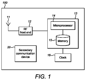
FIG. 1 is a logical block diagram illustrating an example system that may implement an image processing pipeline that processes image data at multiple rates, according to some embodiments.
FIG. 2 is a logical block diagram illustrating example data paths in a system that may implement an image processing pipeline that processes image data at multiple rates, according to some embodiments.
FIG. 3 is a logical block diagram illustrating an example image signal processor, according to some embodiments.
FIG. 4 is a logical block diagram illustrating operations of a sensor interface component in an image signal processor, according to some embodiments.
FIG. 5 provides an example of patterned defect pixels in an image frame captured by an image sensor, according to some embodiments.
FIG. 6 is a logical block diagram illustrating components and operations of a sensor interface component in more detail, according to some embodiments.
FIG. 7 is a high-level flowchart illustrating various methods and techniques for preprocessing image data in an image signal processor, according to some embodiments.
This specification includes references to “one embodiment” or “an embodiment.” The appearances of the phrases “in one embodiment” or “in an embodiment” do not necessarily refer to the same embodiment. Particular features, structures, or characteristics may be combined in any suitable manner consistent with this disclosure.
“Comprising.” This term is open-ended. As used in the appended claims, this term does not foreclose additional structure or steps. Consider a claim that recites: “An apparatus comprising one or more processor units . . . .” Such a claim does not foreclose the apparatus from including additional components (e.g., a network interface unit, graphics circuitry, etc.).
“Configured To.” Various units, circuits, or other components may be described or claimed as “configured to” perform a task or tasks. In such contexts, “configured to” is used to connote structure by indicating that the units/circuits/components include structure (e.g., circuitry) that performs those task or tasks during operation. As such, the unit/circuit/component can be said to be configured to perform the task even when the specified unit/circuit/component is not currently operational (e.g., is not on). The units/circuits/components used with the “configured to” language include hardware—for example, circuits, memory storing program instructions executable to implement the operation, etc. Reciting that a unit/circuit/component is “configured to” perform one or more tasks is expressly intended not to invoke 35 U.S.C. §112, paragraph (f), for that unit/circuit/component. Additionally, “configured to” can include generic structure (e.g., generic circuitry) that is manipulated by software or firmware (e.g., an FPGA or a general-purpose processor executing software) to operate in manner that is capable of performing the task(s) at issue. “Configure to” may also include adapting a manufacturing process (e.g., a semiconductor fabrication facility) to fabricate devices (e.g., integrated circuits) that are adapted to implement or perform one or more tasks.
“First,” “Second,” etc. As used herein, these terms are used as labels for nouns that they precede, and do not imply any type of ordering (e.g., spatial, temporal, logical, etc.). For example, a buffer circuit may be described herein as performing write operations for “first” and “second” values. The terms “first” and “second” do not necessarily imply that the first value must be written before the second value.
“Based On” or “Dependent On.” As used herein, these terms are used to describe one or more factors that affect a determination. These terms do not foreclose additional factors that may affect a determination. That is, a determination may be solely based on those factors or based, at least in part, on those factors. Consider the phrase “determine A based on B.” While in this case, B is a factor that affects the determination of A, such a phrase does not foreclose the determination of A from also being based on C. In other instances, A may be determined based solely on B.
When used in the claims, the term “or” is used as an inclusive or and not as an exclusive or. For example, the phrase “at least one of x, y, or z” means any one of x, y, and z, as well as any combination thereof.
Detailed description
An image signal processor or other image processing pipeline may implement many different techniques or components to correct or enhance image data captured by an image sensor. However, image data captured by the image data is not always utilized for the same purposes. For example, an image sensor may provide a stream of image data in order to display a preview image of what may be captured by the image sensor in higher resolution still image or recorded in a video. Depending on the desired effects or formats according to which image data captured by the image sensor may be processed, different portions of an image processing pipeline that processes the image data may be over or under-utilized. For example, for image data captured by a high-resolution image sensor that is being recorded as part of a lower resolution video file, some portions of an image processing pipeline may be over utilized (e.g., those portions of the pipeline processing the full-resolution image data which may be ultimately discarded in order to scale the image for the low resolution video).
In various embodiments, the image signal processor may process image data in an image processing pipeline at multiple rates in order to more efficiently leverage the processing capabilities of the image processing pipeline. For instance, in at least some embodiments one or more front-end pipeline stages may process image data at an initial rate, such as 2 pixels per clock cycle (ppc). In this way large amounts of image data (e.g., either as large individual image frames or a high rate of image frames, such as may be captured when recording slow motion video) may receive initial processing to reduce or correct image signal noise, artifacts, and other image defects that may be introduced as a result of collecting and processing image data. The image data may then be downscaled to a desired size and processed at a different rate, such as 1 ppc, at one or more back-end pipeline stages to perform other operations on the image frames in order to reduce image signal noise, correct color and image defects, as well as apply various special effects, so that processing is not performed upon image data that may be discarded.
In at least some embodiments, image data captured and processed through front-end pipeline stages may be stored in raw or full-color formats to a memory, while a scaled version of the image data may continue to be processed through the back-end pipeline stages of the image processing pipeline. In this way, high-resolution versions of image frames with some image processing may be captured while simultaneously continuing processing for lower resolution versions of the image frames (e.g., capturing high resolution stills of image frames that are also recorded in a lower resolution video).
In at least some embodiments, a back-end interface may be implemented to allow image data collected from sources different than the image sensor to be processed through back-end pipeline stage(s) of the image processing pipeline. For instance, image data received at a device that implements the image processing pipeline (e.g., a mobile computing device) from a remote device (e.g., a content server of a content provider, such as a web-based video service) may be received via the back-end interface and processed through the back-end pipeline stage(s) in order to perform operations to reduce image signal noise, correct color and image defects, or apply various special effects. In this way, the dedicated image processing components of the image processing pipeline may be utilized to efficiently perform image processing for image data received from many other sources.
The techniques described herein for processing image data in an image processing pipeline at multiple rates may be further illustrated in terms of an example system that employs them. As noted above, these techniques may be implemented in any type of camera, apparatus, or computing system that includes the capability to capture and process image data, including video clips.
One example of a system that is configured to implement any or all of the techniques described herein is illustrated in FIG. 1 . For example, system 100 illustrated in FIG. 1 may be configured to perform image processing using an image signal processor without the additional system memory operations required by existing GPU and CPU approaches. In the illustrated embodiment, system 100 includes image sensor(s) 102 , a system-on-a chip (SOC) component 104 , system memory (e.g., DRAM) 130 , persistent storage (e.g., flash memory) 128 , and a display 116 (e.g., LCD or OLED). In this example, image sensor(s) 102 may be any type of image sensor suitable for capturing image data (e.g., an image sensor that is responsive to captured light), such as an active-pixel sensor (e.g., complementary metal-oxide-semiconductor (CMOS) active-pixel sensor) on a camera, video camera, or other device that includes a camera or video camera. In this example, display 116 may be configured to display a preview of captured still images or video clips (which may be provided as output from image signal processor 106 ). Display 116 may also be configured to display menus, selected operating parameters, or other information received from a user interface of the system (not shown). In other embodiments, other types of display devices may be included in the system for these purposes. In different embodiments, system 100 may be any of various types of devices, including, but not limited to, a personal computer system; a desktop computer; a laptop computer; a notebook, tablet, slate, or netbook computer; a mainframe computer system; a handheld computer; a workstation; a network computer; a camera; a set top box; a mobile device, such as a mobile phone, pager, personal data assistant (PDA), tablet device, or music player; an I/O device such as a digital camera, a scanner, a video recorder; a consumer device; a video game console; a handheld video game device; or in general any type of computing or electronic device that includes the functionality of a camera or video camera.
In this example, the SOC component 104 includes an image signal processor (ISP) 106 , a central processor unit (CPU) 108 , a network interface 110 , orientation interface 112 (which may be coupled to orientation sensor(s) 134 from which system 100 orientation data, such as motion data, may be gathered), a display controller 114 (which may be coupled to and control the operations of display 116 ), a graphics processor (GPU) 120 , memory controller 122 (which is coupled to system memory 130 ), a video encoder 124 , a storage controller 126 (which is coupled to and controls access to persistent storage 128 , such as flash memory or other non-volatile random access memory), and various other I/O devices (shown as 118 ), any or all of which may communicate with each other over interconnect 132 . In some embodiments, system 100 or SOC component 104 may include more or fewer elements than those shown in FIG. 1 .
In various embodiments, SOC component 104 may be a uniprocessor system including one processor, or a multiprocessor system including several processors or several processing cores (e.g., two, four, eight, or another suitable number). CPU(s) 108 may implement any suitable instruction set architecture, and may be configured to execute instructions defined in that instruction set architecture. For example, in various embodiments CPU(s) 108 may be general-purpose or embedded processors implementing any of a variety of instruction set architectures (ISAs), such as the x86, PowerPC, SPARC, RISC, ARM™ or MIPS ISAs, or any other suitable ISA. In multiprocessor systems, each of CPU(s) 108 may commonly, but not necessarily, implement the same ISA. CPU 108 may employ any microarchitecture, including scalar, superscalar, pipelined, superpipelined, out of order, in order, speculative, non-speculative, etc., or combinations thereof. CPU 108 may include circuitry to implement microcoding techniques. CPU 108 may include one or more processing cores each configured to execute instructions. CPU 108 may include one or more levels of caches, which may employ any size and any configuration (set associative, direct mapped, etc.).
In the example illustrated in FIG. 1 , system memory 130 may be any type of memory, such as dynamic random access memory (DRAM), synchronous DRAM (SDRAM), double data rate (DDR, DDR2, DDR3, etc.) SDRAM (including mobile versions of the SDRAMs such as mDDR3, etc., or low power versions of the SDRAMs such as LPDDR2, etc.), RAMBUS DRAM (RDRAM), static RAM (SRAM), etc. One or more memory devices may be coupled onto a circuit board to form memory modules such as single inline memory modules (SIMMs), dual inline memory modules (DIMMs), etc. Alternatively, the devices may be mounted with an integrated circuit implementing system 100 in a chip-on-chip configuration, a package-on-package configuration, or a multi-chip module configuration. In some embodiments, system memory 130 may store pixel data or other image data or statistics in various formats. Similarly, while the example system 100 illustrated in FIG. 1 includes persistent storage 128 for non-volatile storage of image data or other data used in the system, in other embodiments, the system may include other types of non-volatile memory (e.g. ROM) for those purposes.
Graphics processing unit (GPU) 120 may include any suitable graphics processing circuitry. Generally, GPU 120 may be configured to render objects to be displayed into a frame buffer (e.g., one that includes pixel data for an entire frame). GPU 120 may include one or more graphics processors that may execute graphics software to perform a part or all of the graphics operation, or hardware acceleration of certain graphics operations. The amount of hardware acceleration and software implementation may vary from embodiment to embodiment.
I/O devices 118 may include any desired circuitry, depending on the type of system 100 . For example, in one embodiment, system 100 may be a mobile computing device (e.g. personal digital assistant (PDA), tablet device, smart phone, etc.) and the I/O devices 118 may include devices for various types of wireless communication, such as WiFi, Bluetooth, cellular, global positioning system, etc. In some embodiments, I/O devices 118 may also include additional storage, including RAM storage, solid state storage, or disk storage. In some embodiments, I/O devices 118 may include user interface devices such as additional display devices, including touch display screens or multi-touch display screens, keyboards, keypads, touchpads, scanning devices, voice or optical recognition devices, microphones, speakers, scanners, printing devices, or any other devices suitable for entering or accessing data by or within system 100 .
In this example, image signal processor (ISP) 106 may include dedicated hardware that may facilitate the performance of various stages of an image processing pipeline, as described in detail herein. In some embodiments, ISP 106 may be configured to receive image data from image sensor 102 , and to the process the data into a form that is usable by other components of system 100 (including display 116 or video encoder 124 ). In some embodiments, ISP 106 may be configured to perform various image-manipulation operations such as image translation operations, horizontal and vertical scaling, color space conversion or other non-warping image editing operations, or image stabilization transformations, as described herein. One embodiment of an image signal processor is illustrated in more detail in FIG. 3 and described below.
In the example illustrated in FIG. 1 , interconnect 132 may be configured to facilitate communications between the various functional units included in SOC 104 . In various embodiments, interconnect 132 may include any suitable interconnect circuitry such as meshes, network on a chip fabrics, shared buses, point-to-point interconnects, etc. In some embodiments, interconnect 132 may perform any necessary protocol, timing or other data transformations to convert data signals from one component (e.g., system memory 130 ) into a format suitable for use by another component (e.g., CPU(s) 108 or GPU 120 ). In some embodiments, interconnect 132 may include support for devices attached through various types of peripheral buses, such as a variant of the Peripheral Component Interconnect (PCI) bus standard or the Universal Serial Bus (USB) standard, for example. In some embodiments, the function of interconnect 132 may be split into two or more separate components, such as a north bridge and a south bridge, for example. In some embodiments, interconnect 132 may facilitate the communication of pixel data or other image data or statistics to various functional units in the appropriate formats.
In this example, network interface 110 may be configured to allow data to be exchanged between system 100 and other devices attached to one or more networks (e.g., carrier or agent devices) or between nodes or components of system 100 . For example, video or other image data may be received from other devices (e.g., a content provider network or another mobile computing device) via network interface 110 and be stored in system memory 130 for subsequent processing (e.g., via a back-end interface to image signal processor 106 , such as discussed below in FIG. 3 ) and display. The network(s) may in various embodiments include, but are not limited to, Local Area Networks (LANs) (e.g., an Ethernet or corporate network), Wide Area Networks (WANs) (e.g., the Internet), wireless data networks, some other electronic data network, or some combination thereof. In various embodiments, network interface 110 may support communication via wired or wireless general data networks, such as any suitable type of Ethernet network, for example; via telecommunications/telephony networks such as analog voice networks or digital fiber communications networks; via storage area networks such as Fibre Channel Storage Area Networks (SANs), or via any other suitable type of network or protocol.
Those skilled in the art will appreciate that system 100 is merely illustrative and is not intended to limit the scope of embodiments. For example, system 100 may also be connected to other devices that are not illustrated, or instead may operate as a stand-alone system. In addition, the functionality provided by the illustrated components may in some embodiments be combined in fewer components or distributed in additional components. Similarly, in some embodiments, the functionality of some of the illustrated components may not be provided or other additional functionality may be available. In some embodiments program instructions stored in system memory 130 may be executed by CPU 108 or GPU 120 to provide various functions of system 100 .
In other embodiments, various functions may be performed by software components executing in memory on another device and communicating with the illustrated system via inter-computer communication. Some or all of these software components or any data structures described herein may be stored (e.g., as instructions or structured data) in system memory 130 , in persistent storage 128 , or may be stored on a non-transitory computer-readable medium or a portable article to be read by an appropriate drive. In some embodiments, instructions stored on a computer-accessible medium separate from system 100 may be transmitted to system 100 via transmission media or signals such as electrical, electromagnetic, or digital signals, conveyed via a communication medium such as a network or a wireless link. Various embodiments may further include receiving, sending or storing instructions or data implemented in accordance with the descriptions herein. Generally speaking, a computer-accessible medium may include a non-transitory, computer-readable storage medium or memory medium such as magnetic or optical media, e.g., disk or DVD/CD-ROM, volatile or non-volatile media such as RAM (e.g. SDRAM, DDR, RDRAM, SRAM, etc.), ROM, etc.
FIG. 2 is a block diagram illustrating data paths in a system that implements an image signal processor (specifically, in system 100 illustrated in FIG. 1 ), according to some embodiments. As illustrated by the dashed lines in one example, image data may pass from the image sensor ( 102 ), through the image signal processor ( 106 ) to system memory 130 (by way of interconnect 132 and memory controller 122 ). Once the image data has been stored in system memory 130 , it may be accessed by video encoder 124 , display 116 (e.g., by way of interconnect 132 and, in the case of display 116 , display controller 114 ). For example, it may be accessed by display controller 114 in order to display a preview on display 116 , or may be accessed by video encoder 124 , which may encode the data in a format suitable for video recording to persistent storage 128 (e.g., for storage), or for passing the data to network interface 110 for transmission over a network (e.g., for a video conference) or elsewhere, in various embodiments.
Another example data path is illustrated by the dotted lines 210 . Image data, such as video image or data or image stills or frames, may be received system 100 from sources other than the image sensor(s) 102 . For example, video data may be streamed, downloaded, or otherwise communicated to the system 100 via wired or wireless network connections from other sources remote to system 100 (e.g., a content provider network or other mobile computing device). The image data may be received via network interface 110 and written to memory 130 via memory controller 122 . The image data may then be obtained by image signal processor 106 from memory 130 and processed through one or more image processing pipeline stages, in some embodiments, to perform various image correction, translation, conversion, or other image processing techniques. The image data may then be returned to memory 130 , video encoder 124 , or other component such as display controller 113 for display at display 116 or to storage controller 126 for storage at persistent storage 128 (not illustrated).
In some embodiments graphics processor 120 may access, manipulate, transform or otherwise process image data, and thus additional read and write operations may be performed on system memory 130 beyond those illustrated in FIG. 2 . Image data that is stored in system memory 130 may be accessed by GPU 120 (by way of interconnect 132 and memory controller 122 ), and, after GPU 120 has performed one or more image transformations on the image data, the image data may be written back to system memory 130 (again, by way of interconnect 132 and memory controller 122 ). Similar data paths may be employed in system 100 between system memory 130 and CPU 108 if image processing is instead performed by CPU 108 (e.g., by software executing on CPU 108 ). In some embodiments (though not illustrated) image data out from image signal processor 106 may be sent directly (via interconnect 132 ) to another functional component (e.g., CPU 120 , graphics processor 120 , other I/O devices 118 , network interface 110 , video encoder 124 , storage controller 126 , or display controller 114 ) without storing the image data to system memory 130 . In
One embodiment of an image signal processing unit (ISP), such as image signal processor 106 , is illustrated by the block diagram in FIG. 3 . As illustrated in this example, ISP 106 may in various embodiments be coupled to image sensor(s) 102 (from which it receives image data). In this example, ISP 106 implements an image processing pipeline which may include a set of stages that process image information from creation, capture, or receipt to output. For example, the various elements illustrated as components of ISP 106 process source data received from image sensor 102 through sensor interface(s) 302 into image data processable by other stages in the pipeline (e.g., image statistics 304 , raw image processing 306 , resample processing stage 308 , noise processing stage 310 , color processing stage 312 , or output rescale 314 ), by other components of a system that includes ISP 106 via output interface 316 (including those that access the transformed data from the system memory after it is written to the system memory via memory controller interface 122 or are provided the image data via interconnect 132 directly) or back-end interface 342 , or by other devices coupled to the system that includes ISP 106 . In at least some embodiments, sensor interface(s) 302 may perform various preprocessing operations on raw pixel data received from the image sensor 102 , such as pixel bit shift and replication to convert the raw pixel data to 16-bit raw pixel data, pixel defect preprocessing for the raw pixel data to adjust values of patterned defects and defect line pairs (e.g., created by special pixels like focus pixels), image cropping to reduce image data size, pixel binning, and/or horizontal pixel scaling. Note that in some embodiments, the image signal processor 106 is a streaming device. In other words, pixels may be received by the image signal processor 106 from the image sensor 102 via sensor interface(s) 302 in raster order (i.e., horizontally, line by line) and may in general be processed through its various pipeline stages in raster order, until finally being output in raster order.
Image signal processor 106 may process image data received at image signal processor (sometimes referred to as an ISP) at different rates. For example, in the example embodiment illustrated in FIG. 3 , image signal processor may implement one or more front-end pipeline stages 330 , such as raw processing stage 306 and resample processing stage 308 , which process image data at an initial rate. Thus, the various different techniques, adjustments, modifications, or other processing operations performed at these front-end pipeline stages (such as those described below with respect to raw processing stage 306 and resample processing stage 308 ) may be implemented so that the image data may be continuously processed through these stages at the initial rate. For example, if the front-end pipeline stages 330 process 2 pixels per clock cycle, then raw processing stage 306 operations like black level compensation, highlight recovery, defective pixel correction, and others, may process 2 pixels of image data at a time.
In addition to processing the image data at front-end pipeline stages at an initial rate, image signal processor 106 may implement one or more back-end pipeline stages that process image data a different rate. The back-end pipeline stages 340 may, in various embodiments, process image data at a reduced rate that is less than the initial data rate. For example, as illustrated in FIG. 3 , back-end pipeline stages 340 , such as noise processing stage 310 , color processing stage 312 , and output rescale 314 , may be implemented so that the image data is processed according to the reduced rate. Given the above example of front-end stages 330 processing image data at 2 ppc, then noise processing stage 310 may implement operations such as temporal filtering and luma sharpening to process image data at a rate less than 2 ppc, such as 1 ppc.
In at least some embodiments, image signal processor 106 may implement back-end interface 342 . Back-end interface 342 may receive image data from other image sources than image sensor(s) 102 . For instance, as illustrated in FIG. 2 , image data received over a wireless connection may be received and stored in memory 130 . The image data may be received through back-end interface 342 for processing at back-end stages 340 of image signal processor 106 . In this way, image signal processor 106 can be configured to provide resource efficient image processing capacity to data received from other image data source(s) instead of (or in addition to) CPU or GPU processing performed on the image data. In various embodiments, back-end interface 342 may convert image data to a format that is utilized by back-end processing stages. For instance, back-end interface 342 may convert RGB, YCbCr 4:2:0, or YCbCr 4:2:2 formatted image data into YCbCr 4:4:4 color format. In some embodiments, the back-end interface 342 may convert from various color formats, and thus the previous examples are not intended to be limiting. (Note that YCbCr formats may also be referred to as YCC formats).
In various embodiments, image signal processor 106 may implement central control module 320 . Central control module 320 may configure and start the processing of image data, in some embodiments. For example, central control module 320 may implement performance monitors for logging clock cycles, memory latency, quality of service, and state information. Central control module 320 may update or manage control parameters for units, modules, stages, or other components of ISP 106 , and may interface with sensor interface 302 to control the starting and stopping of the of the units, modules, stages, or other components. For example, in some embodiments, a unit, module, stage, or other component may go into an idle state during which programmable parameters may be updated by central control module 320 . The unit, module, stage, or other component may then be placed into a run state, to perform one or more operations or tasks. In other examples, central control module 320 may configure image signal processor 106 to store image data (e.g., to be written to a memory, such as memory 130 in FIG. 2 ) before, during, or after resample processing stage 308 . In this way full-resolution image data whether in raw or full-color domain format may be stored in addition to or instead of processing the image data output from resample processing stage 308 through backend pipeline stages.
In various embodiments, image signal processor 106 may implement image statistics module(s) 304 . Image statistics module(s) 304 may perform various functions and collect information. For example image statistics module may, in some embodiments may perform sensor linearization, defective pixel replacement, black level compensation, lens shading correction, and inverse black level compensation in order to collect image information as a result of the various operations. Other statistics, such as 3A statistics (Auto white balance (AWB), auto exposure (AE), auto focus (AF)), histograms (e.g., 2D color or component), or any other image data information may be collected or tracked. Thus, the previous examples are not intended to be limiting. In some embodiments, certain pixels values, or areas of pixel values may be excluded from statistics collections, such as from AF statistics, when the statistics operations like sensor linearization, defective pixel replacement, black level compensation, lens shading correction, and inverse black level compensation identify clipped pixels. In scenarios where multiple image statistics modules 304 are implemented, each statistic module may be programmed by central control module 320 to collect different information for the same image data, or different image data collected for different images (e.g., collected from different ones of image sensor(s) 102 ).
As noted above, image signal processor 106 may implement one or multiple front-end pipeline stages, such as raw processing stage 306 and resample processing stage 308 , which may process image data in raw or full-color domains. Raw processing stage 306 may, in various embodiments implement a variety of modules, units, or components to perform various operations, functions, or tasks on raw image data. Bayer raw format, for example, may be image data from collected from image sensor(s) 102 that implement a Bayer pattern of pixel sensors. For instance, some pixel sensors only capture green light, while other sensors capture red or blue light in Bayer pattern of sensors. In this way, image data in Bayer raw image format (or other raw image format captured by a color filter array in an image sensor) provides pixel data with values specific to a particular color (instead of all colors).
The description continues in the full USPTO document.
 Lapsed, fee not paid6 drawings