Cross reference to related application
This application claims priority under 35 U.S.C. §119 to Korean Patent Application No. 10-2014-0140872, filed in Korea on 17 Oct. 2014, which is hereby incorporated in its entirety by reference as if fully set forth herein.
Technical field
Embodiments relate to a light emitting device, a light emitting device package, and a lighting apparatus including the package.
Background
Light Emitting Diodes (LEDs) are semiconductor devices that convert electricity into light using characteristics of compound semiconductors so as to enable transmission/reception of signals, or that are used as a light source.
Group III-V nitride semiconductors are in the spotlight as core materials of light emitting devices such as, for example, LEDs or Laser Diodes (LDs) due to physical and chemical characteristics thereof.
The LEDs do not include environmentally harmful materials such as mercury (Hg) that are used in conventional lighting appliances such as, for example, fluorescent lamps and incandescent bulbs, and thus are very eco-friendly, and have several advantages such as, for example, long lifespan and low power consumption. As such, conventional light sources are being rapidly replaced with LEDs.
Meanwhile, a conventional flip-chip type light emitting device may include a reflective layer which reflects light in order to allow light, emitted from an active layer, to escape from the light emitting device. At this time, the reflective layer formed of a reflective material such as silver (Ag) has low adhesive force with other layers, thus being easily peeled off, which may deteriorate the reliability of the light emitting device.
Summary
Embodiments provide a light emitting device having improved reliability, a light emitting device package, and a lighting apparatus including the package.
In one embodiment, a light emitting device includes a substrate, a light emitting structure disposed under the substrate, the light emitting structure including a first conductive semiconductor layer, an active layer, and a second conductive semiconductor layer, a reflective layer disposed under the second conductive semiconductor layer, the reflective layer having at least one first through-hole formed in a first direction, the first direction being a thickness direction of the light emitting structure, a contact layer embedded in at least one second through-hole penetrating the reflective layer, the second conductive semiconductor layer, and the active layer so as to be connected to the first conductive semiconductor layer, and an insulation layer disposed between the contact layer and each of the reflective layer, the second conductive semiconductor layer, and the active layer, the insulation layer being embedded in the first through-hole.
For example, the first through-hole may expose the second conductive semiconductor layer, and the insulation layer may comprise an insulation material having greater adhesion to the second conductive semiconductor layer than adhesion of the reflective layer to the second conductive semiconductor layer.
For example, the first through-hole may have a first width in a second direction, the second direction being different from the first direction, and the first width may be less than a second width of the second through-hole in the second direction.
For example, the at least one first through-hole may include a plurality of first through-holes, and the sum of first widths of the respective first through-holes in a second direction may be 30% or less of the total width of the reflective layer in the second direction, the second direction being different from the first direction.
For example, the insulation layer may include a distributed bragg reflector or omni-directional reflector layer.
For example, the first through-hole may have a first width in a second direction, the second direction being different from the first direction, and the first width may be within a range from 5 μm to 30 μm.
For example, the light emitting device may further include a transmissive conductive layer disposed between the second conductive semiconductor layer and the reflective layer, and the first through-hole may expose the transmissive conductive layer, and the insulation layer may include an insulation material having greater adhesion to the transmissive conductive layer than adhesion of the reflective layer to the transmissive conductive layer.
For example, the light emitting device may further include a first pad disposed under the contact layer, the first pad being connected to the first conductive semiconductor layer via the contact layer, and a second pad penetrating the insulation layer so as to be connected to the reflective layer.
For example, the insulation layer may extend in a second direction so as to be disposed between each of the first and second pads and the contact layer, the second direction being different from the first direction.
For example, the first through-hole may be located above at least one of the first pad or the second pad.
For example, the at least one first through-hole may include a plurality of first through-holes, and the respective first through-holes may have different first widths in a second direction, the second direction being different from the first direction.
For example, the at least one first through-hole may include a plurality of first through-holes, and the respective first through-holes may have the same first width in a second direction, the second direction being different from the first direction.
For example, the at least one second through-hole may include a plurality of second through-holes, and the number of the at least one first through-hole, located between first ones of the second through-holes, may be different from or be the same as the number of the at least one first through-hole located between second ones of the second through-holes.
For example, the second through-holes may include a plurality of second-first through-holes located closer to an edge than to a center of the light emitting structure, and a plurality of second-second through-holes located closer to the center than to the edge of the light emitting structure, and the number of the at least one first through-hole may be greater between the second-first through-holes than that between the second-second through-holes.
For example, the at least one first through-hole may include a plurality of first through-holes spaced apart from one another by the same distance or different distances.
For example, the first through-holes may have first widths in a second direction, the second direction being different from the first direction, and the first widths increasing with decreasing distance to an edge of the reflective layer.
In another embodiment, a light emitting device package includes the light emitting device, a first solder electrically connected to the first conductive semiconductor layer of the light emitting device, a second solder electrically connected to the second conductive semiconductor layer of the light emitting device, first and second lead frames spaced apart from each other in a second direction, the second direction being different from the first direction, and a molding member configured to enclose and protect the light emitting device.
In a further embodiment, a lighting apparatus includes the light emitting device package.
Brief description of the drawings
Arrangements and embodiments may be described in detail with reference to the following drawings in which like reference numerals refer to like elements and wherein:
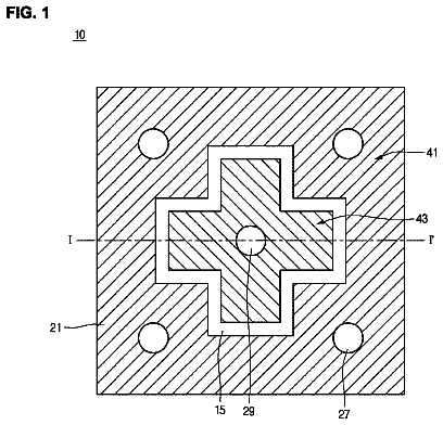
FIG. 1 is a plan view of a light emitting device according to an embodiment;
FIG. 2 is a sectional view taken along line I-I′ illustrated in FIG. 1 ;
FIG. 3 is a sectional view taken along line II-II′ illustrated in FIG. 1 ;
FIG. 4 is an enlarged sectional view of portion ‘A’ illustrated in FIG. 2 ;
FIG. 5 is an enlarged sectional view of portion ‘B’ illustrated in FIG. 2 ;
FIG. 6 is an enlarged sectional view of portion ‘C’ illustrated in FIG. 3 ;
FIG. 7 is a plan view of a light emitting device according to a comparative embodiment;
FIG. 8 is a sectional view taken along line III-III′ illustrated in FIG. 7 ; and
FIG. 9 is a sectional view of a light emitting device package according to an embodiment.
Description of specific embodiments
Hereinafter, exemplary embodiments will be described in detail with reference to the accompanying drawings to aid in understanding of the embodiments. However, the embodiments may be altered in various ways, and the scope of the embodiments should not be construed as limited to the following description. The embodiments are intended to provide those skilled in the art with more complete explanation.
In the following description of the embodiments, it will be understood that, when each element is referred to as being formed “on” or “under” the other element, it can be directly “on” or “under” the other element or be indirectly formed with one or more intervening elements therebetween. In addition, it will also be understood that “on” or “under” the element may mean an upward direction and a downward direction of the element.
In addition, the relative terms “first”, “second”, “top/upper/above”, “bottom/lower/under” and the like in the description and in the claims may be used to distinguish between any one substance or element and other substances or elements and not necessarily for describing any physical or logical relationship between the substances or elements or a particular order.
In the drawings, the thickness or size of each layer may be exaggerated, omitted or schematically illustrated for clarity and convenience. In addition, the size of each constituent element does not wholly reflect an actual size thereof.
FIG. 1 is a plan view of a light emitting device 100 according to an embodiment, FIG. 2 is a sectional view taken along line I-I′ illustrated in FIG. 1 , FIG. 3 is a sectional view taken along line II-II′ illustrated in FIG. 1 , FIG. 4 is an enlarged sectional view of portion ‘A’ illustrated in FIG. 2 , FIG. 5 is an enlarged sectional view of portion ‘B’ illustrated in FIG. 2 , and FIG. 6 is an enlarged sectional view of portion ‘C’ illustrated in FIG. 3 .
The light emitting device 100 according to the embodiment will be described below with reference to FIGS. 1 to 6 . FIG. 1 is a plan view illustrating the light emitting device 100 of FIG. 2 viewed in the +z-axis. For convenience of description, an insulation layer 150 and a contact layer 140 of the light emitting device 100 illustrated in FIGS. 2 to 6 are not illustrated in FIG. 1 .
The light emitting device 100 may include a substrate 110 , a light emitting structure 120 , a reflective layer 130 , a contact layer 140 , an insulation layer 150 , a transmissive conductive layer (or a transparent electrode) 160 , and first and second pads 172 and 174 .
The light emitting structure 120 may be displaced under the substrate 110 . The substrate 110 may comprise a conductive material or non-conductive material. For example, the substrate 110 may comprise at least one of sapphire (Al.sub.2O.sub.3), GaN, SiC, ZnO, GaP, InP, Ga.sub.2O.sub.3, GaAs, or Si, although the embodiment is not limited to the material of the substrate 110 .
In order to improve the difference in the Coefficient of Thermal Expansion (CTE) and the lattice mismatch between the substrate 110 and the light emitting structure 120 , a buffer layer (or a transition layer)(not illustrated) may be further disposed between the two 110 and 120 . The buffer layer, for example, may comprise at least one material selected from the group consisting of Al, In, N, and Ga, without being limited thereto. In addition, the buffer layer may have a single layer or multi-layer structure.
In addition, the substrate 110 illustrated in FIG. 1 may include a pattern 112 . Here, the pattern 112 may have any of various cross-sectional shapes in order to assist light, emitted from an active layer 124 , in escaping from the light emitting device 100 . For example, the substrate 110 may be a Patterned Sapphire Substrate (PSS).
The light emitting structure 120 may include a first conductive semiconductor layer 122 , the active layer 124 , and a second conductive semiconductor layer 126 , which are arranged in sequence under the substrate 110 .
The first conductive semiconductor layer 122 may be disposed under the substrate 110 , and may be implemented in, for example, group III-V or II-VI compound semiconductors doped with a first conductive dopant. When the first conductive semiconductor layer 122 is an n-type semiconductor layer, the first conductive dopant may be an n-type dopant, and comprise Si, Ge, Sn, Se, or Te, without being limited thereto.
For example, the first conductive semiconductor layer 122 may comprise a semiconductor material having a composition of Al.sub.xIn.sub.yGa(.sub.1−x−y)N (0≦x≦1, 0≦y≦1, 0≦x+y≦1). The first conductive semiconductor layer 122 may comprise any one or more materials selected from among GaN, InN, AlN, InGaN, AlGaN, InAlGaN, AlInN, AlGaAs, InGaAs, AlInGaAs, GaP, AlGaP, InGaP, AlInGaP, and InP.
The active layer 124 is disposed between the first conductive semiconductor layer 122 and the second conductive semiconductor layer 126 . The active layer 124 is a layer in which electrons (or holes) injected through the first conductive semiconductor layer 122 and holes (or electrons) injected through the second conductive semiconductor layer 126 meet each other to emit light having energy determined by an inherent energy band of a constituent material of the active layer 124 . The active layer 124 may be formed into at least one structure selected from among a single-well structure, a multi-well structure, a single-quantum well structure, a multi-quantum well structure, a quantum dot structure, and a quantum wire structure.
The active layer 124 may include a well layer and a barrier layer having a pair structure of any one or more of InGaN/GaN, InGaN/InGaN, GaN/AlGaN, InAlGaN/GaN, GaAs(InGaAs)/AlGaAs, and GaP(InGaP)/AlGaP, without being limited thereto. The well layer may be formed of a material having lower band gap energy than the band gap energy of the barrier layer.
A conductive clad layer (not illustrated) may be formed above and/or under the active layer 124 . The conductive clad layer may be formed of semiconductors having higher band gap energy than the band gap energy of the barrier layer of the active layer 124 . For example, the conductive clad layer may include GaN, AlGaN, InAlGaN, or an ultra lattice structure. In addition, the conductive clad layer may be doped with an n-type or p-type dopant.
In some embodiments, the active layer 124 may emit ultraviolet light having a specific wavelength band. Here, the ultraviolet light wavelength band may be within a range from 100 nm to 400 nm. In particular, the active layer 124 may emit light having a wavelength band within a range from 100 nm to 280 nm. However, the embodiment is not limited to the wavelength band of light emitted from the active layer 124 .
The second conductive semiconductor layer 126 may be disposed under the active layer 124 and may be formed of a semiconductor compound. The second conductive semiconductor layer 126 may be formed of, for example, group III-V or II-VI compound semiconductors. For example, the second conductive semiconductor layer 126 may comprise a semiconductor material having a composition of In.sub.xAl.sub.yGa.sub.1−x−yN (0≦x≦1, 0≦y≦1, 0≦x+y≦1). The second conductive semiconductor layer 126 may be doped with a second conductive dopant. When the second conductive semiconductor layer 126 is a p-type semiconductor layer, the second conductive dopant may be a p-type dopant and may include, for example, Mg, Zn, Ca, Sr, or Ba.
The first conductive semiconductor layer 122 may be an n-type semiconductor layer, and the second conductive semiconductor layer 126 may be a p-type semiconductor layer. Alternatively, the first conductive semiconductor layer 122 may be a p-type semiconductor layer, and the second conductive semiconductor layer 126 may be an n-type semiconductor layer.
The light emitting structure 120 may be implemented in any one structure selected from among an n-p junction structure, a p-n junction structure, an n-p-n junction structure, and a p-n-p junction structure.
Since the light emitting device 100 illustrated in FIGS. 1 to 6 has a flip chip bonding structure, and therefore light emitted from the active layer 124 may be emitted through the first conductive semiconductor layer 122 and the substrate 110 . To this end, the first conductive semiconductor layer 122 and the substrate 110 may be formed of a light transmissive material. At this time, although the second conductive semiconductor layer 126 may be formed of a transmissive or non-transmissive material, or a reflective material, the embodiment may not be limited to a specific material.
The reflective layer 130 may be disposed under the second conductive semiconductor layer 126 , and may have at least one first through-hole H 1 (e.g., H 1 - 1 to H 1 - 10 ) formed in a first direction (e.g., in the z-axis) that is the thickness direction of the light emitting structure 120 . The reflective layer 130 serves to reflect light that is emitted from the active layer 124 and directed to the first and second pads 172 and 174 .
To this end, the reflective layer 130 may be formed of a reflective material such as silver (Ag).
In addition, the at least one first through-hole H 1 (e.g., H 1 - 1 to H 1 - 10 ) may be located above at least one of the first or second pads 172 and 174 . For example, referring to FIGS. 1, 2, and 4 , the first through-holes H 1 - 1 , H 1 - 2 , and H 1 - 3 may be located above the first pad 172 . Referring to FIGS. 1, 2, and 5 , the first through-holes H 1 - 4 , H 1 - 5 , H 1 - 6 , and Hi- 7 may be located above the second pad 174 .
In addition, although a plurality of first through-holes H 1 may be provided, the embodiment is not limited as to the number of the first through-holes H 1 .
The respective first through-holes H 1 (e.g., H 1 - 1 to H 1 - 10 ) may have first widths W 1 in a second direction (e.g., in the x-axis), which may differ from one another, or may be the same. Here, although the second direction may be perpendicular to the first direction, the embodiment is not limited thereto.
For example, as exemplarily illustrated in FIG. 4 , the first through-holes H 1 - 1 , H 1 - 2 , and H 1 - 3 may have first widths W 11 , W 12 , and W 13 , respectively, which may be the same.
Alternatively, as exemplarily illustrated in FIG. 5 , the first through-holes H 1 - 4 , H 1 - 5 , H 1 - 6 , and H 1 - 7 may have first widths W 14 , W 15 , W 16 , and W 17 , respectively, which may differ from one another. In addition, as exemplarily illustrated in FIG. 6 , the first through-holes H 1 - 8 , H 1 - 9 , and H 1 - 10 may have first widths W 18 , W 19 , and W 20 , respectively, which may differ from one another.
In addition, the first through-holes H 1 may be spaced apart from one another by a constant distance, or by different distances.
For example, as exemplarily illustrated in FIG. 4 , the first through-holes H 1 - 1 , H 1 - 2 , and H 1 - 3 may be spaced apart from one another by the same distance (or gap) d 11 and d 12 .
Alternatively, as exemplarily illustrated in FIG. 5 , the first through-holes H 1 - 4 , H 1 - 5 , H 1 - 6 , and H 1 - 7 may be spaced apart from one another by different distances d 13 , d 14 , and d 15 . As exemplarily illustrated in FIG. 6 , the first through-holes H 1 - 8 , H 1 - 9 , and H 1 - 10 may be spaced apart from one another by different distances d 16 and d 17 .
In addition, although a plurality of second through-holes H 2 may be provided, the embodiment is not limited thereto. The at least one first through-hole H 1 may be located between the second through-holes H 2 .
In addition, the number of the at least one first through-holes H 1 , which are located between first ones of the second through-holes H 2 , may be different from or the same as the number of the at least one first through-holes H 1 which are located between second ones of the second through-holes H 2 .
As exemplarily illustrated in FIG. 1 , the same number of the first through-holes H 1 , for example, three first through-holes H 1 may be located between the respective second through-holes H 2 A- 1 to H 2 A- 8 and H 2 B- 1 to H 2 B- 7 . For example, referring to FIG. 1 , the number of the first through-holes H 1 - 1 , H 1 - 2 , and H 1 - 3 , located between first ones of the second through-holes H 2 , i.e. between the second through-holes H 2 A- 2 and H 2 A- 7 may be 3 , and the number of the first through-holes located between second ones of the second through-holes H 2 , i.e. between the second through-holes H 2 A- 2 and H 2 A- 3 may be 3 , which is the same as the number of the first through-holes H 1 - 1 , H 1 - 2 , and H 1 - 3 . As such, the number of the first through-holes H 1 located between the second through-holes H 2 A- 1 to H 2 A- 8 and H 2 B- 1 to H 2 B- 7 is the same.
However, although the number of the first through-holes H 1 - 1 , H 1 - 2 , and H 1 - 3 , located between the second through-holes H 2 A- 2 and H 2 A- 7 corresponding to first ones of the second through-holes H 2 is 3 as illustrated in FIG. 1 , the number of the first through-holes H 1 located between the second through-holes H 2 A- 2 and H 2 A- 3 corresponding to second ones of the second through-holes H 2 may be less than or greater than 3 unlike the illustration of FIG. 1 .
The contact layer 140 may be embedded in the at least one second through-hole H 2 (e.g., H 2 A- 1 to H 2 A- 8 and H 2 B- 1 to H 2 B- 7 ), which penetrate the reflective layer 130 , the second conductive semiconductor layer 126 , and the active layer 124 , so as to be electrically connected to the first conductive semiconductor layer 122 . As such, the contact layer 140 may be electrically connected to the first conductive semiconductor layer 122 via point contact.
Although the contact layer 140 may be implemented in the form of a penetration electrode, the embodiment is not limited thereto. That is, in another embodiment, although not illustrated, the contact layer 140 may bypass the reflective layer 130 , the second conductive semiconductor layer 126 , and the active layer 124 to thereby be electrically connected to the first conductive semiconductor layer 122 . As such, the contact layer 140 may serve as a first electrode.
The contact layer 140 may comprise an ohmic contact material, and serve as an ohmic layer. Thus, a separate ohmic layer (not illustrated) may be unnecessary, or a separate ohmic layer may be disposed above or under the contact layer 140 .
The contact layer 140 may reflect or transmit light emitted from the active layer 124 , rather than absorbing the light, and may be formed of any material that is capable of growing in good quality on the insulation layer 150 . For example, the contact layer 140 may be formed of a metal, and may be formed of Ag, Ni, Al, Rh, Pd, Ir, Ru, Mg, Zn, Pt, Au, Hf, and selective combinations thereof.
In addition, the first width W 1 of the at least one first through-hole H 1 (e.g., H 1 - 1 to H 1 - 10 ) in the second direction (e.g., in the x-axis), which is different from the first direction (e.g., in the z-axis), may be less than the second width W 2 of the at least one second through-hole H 2 (e.g., H 2 A- 1 to H 2 A- 8 and H 2 B- 1 to H 2 B- 7 ).
In addition, the transmissive conductive layer 160 may be disposed between the second conductive semiconductor layer 126 and the reflective layer 130 . The transmissive conductive layer 160 may be a Transparent Conductive Oxide (TCO) film. For example, the transmissive conductive layer 160 may comprise at least one of Indium Tin Oxide (ITO), Indium Zinc Oxide (IZO), Indium Zinc Tin Oxide (IZTO), Indium Aluminum Zinc Oxide (IAZO), Indium Gallium Zinc Oxide (IGZO), Indium Gallium Tin Oxide (IGTO), Aluminum Zinc Oxide (AZO), Antimony Tin Oxide (ATO), Gallium Zinc Oxide (GZO), IrOx, RuOx, RuOx/ITO, Ni/IrOx/Au, and Ni/IrOx/Au/ITO, and is not limited to these materials.
The reflective layer 130 and the transmissive conductive layer 160 may serve as a second electrode, and in some cases, the transmissive conductive layer 160 may be omitted.
The insulation layer 150 is disposed between the reflective layer 130 and the contact layer 140 , between the second conductive semiconductor layer 126 and the contact layer 140 , and between the active layer 124 and the contact layer 140 . Thus, each of the reflective layer 130 , the second conductive semiconductor layer 126 , and the active layer 124 may be electrically insulated from the contact layer 140 by the insulation layer 150 . In addition, when the transmissive conductive layer 160 is not omitted, the insulation layer 150 may be disposed between the transmissive conductive layer 160 and the contact layer 140 so as to electrically separate the two 160 and 140 from each other.
In addition, the insulation layer 150 may be embedded in the first through-hole H 1 (e.g., H 1 - 1 to H 1 - 10 ) formed in the reflective layer 130 .
The insulation layer 150 may extend in the second direction (e.g., in the x-axis), which is different from the first direction (e.g., in the z-axis), so as to be disposed between each of the first and second pads 172 and 174 and the contact layer 140 .
When the transmissive conductive layer 160 is omitted, the insulation layer 150 may be embedded in the first through-hole H 1 (e.g., H 1 - 1 to H 1 - 8 ) so as to be directly adhered to the second conductive semiconductor layer 126 . In this case, the insulation layer 150 may be formed of a material having stronger adhesion than adhesion between the reflective layer 130 and the second conductive semiconductor layer 126 . As such, since the adhesion between the insulation layer 150 and the second conductive semiconductor layer 126 is stronger than the adhesion between the reflective layer 130 and the second conductive semiconductor layer 126 , weak adhesion between the reflective layer 130 and the second conductive semiconductor layer 126 may be strengthened by the insulation layer 150 embedded in the first through-hole H 1 (e.g., H 1 - 1 to H 1 - 8 ).
Alternatively, when the transmissive conductive layer 160 is not omitted, the insulation layer 150 may be embedded in the first through-hole H 1 (e.g., H 1 - 1 to H 1 - 8 ) so as to be directly adhered to the transmissive conductive layer 160 . In this case, the insulation layer 150 may be formed of a material having stronger adhesion than adhesion between the reflective layer 130 and the transmissive conductive layer 160 . As such, weak adhesion between the reflective layer 130 and the transmissive conductive layer 160 may be strengthened by strong adhesion between the transmissive conductive layer 160 and the insulation layer 150 embedded in the first through-hole H 1 (e.g., H 1 - 1 to H 1 - 8 ).
As described above, the insulation layer 150 may be formed of a material which is capable of increasing adhesion between the reflective layer 130 and the insulation layer 150 beyond adhesion between the second conductive semiconductor layer 126 (or the transmissive conductive layer 160 ) and the reflective layer 130 .
The insulation layer 150 may be formed in a multi-layer structure of multiple layers or at least two layers, and may comprise at least one of SiO.sub.2, TiO.sub.2, ZrO.sub.2, Si.sub.3N.sub.4, Al.sub.2O.sub.3, or MgF.sub.2.
In addition, the insulation layer 150 may include a Distributed Bragg Reflector (DBR) or Omni-Directional Reflector (ODR). When the insulation layer 150 includes the DBR or ODR, the insulation layer 150 may perform both an insulation function and a reflection function.
The DBR may be configured in a manner such that a first layer (not illustrated) and a second layer (not illustrated), which have different indices of refraction, are alternately stacked one above another at least once. The DBR may be an electrical insulation material. For example, the first layer may include a first dielectric layer such as TiO.sub.2, and the second layer may include a second dielectric layer such as SiO.sub.2. For example, the DBR may take the form of a stack of at least one pair of TiO.sub.2/SiO.sub.2 layers. Each of the first layer and the second layer may have a thickness of λ/4, and λ may be the wavelength of light generated in a light emitting cell.
The ODR may be configured in such a manner that a low refractive index layer is formed on a metal reflective layer (not illustrated). The metal reflective layer may be formed of Ag or Al, and the low refractive index layer may be formed of a transparent material such as SiO.sub.2, Si.sub.3N.sub.4, or MgO. Alternatively, the ODR may take the form of a stack of pairs of a SiO.sub.2 layer and a TiO.sub.2 layer repeatedly stacked one above another, although the embodiment is not limited thereto.
Meanwhile, the first pad 172 may be disposed under the contact layer 140 so as to be electrically connected to the first conductive semiconductor layer 122 via the contact layer 140 . That is, since the first pad 172 may be electrically connected to the contact layer 140 as illustrated in FIG. 3 and the contact layer 140 may be electrically connected to the first conductive semiconductor layer 122 as illustrated in FIG. 2 , it will be appreciated that the first pad 172 is electrically connected to the first conductive semiconductor layer 122 via the contact layer 140 .
In addition, referring to FIG. 3 , it will be appreciated that the second pad 174 penetrates the insulation layer 150 so as to be electrically connected to the second conductive semiconductor layer 126 via the reflective layer 130 . Each of the first and second pads 172 and 174 may comprise an electrode material.
Hereinafter, the light emitting device according to the embodiment described above and a light emitting device according to a comparative embodiment in which the reflective layer 130 includes no first through-hole H 1 will be described with reference to the accompanying drawings.
FIG. 7 is a plan view of a light emitting device according to a comparative embodiment, and FIG. 8 is a sectional view taken along line illustrated in FIG. 7 .
The light emitting device according to the comparative embodiment illustrated in FIGS. 7 and 8 includes a substrate 10 , a light emitting structure 20 , a reflective layer 30 , a contact layer 40 , an insulation layer 50 , a transmissive electrode layer 60 , and first and second pads 72 and 74 .
The reflective layer 130 of the light emitting device 100 illustrated in FIGS. 1 to 6 has the first through-hole H 1 , and the insulation layer 150 is embedded in the first through-hole H 1 . On the other hand, in the light emitting device illustrated in FIGS. 7 and 8 , the reflective layer 30 has no first through-hole. As such, the light emitting device according to the comparative embodiment illustrated in FIGS. 7 and 8 is approximately the same as the light emitting device 100 illustrated in FIGS. 1 and 2 except that the configurations of the reflective layer 30 and the insulation layer 50 differ from the configurations of the reflective layer 130 and the insulation layer 150 illustrated in FIG. 1 . That is, the substrate 10 , the light emitting structure 20 , the contact layer 40 , the transmissive electrode layer 60 , and the first and second pads 72 and 74 respectively correspond to the substrate 110 , the light emitting structure 120 , the contact layer 140 , the transmissive conductive layer 160 , and the first and second pads 172 and 174 illustrated in FIGS. 1 and 2 , and thus perform the same functions and have the same configurations. In addition, a first conductive semiconductor layer 22 , an active layer 24 , and a second conductive semiconductor layer 26 illustrated in FIG. 8 respectively correspond to the first conductive semiconductor layer 122 , the active layer 124 , and the second conductive semiconductor layer 126 illustrated in FIG. 2 , and thus perform the same functions and have the same configurations.
The light emitting device according to the comparative embodiment illustrated in FIGS. 7 and 8 have no first through-hole H 1 of the light emitting device 100 according to the embodiment illustrated in FIGS. 1 to 6 . That is, the light emitting device according to the comparative embodiment has only the second through-hole H 2 illustrated in FIGS. 1 to 6 .
When the reflective layer 30 is formed of a metal material having high reflectance such as silver (Ag), the reflective layer 30 may peel off from the transmissive electrode layer 60 because of weak adhesion between the reflective layer 30 and the transmissive electrode layer 60 . This is because silver (Ag) has excellent reflectance, but has poor adhesion.
In addition, when the light emitting device according to the comparative embodiment illustrated in FIGS. 7 and 8 is flip-chip bonded to a package body which will be described below, peeling of a metal (e.g., silver (Ag)) may occur at the interface between the transmissive electrode layer 60 and the reflective layer 30 due to the difference between thermal expansion coefficients thereof.
However, in the case of the light emitting device 100 according to the embodiment in which the first through-hole H 1 is formed in the reflective layer 130 , the insulation layer 150 , which has higher adhesion with respect to the transmissive conductive layer 160 (or the second conductive semiconductor layer 126 when the transmissive conductive layer 160 is omitted) than a metal material such as silver (Ag), is embedded in the first through-hole H 1 . Thus, weak adhesion between the reflective layer 130 and the transmissive conductive layer 160 (or the second conductive semiconductor layer 126 when the transmissive conductive layer 160 is omitted) may be strengthened by the insulation layer 150 embedded in the first through-hole H 1 , and the metal peeling phenomenon described above may be prevented.
In addition, the first widths W 1 of the first through-holes H 1 in the second direction (e.g., in the x-axis) which is different from the first direction (e.g., in the z-axis) may increase with decreasing distance to the edge of the reflective layer 130 . In addition, the first widths W 1 of the first through-holes H 1 in the second direction (e.g., in the x-axis) which is different from the first direction (e.g., in the z-axis) may increase with decreasing distance to the edge of the light emitting structure 120 .
For example, referring to FIGS. 2 and 5 , it will be appreciated that the first widths W 17 , W 16 , W 15 , and W 14 of the first through-holes H 1 - 7 , H 1 - 6 , H 1 - 5 , and H 1 - 4 increase with decreasing distance to an edge 130 A of the reflective layer 130 . This may be represented by W 17 >W 16 >W 15 >W 14 . Likewise, referring to FIGS. 3 and 6 , it will be appreciated that the first widths W 18 , W 19 , and W 20 of the first through-holes H 1 - 8 , H 1 - 9 , and H 1 - 10 increase with decreasing distance to an edge 130 B of the reflective layer 130 . This may be represented by W 18 >W 19 >W 20 .
When the first widths W 1 of the first through-holes H 1 increase with decreasing distance to the edges 130 A and 130 B of the reflective layer 130 , the contact area between the insulation layer 150 and the transmissive conductive layer 160 (or the second conductive semiconductor layer 126 when the transmissive conductive layer 160 is omitted) increases. As such, the coupling force between the insulation layer 150 and the transmissive conductive layer 160 (or the second conductive semiconductor layer 126 when the transmissive conductive layer 160 is omitted) may be greater at the edges 130 A and 130 B than that at the center of the reflective layer 130 . Hence, even if the edge of the reflective layer 130 has lower adhesion and suffers from more frequent metal peeling than the center of the reflective layer 130 , it is possible to strengthen the low adhesion at the edge and thus prevent the metal peeling phenomenon.
In addition, the second through-holes H 2 may be divided into a plurality of second-first through-holes and second-second through-holes. The second-first through-holes may be defined as those second through-holes that are located closer to the edge than to the center of the light emitting structure 120 . In addition, the second-second through-holes may be defined as those through-holes that are located closer to the center than to the edge of the light emitting structure 120 . Referring to FIG. 1 , for example, the second-first through-holes H 2 A- 1 , H 2 A- 2 , H 2 A- 3 , H 2 A- 4 , H 2 A- 5 , H 2 A- 8 , H 2 B- 1 , H 2 B- 4 , H 2 B- 5 , H 2 B- 6 , and H 2 B- 7 are located closer to the edge than to the center of the light emitting structure 120 as compared to the second-second through-holes H 2 A- 6 , H 2 A- 7 , H 2 B- 2 , and H 2 B- 3 .
According to the embodiment, the number of the first through-holes H 1 , located between the second-first through-holes, may be greater than the number of the first through-holes H 1 located between the second-second through-holes.
In the case of FIG. 1 , the number of the first through-holes, located between the second-first through-holes H 2 A- 1 , H 2 A- 2 , H 2 A- 3 , H 2 A- 4 , H 2 A- 5 , H 2 A- 8 , H 2 B- 1 , H 2 B- 4 , H 2 B- 5 , H 2 B- 6 , and H 2 B- 7 , is 3 that is the same as the number of the first through-holes located between the second-second through-holes H 2 A- 6 , H 2 A- 7 , H 2 B- 2 , and H 2 B- 3 . However, unlike the illustration of FIG. 1 , the number of the first through-holes, located between the second-first through-holes H 2 A- 1 , H 2 A- 2 , H 2 A- 3 , H 2 A- 4 , H 2 A- 5 , H 2 A- 8 , H 2 B- 1 , H 2 B- 4 , H 2 B- 5 , H 2 B- 6 , and H 2 B- 7 , may be greater than the number of the first through-holes located between the second-second through-holes H 2 A- 6 , H 2 A- 7 , H 2 B- 2 , and H 2 B- 3 . As the number of the first through-holes increases, the contact area between the insulation layer 150 and the transmissive conductive layer 160 (or the second conductive semiconductor layer 126 when the transmissive conductive layer 160 is omitted) increases. Thus, the coupling force between the insulation layer 150 and the transmissive conductive layer 160 (or the second conductive semiconductor layer 126 when the transmissive conductive layer 160 is omitted) becomes greater at the edge than that at the center of the light emitting structure 120 . Hence, even if the reflective layer 130 has lower adhesion and suffers from more frequent metal peeling at the edge of the light emitting structure 120 than the center of the light emitting structure 120 , it is possible to strengthen the low adhesion and thus prevent the metal peeling phenomenon.
In addition, when the first widths W 1 (e.g., W 11 to W 20 ) of the at least one first through-holes H 1 in the second direction (e.g., in the x-axis), which is different from the first direction (e.g., in the z-axis), are below 5 μm, the adhesion between the insulation layer 150 embedded in the first through-holes H 1 and the transmissive conductive layer 160 (or the second conductive semiconductor layer 126 when the transmissive conductive layer 160 is omitted) may not be great. Alternatively, when the first widths W 1 (e.g., W 11 to W 20 ) are above 30 μm, the amount of carrier, injected into the second conductive semiconductor layer 126 by way of the reflective layer 130 from the second pad 174 , may be reduced, resulting in deterioration in light emission efficiency. Accordingly, the first widths W 1 (e.g., W 11 to W 20 ) may be within a range from 5 μm to 30 μm, although the embodiment is not limited thereto.
The description continues in the full USPTO document.
 Lapsed, fee not paid7 drawings