 Lapsed, fee not paid20 drawings
Cameras, Displays & Optics · US 9,784,982 B2
Stereoscopic display device
A configuration of a stereoscopic display device that is capable of maintaining crosstalk at a low level even when a viewer moves is provided.
US 9,785,006 B2 · Assignee: Sony Corporation · Inventors: Shinkai; Shogo et al.
Sheet 1 of 66 from the published document. All sheets in the USPTO PDF
An illumination unit of an embodiment of the present technology includes: an illumination optical system configured to generate illumination light; and a plurality of lenses configured to reduce a divergence angle of the illumination light. The illumination optical system includes: a light source ( 20 ) configured to apply light onto an end surface of one of a first substrate and a second substrate; and a light modulation layer ( 30 ) provided in a gap between the first substrate and the second substrate. The illumination optical system includes an electrode configured to generate an electric filed that generates, in the light modulation layer ( 30 ), a plurality of linear scattering regions ( 30 B) in a three-dimensional mode, and to generate an electric field that generates, in the light modulation layer, a planar scattering region in a two-dimensional display mode. The lenses are arranged side by side in a direction in which the linear scattering regions extend, and are also arranged side by side in a direction intersecting with the direction in which the linear scattering regions extend.
Some display apparatuses capable of performing three-dimensional display require to wear eyeglasses dedicated therefor, and the others require no eyeglasses dedicated therefor. The latter display apparatuses use a lenticular lens, a parallax barrier, etc. in order to allow a stereoscopic picture to be perceived with naked eyes. Picture information is thus distributed to left and right eyes, and different pictures are thereby viewed between the left and right eyes. As a result, three-dimensional display is achieved. By the way, in a case where a physical barrier is provided in the display apparatus that is capable of allowing a stereoscopic picture to be perceived with naked eyes, it is necessary to provide a switchable diffuser between the bather and a display panel. Patent Document 1 proposes a way to provide a simple configuration with using such a diffuser. PRIOR ART DOCUMENT Patent D
1 of 66 drawing sheets so far from the published document, cropped to the drawing. Every sheet is in the USPTO PDF.
What the patent claimed, word for word. All of it is now free to use.
The present technology relates to a display apparatus that is capable of performing two-dimensional display (planar display) and three-dimensional display (stereoscopic display), and to an illumination unit suitably applicable as a backlight of such a display apparatus.
Some display apparatuses capable of performing three-dimensional display require to wear eyeglasses dedicated therefor, and the others require no eyeglasses dedicated therefor. The latter display apparatuses use a lenticular lens, a parallax barrier, etc. in order to allow a stereoscopic picture to be perceived with naked eyes. Picture information is thus distributed to left and right eyes, and different pictures are thereby viewed between the left and right eyes. As a result, three-dimensional display is achieved.
By the way, in a case where a physical barrier is provided in the display apparatus that is capable of allowing a stereoscopic picture to be perceived with naked eyes, it is necessary to provide a switchable diffuser between the bather and a display panel. Patent Document 1 proposes a way to provide a simple configuration with using such a diffuser. PRIOR ART DOCUMENT Patent Document
Patent Document 1: Japanese Unexamined Patent Application Publication No. 2007-519033 SUMMARY OF THE INVENTION
However, in Patent Document 1, a polarization-dependent scatterer is used as the diffuser, and a polarizer is further used for causing polarized light to enter the polarization-dependent scatterer. This has caused an issue that light is absorbed by the polarizer, which results in decrease in display luminance.
Accordingly, it is desirable to provide an illumination unit capable of achieving high luminance and a display apparatus including the illumination unit.
An illumination unit of an embodiment of the present technology is used as an illumination unit that is allowed to output illumination light in a display apparatus provided with a display panel configured to modulate the illumination light based on a picture signal and thereby generate picture light. The illumination unit of an embodiment of the present technology includes an illumination optical system configured to generate the illumination light, and a plurality of lenses configured to reduce a divergence angle of the illumination light. The illumination optical system includes a first substrate and a second substrate arranged to be separated from each other and to be opposed to each other, and a light source configured to apply light onto an end surface of one of the first substrate and the second substrate. The illumination optical system also includes a light modulation layer provided in a gap between the first substrate and the second substrate and configured to exhibit scattering characteristics or transparent characteristics, with respect to the light from the light source, depending on magnitude of an electric field. The illumination optical system also includes an electrode configured to generate an electric filed that generates, in the light modulation layer, a plurality of linear scattering regions or a plurality of first dot-like scattering regions in a three-dimensional display mode, and to generate an electric field that generates, in the light modulation layer, a planar scattering region or a plurality of second dot-like scattering regions in a two-dimensional display mode, the first dot-like scattering regions being arranged side by side in a plurality of lines, and the second dot-like scattering regions being arranged side by side in a matrix. The lenses are arranged side by side in one of a direction in which the linear scattering regions extend, a direction in which a plurality of the first dot-like scattering regions are arranged side by side in a line, and a direction in which a plurality of the second dot-like scattering regions are arranged side by side in a line. The lenses are also arranged side by side in a direction intersecting with one of the direction in which the linear scattering regions extend, the direction in which the plurality of first dot-like scattering regions are arranged side by side in the line, and the direction in which the plurality of second dot-like scattering regions are arranged side by side in the line.
A display apparatus of an embodiment of the present technology includes an illumination unit allowed to output illumination light, and a display panel configured to modulate the illumination light based on a picture signal and thereby generate picture light. The illumination unit mounted on the display apparatus has a configuration similar to the configuration of the illumination unit of the embodiment described above.
In the illumination unit and the display apparatus of embodiments of the present technology, the light modulation layer that exhibits the scattering characteristics or the transparent characteristics, with respect to the light from the light source, depending on magnitude of an electric field is provided in the illumination unit. Accordingly, light that is emitted from the light source and propagates through the first substrate, etc. passes through a region, in the light modulation layer, that exhibits the transparent characteristics in response to control of the electric field, and is reflected totally or at high reflectance at a top surface of the illumination unit. As a result, luminance in a region (hereinafter, simply referred to as “transparent region in light exiting region”) corresponding to a region, of the light exiting region of the illumination unit, that exhibits the transparent characteristics is decreased compared to in a case where the entire surface is caused to emit light uniformly. On the other hand, the light that propagates through the first substrate, etc. is scattered in a region, of the light modulation layer, that exhibits the scattering characteristics in response to the control of the electric field, and passes through the top surface of the illumination unit. As a result, luminance in a region (hereinafter, simply referred to as “scattering region in the light exiting region”) corresponding to a region, of the light exiting region of the illumination unit, that exhibits the scattering characteristics is increased compared to in the case where the entire surface is caused to emit light uniformly. Moreover, luminance in partial white display (increase in luminance) is increased as the luminance in the transparent region in the light exiting region is decreased. In an embodiment of the present technology, a plurality of linear scattering regions or a plurality of first dot-like scattering regions that are arranged side by side in a plurality of lines are generated in the light modulation layer in the three-dimensional display mode. In an embodiment of the present technology, a planar scattering region or a plurality of second dot-like scattering regions that are arranged side by side in a matrix are generated in the light modulation layer in the two-dimensional display mode. At the time of performing three-dimensional display, the light from the light source is utilized to cause a plurality of linear light rays (or a plurality of linear light rays formed of a plurality of dot-like illumination light rays that are arranged side by side in a line) to exit from the light modulation layer. On the other hand, at the time of performing two-dimensional display, the light from the light source is utilized to cause planar light ray (or a planar light formed of a plurality of dot-like illumination light rays that are arranged side by side in a line) to exit from the light modulation layer. In such a manner, in an embodiment of the present technology, it is possible to perform switching between three-dimensional display and two-dimensional display without using a physical barrier, a polarizer, etc. Moreover, in an embodiment of the present technology, the plurality of lenses configured to reduce the divergence angle of the illumination light is provided in the illumination unit. The lenses are arranged side by side in one of the direction in which the linear scattering regions extend, the direction in which the plurality of first dot-like scattering regions are arranged side by side in the line, and the direction in which the plurality of second dot-like scattering regions are arranged side by side in the line. The lenses are also arranged side by side in the direction intersecting with one of the direction in which the linear scattering regions extend, the direction in which the plurality of first dot-like scattering regions are arranged side by side in the line, and the direction in which the plurality of second dot-like scattering regions are arranged side by side in the line. Accordingly, it is possible to increase an amount of light that enters the display panel at an appropriate viewing angle, compared to in a case where the lenses are not provided.
According to the illumination unit and the display apparatus according to embodiments of the present technology, it is possible to perform switching between three-dimensional display and two-dimensional display without using a physical barrier, a polarizer, etc., and it is also possible to increase amount of light that enters the display panel at an appropriate viewing angle. As a result, it is possible to achieve high luminance in a displayed picture.
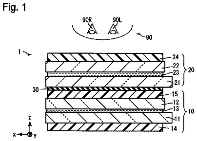
FIG. 1 is a diagram illustrating a cross-sectional configuration example of an illumination unit according to a first embodiment of the present technology.
FIG. 2 is a diagram illustrating a cross-sectional configuration example of a light modulation device illustrated in FIG. 1 .
FIG. 3 is a diagram illustrating a planar configuration example of a bottom electrode illustrated in FIG. 2 .
FIG. 4A is a diagram schematically illustrating an example of a function of a light modulation layer illustrated in FIG. 2 .
FIG. 4B is a diagram illustrating an example of optical characteristics of a bulk and a microparticle illustrated in FIG. 4A .
FIG. 4C is a diagram schematically illustrating a state in which light passes through a light modulation layer illustrated in FIG. 4A .
FIG. 5A is a diagram schematically illustrating another example of the function of the light modulation layer illustrated in FIG. 2 .
FIG. 5B is a diagram illustrating an example of optical characteristics of a bulk and a microparticle illustrated in FIG. 5A .
FIG. 5C is a diagram schematically illustrating a state in which light passes through a light modulation layer illustrated in FIG. 5A .
FIG. 6 is a diagram schematically illustrating an example of a function of the illumination unit illustrated in FIG. 1 .
FIG. 7 is a diagram illustrating a perspective configuration example of a lens sheet illustrated in FIG. 1 .
FIG. 8 is a diagram illustrating another example of the perspective configuration of the lens sheet illustrated in FIG. 1 .
FIG. 9A is a diagram illustrating an example of a curved surface shape of a convex portion illustrated in FIGS. 7 and 8 .
FIG. 9B is a diagram illustrating another example of the curved surface shape of the convex portion illustrated in FIGS. 7 and 8 .
FIG. 10 is a diagram illustrating a cross-sectional configuration example of a lens sheet illustrated in FIG. 7 , together with a light guide plate and the light modulation device.
FIG. 11 is a diagram illustrating a cross-sectional configuration example of a lens sheet illustrated in FIG. 8 , together with the light guide plate and the light modulation device.
FIG. 12 is a diagram illustrating a first modification of the cross-sectional configuration example of the lens sheet illustrated in FIG. 7 , together with the light guide plate and the light modulation device.
FIG. 13 is a diagram illustrating a first modification of the cross-sectional configuration example of the lens sheet illustrated in FIG. 8 , together with the light guide plate and the light modulation device.
FIG. 14 is a diagram illustrating a second modification of the cross-sectional configuration example of the lens sheet illustrated in FIG. 7 , together with the light guide plate and the light modulation device.
FIG. 15 is a diagram illustrating a second modification of the cross-sectional configuration example of the lens sheet illustrated in FIG. 8 , together with the light guide plate and the light modulation device.
FIG. 16 is a diagram illustrating a third modification of the cross-sectional configuration example of the lens sheet illustrated in FIG. 7 , together with the light guide plate and the light modulation device.
FIG. 17 is a diagram illustrating a third modification of the cross-sectional configuration example of the lens sheet illustrated in FIG. 8 , together with the light guide plate and the light modulation device.
FIG. 18 is a diagram illustrating an example of a positional relationship between the convex portions of the lens sheet illustrated in FIGS. 7 and 8 and partial electrodes of the bottom electrode illustrated in FIG. 3 .
FIG. 19 is a diagram illustrating a fourth modification of the cross-sectional configuration example of the lens sheet illustrated in FIG. 7 , together with the light guide plate and the light modulation device.
FIG. 20 is a diagram illustrating a fourth modification of the cross-sectional configuration example of the lens sheet illustrated in FIG. 8 , together with the light guide plate and the light modulation device.
FIG. 21 is a diagram illustrating a fifth modification of the cross-sectional configuration example of the lens sheet illustrated in FIG. 7 , together with the light guide plate and the light modulation device.
FIG. 22 is a diagram illustrating a fifth modification of the cross-sectional configuration example of the lens sheet illustrated in FIG. 8 , together with the light guide plate and the light modulation device.
FIG. 23 is a diagram illustrating a sixth modification of the cross-sectional configuration example of the lens sheet illustrated in FIG. 7 , together with the light guide plate and the light modulation device.
FIG. 24 is a diagram illustrating a sixth modification of the cross-sectional configuration example of the lens sheet illustrated in FIG. 8 , together with the light guide plate and the light modulation device.
FIG. 25 is a diagram illustrating a seventh modification of the cross-sectional configuration example of the lens sheet illustrated in FIG. 7 , together with the light guide plate and the light modulation device.
FIG. 26 is a diagram illustrating a seventh modification of the cross-sectional configuration example of the lens sheet illustrated in FIG. 8 , together with the light guide plate and the light modulation device.
FIG. 27 is a diagram illustrating a first modification of the bottom electrode illustrated in FIG. 2 .
FIG. 28A is a diagram illustrating an example of a positional relationship between the convex portions of the lens sheet illustrated in FIGS. 7 and 8 and partial electrodes of a bottom electrode illustrated in FIG. 27 .
FIG. 28B is a diagram illustrating another example of the positional relationship between the convex portions of the lens sheet illustrated in FIGS. 7 and 8 and the partial electrodes of the bottom electrode illustrated in FIG. 27 .
FIG. 29 is a diagram illustrating a second modification of the bottom electrode illustrated in FIG. 2 .
FIG. 30 is a diagram illustrating an example of a positional relationship between the convex portions of the lens sheet illustrated in FIGS. 7 and 8 and partial electrodes of a bottom electrode illustrated in FIG. 29 .
FIG. 31 is a diagram illustrating a third modification of the bottom electrode illustrated in FIG. 2 .
FIG. 32 is a diagram illustrating an example of a positional relationship between the convex portions of the lens sheet illustrated in FIGS. 7 and 8 and partial electrodes of a bottom electrode illustrated in FIG. 31 .
FIG. 33 is a diagram illustrating a fourth modification of the bottom electrode illustrated in FIG. 2 .
FIG. 34A is a diagram illustrating an example of a positional relationship between the convex portions of the lens sheet illustrated in FIGS. 7 and 8 and partial electrodes of a bottom electrode illustrated in FIG. 33 .
FIG. 34B is a diagram illustrating another example of the positional relationship between the convex portions of the lens sheet illustrated in FIGS. 7 and 8 and the partial electrodes of the bottom electrode illustrated in FIG. 33 .
FIG. 35 is a diagram illustrating a fifth modification of the bottom electrode illustrated in FIG. 2 .
FIG. 36 is a diagram illustrating an example of a positional relationship between the convex portions of the lens sheet illustrated in FIGS. 7 and 8 and partial electrodes of a bottom electrode illustrated in FIG. 35 .
FIG. 37 is a diagram illustrating a sixth modification of the bottom electrode illustrated in FIG. 2 .
FIG. 38 is a diagram illustrating a first modification of the cross-sectional configuration of the light modulation device illustrated in FIG. 1 .
FIG. 39 is a diagram illustrating a planar configuration example of a top electrode illustrated in FIG. 38 .
FIG. 40 is a diagram illustrating a first modification of the top electrode illustrated in FIG. 38 .
FIG. 41 is a diagram illustrating a second modification of the top electrode illustrated in FIG. 38 .
FIG. 42 is a diagram illustrating a third modification of the top electrode illustrated in FIG. 38 .
FIG. 43 is a diagram illustrating a fourth modification of the top electrode illustrated in FIG. 38 .
FIG. 44 is a diagram illustrating a fifth modification of the top electrode illustrated in FIG. 38 .
FIG. 45 is a diagram illustrating a second modification of the cross-sectional configuration of the light modulation device illustrated in FIG. 1 .
FIG. 46 is a diagram illustrating a planar configuration example of a top electrode illustrated in FIG. 45 .
FIG. 47 is a diagram illustrating a planar configuration example of a bottom electrode illustrated in FIG. 45 .
FIG. 48 is a diagram illustrating a first modification of a combination of the top electrode and the bottom electrode illustrated in FIG. 45 .
FIG. 49 is a diagram illustrating a second modification of the combination of the top electrode and the bottom electrode illustrated in FIG. 45 .
FIG. 50 is a diagram illustrating a third modification of the combination of the top electrode and the bottom electrode illustrated in FIG. 45 .
FIG. 51 is a diagram illustrating a fourth modification of the combination of the top electrode and the bottom electrode illustrated in FIG. 45 .
FIG. 52 is a diagram illustrating a fifth modification of the combination of the top electrode and the bottom electrode illustrated in FIG. 45 .
FIG. 53 is a diagram illustrating a sixth modification of the combination of the top electrode and the bottom electrode illustrated in FIG. 45 .
FIG. 54 is a diagram illustrating a seventh modification of the combination of the top electrode and the bottom electrode illustrated in FIG. 45 .
FIG. 55 is a diagram illustrating an eighth modification of the combination of the top electrode and the bottom electrode illustrated in FIG. 45 .
FIG. 56A is a diagram illustrating a modification of the bottom electrode illustrated in FIGS. 2 and 33 .
FIG. 56B is a diagram illustrating another modification of the bottom electrode illustrated in FIGS. 2 and 33 .
FIG. 57A is a diagram illustrating a modification of the top electrode illustrated in FIGS. 2 and 43 .
FIG. 57B is a diagram illustrating another modification of the top electrode illustrated in FIGS. 2 and 43 .
FIG. 58 is a diagram illustrating a first modification of the cross-sectional configuration of the illumination unit illustrated in FIG. 1 .
FIG. 59 is a diagram illustrating a second modification of the cross-sectional configuration of the illumination unit illustrated in FIG. 1 .
FIG. 60 is a diagram illustrating an example of ends of the bottom electrode illustrated in FIGS. 2 and 45 and the top electrode illustrated in FIGS. 38 and 45 .
FIG. 61 is a diagram illustrating another example of the ends of the bottom electrode illustrated in FIGS. 2 and 45 and the top electrode illustrated in FIGS. 38 and 45 .
FIG. 62 is a diagram illustrating an example of pattern density distribution in the electrode.
FIG. 63 is a diagram illustrating a first modification of the pattern density distribution in the electrode.
FIG. 64 is a diagram illustrating a second modification of the pattern density distribution in the electrode.
FIG. 65 is a diagram illustrating a third modification of the pattern density distribution in the electrode.
FIG. 66 is a diagram illustrating, in a graph, the pattern density distribution in the electrode.
FIG. 67 is a diagram illustrating an example of luminance distribution in a case where the electrode having the pattern density illustrated in FIG. 66 is used.
FIG. 68 is a schematic diagram for describing an example of a function of the light modulation device.
FIG. 69 is a schematic diagram for describing another example of the function of the light modulation device.
FIG. 70 is a schematic diagram for describing still another example of the function of the light modulation device.
FIG. 71A is a perspective view illustrating an example of a configuration of a light source illustrated in FIG. 1 .
FIG. 71B is a perspective view illustrating another example of the configuration of the light source illustrated in FIG. 1 .
FIG. 71C is a perspective view illustrating still another example of the configuration of the light source illustrated in FIG. 1 .
FIG. 72A is a perspective view illustrating an example of a configuration of the light guide plate illustrated in FIG. 1 .
FIG. 72B is a perspective view illustrating another example of the configuration of the light guide plate illustrated in FIG. 1 .
FIG. 73A is a perspective view illustrating another example of the configuration of the light guide plate illustrated in FIG. 1 .
FIG. 73B is a cross-sectional view illustrating an example of a configuration of a light guide plate illustrated in FIG. 73A .
FIG. 74A is a schematic diagram illustrating an example of a function of the light guide plate illustrated in FIGS. 72 and 73 .
FIG. 74B is a schematic diagram illustrating another example of the function of the light guide plate illustrated in FIGS. 72 and 73 .
FIG. 75 is a diagram illustrating a modification of the bottom electrode and the top electrode.
FIG. 76 is a diagram illustrating a modification of the bottom electrode and the top electrode.
FIG. 77 is a diagram illustrating a modification of the bottom electrode and the top electrode.
FIG. 78 is a diagram illustrating a modification of the bottom electrode and the top electrode.
FIG. 79 is a diagram illustrating, in a graph, pattern density distribution of the electrode.
FIG. 80 is a diagram illustrating an example of luminance distribution in a case where the electrode having the pattern density illustrated in FIG. 79 is used.
FIG. 81 is a diagram illustrating a modification of the bottom electrode.
FIG. 82 is a diagram illustrating a modification of the bottom electrode.
FIG. 83 is a diagram illustrating a modification of the bottom electrode.
FIG. 84 is a diagram illustrating a modification of the bottom electrode.
FIG. 85 is a diagram illustrating a modification of the bottom electrode.
FIG. 86 is a diagram illustrating a modification of the bottom electrode.
FIG. 87 is a diagram illustrating a modification of the bottom electrode.
FIG. 88 is a diagram illustrating a first modification of the cross-sectional configuration of the light modulation device illustrated in FIG. 1 .
FIG. 89 is a diagram illustrating a second modification of the cross-sectional configuration of the light modulation device illustrated in FIG. 1 .
FIG. 90 is a diagram illustrating a third modification of the cross-sectional configuration of the light modulation device illustrated in FIG. 1 .
FIG. 91 is a diagram illustrating a third modification of the cross-sectional configuration of the illumination unit illustrated in FIG. 1 .
FIG. 92 is a diagram illustrating an example of a receiving-transmitting system of a television broadcast signal according to a second embodiment of the present technology.
FIG. 93 is a diagram illustrating an example of a functional block of a receiver apparatus illustrated in FIG. 92 .
FIG. 94 is a diagram illustrating a cross-sectional configuration example of a display section in the receiver apparatus illustrated in FIG. 92 .
FIG. 95 is a perspective view illustrating an example of a relationship between a rubbing direction in the display section and a transmission axis of a polarizing plate illustrated in FIG. 94 .
FIG. 96 is a perspective view illustrating another example of the relationship between the rubbing direction in the display section and the transmission axis of the polarizing plate illustrated in FIG. 94 .
FIG. 97 is a schematic diagram for describing three-dimensional display in the display section illustrated in FIG. 94 .
FIG. 98 is a schematic diagram for describing two-dimensional display in the display section illustrated in FIG. 94 .
FIG. 99 is a cross-sectional view illustrating a first modification of the lens sheet.
FIG. 100 is a cross-sectional view illustrating a second modification of the lens sheet.
FIG. 101 is a cross-sectional view illustrating a first modification of the display section illustrated in FIG. 94 .
FIG. 102 is a cross-sectional view illustrating a second modification of the display section illustrated in FIG. 94 .
FIG. 103 is a diagram illustrating a cross-sectional configuration example of a parallax bather.
FIG. 104 is a schematic diagram illustrating a cross-sectional configuration example of a display section illustrated in FIG 101 .
FIG. 105 is a schematic diagram illustrating an example of a relationship between pixels in a display panel and light from a backlight.
FIG. 106A is a schematic diagram illustrating an example of the light from the backlight.
FIG. 106B is a schematic diagram illustrating an example of a relationship between pixels in the display panel and the light from the backlight illustrated in FIG. 106A .
FIG. 107A is a schematic diagram illustrating another example of the light from the backlight.
FIG. 107B is a schematic diagram illustrating an example of a relationship between the pixels in the display panel and light from a backlight illustrated in FIG. 107A .
FIG. 108 is a schematic diagram illustrating an example of time-divisional drive in three-dimensional display.
FIG. 109 is a schematic diagram illustrating an example of the time-divisional drive following that illustrated in FIG. 108 .
FIG. 110 is a schematic diagram illustrating an example of the time-divisional drive following that illustrated in FIG. 109 .
FIG. 111 is a schematic diagram illustrating an example of the time-divisional drive following that illustrated in FIG. 110 .
FIG. 112 is a cross-sectional view illustrating a fifth modification of the display section illustrated in FIG. 94 .
FIG. 113 is a cross-sectional view illustrating a sixth modification of the display section illustrated in FIG. 94 .
Some embodiments of the invention are described below in detail with reference to the drawings. Incidentally, the description is provided in the following order. 1. First Embodiment (Illumination Unit) 2. Modifications of First Embodiment (Illumination Unit) 3. Second Embodiment (Receiver Apparatus) 4. Modifications of Second Embodiment (Receiver Apparatus) 5. Examples
[1. First Embodiment]
FIG. 1 illustrates a cross-sectional configuration of an illumination unit 1 according to a first embodiment of the present technology. The illumination unit 1 is applicable as a backlight of a display apparatus, and is allowed to output illumination light. The illumination unit 1 may include, for example, a light guide plate 10 , a light source 20 , a light modulation device 30 , a reflection plate 40 , a lens sheet 50 , and a drive circuit 60 . The light source 20 may be arranged on a side surface of the light guide plate 10 . The light modulation device 30 may be arranged inside the light guide plate 10 . The reflection plate 40 may be arranged on the back of the light guide plate 10 . The lens sheet 50 may be arranged above the light guide plate 10 . The drive circuit 60 may drive the light modulation device 30 .
It is to be noted that the light guide plate 10 corresponds to a specific example of “first substrate” or “second substrate” in the present technology. The light source 20 corresponds to a specific example of “light source” in the present technology. An optical system configured of the light source 20 , the light modulation device 30 , and the reflection plate 40 corresponds to a specific example of “illumination optical system” in the present technology.
(Light Guide Plate 10 )
The light guide plate 10 guides light from the light source 20 arranged on the side surface of the light guide plate 10 toward a top surface of the light guide plate 10 (specifically, a light exiting surface 1 A of the illumination unit 1 ). The light guide plate 10 may have, for example, a shape corresponding to a subject to be illuminated (for example, a display panel 210 which is described later) that is arranged on the top surface of the light guide plate 10 . For example, the light guide plate 10 may have a cuboid shape that is surrounded by a top surface, a bottom surface, and side surfaces. It is to be noted that, out of the side surfaces of the light guide plate 10 , the side surface which the light from the light source 20 enters is referred to as a light entering surface 10 A below.
The light guide plate 10 may have, for example, a shape having a predetermined pattern on one or both of the top surface and the bottom surface. The light guide plate 10 may have, for example, a function of scattering and uniformizing light entered from the light entering surface 10 A. It is to be noted that, in a case where luminance is uniformized by modulating a voltage to be applied to the light modulation device 30 , a flat light guide plate that has not been patterned may be used as the light guide plate 10 . The light guide plate 10 may be, for example, a transparent substrate that mainly includes a transparent thermoplastic resin such as a polycarbonate resin (PC) or an acrylic resin (polymethylmethacrylate (PMMA)).
(Light Source 20 )
The light source 20 is a linear light source, and may be configured, for example, of a hot cathode fluorescent lamp (HCFL), a cold cathode fluorescent lamp (CCFL), a plurality of LEDs (Light Emitting Diodes) arranged in a line, or the like. In a case where the light source 20 is configured of the plurality of LEDs, all of the LEDs may be preferably configured of white LEDs in view of efficiency, reduction in thickness, and uniformity. It is to be noted that, the light source 20 may include a red LED, a green LED, and a blue LED, for example. The light source 20 may be provided only on one side surface of the light guide plate 10 (see FIG. 1 ), or may be provided on two side surfaces, three side surfaces, or all of the side surfaces of the light guide plate 10 .
(Light Modulation Device 30 )
In the present embodiment, the light modulation device 30 is closely attached to inside of the light guide plate 10 with no air layer in between. The light modulation device 30 may be adhered to the light guide plate 10 with an adhesive (not illustrated) in between, for example. As illustrated in FIG. 2 , the light modulation device 30 may include, for example, a transparent substrate 31 , a bottom electrode 32 , an alignment film 33 , a light modulation layer 34 , an alignment film 35 , a top electrode 36 , and a transparent substrate 37 that are arranged in order from the reflection plate 40 . It is to be noted that FIG. 2 illustrates a cross-sectional configuration example of the light modulation device 30 . The bottom electrode 32 and the top electrode 36 correspond to a specific example of “electrode” in the present technology. The light modulation layer 34 corresponds to a specific example of “light modulation layer” in the present technology.
The transparent substrates 31 and 37 are arranged to be separated from each other and to be opposed to each other. The transparent substrates 31 and 37 support the light modulation layer 34 . Generally, each of the transparent substrates 31 and 37 may be configured of a substrate transparent with respect to visible light such as a glass plate or a plastic film. The top electrode 36 and the bottom electrode 32 are configured to generate an electric field that generates, in the light modulation layer 34 , a plurality of dot-like scattering regions that are arranged side by side in a plurality of lines or a plurality of linear scattering regions in a three-dimensional mode. Further, the top electrode 36 and the bottom electrode 32 are configured to generate an electric field that generates, in the light modulation layer 34 , a planar scattering region or a plurality of dot-like scattering regions that are arranged side by side in a matrix in a two-dimensional display mode. It is to be noted that the linear scattering region, the dot-like scattering region, and the planar scattering region are described in detail when description of the light modulation layer 34 is provided.
The top electrode 36 is provided on a surface, of the transparent substrate 37 , that is opposed to the transparent substrate 31 . The top electrode 36 may be configured, for example, of one sheet-like electrode (continuous film) that is formed over the entire inside of the surface. On the other hand, the bottom electrode 32 is provided on a surface, of the transparent substrate 31 , that is opposed to the transparent substrate 37 . As illustrated in FIGS. 2 and 3 , the bottom electrode 32 may be configured, for example, of a plurality of partial electrodes 32 A. It is to be noted that FIG. 3 illustrates a planar configuration example of the bottom electrode 32 .
As illustrated in FIG. 3 , each of the partial electrodes 32 A may have a block shape, and the partial electrodes 32 A may be arranged in a matrix, for example. The partial electrodes 32 A may be arranged side by side in a direction parallel to the light entering surface 10 A, and may be also arranged side by side in a direction orthogonal to the light entering surface 10 A, for example. When a plurality of partial electrodes 32 A that are arranged side by side in a line in the direction parallel to the light entering surface 10 A, out of the two arrangement directions of the partial electrodes 32 A, are considered one linear electrode 32 D, an arrangement direction (direction orthogonal to the light entering surface 10 A) of the linear electrode 32 D corresponds to a parallax direction at the time of performing three-dimensional display.
The bottom electrode 32 is configured to generate an electric field that generates, with respect to the light modulation layer 34 , a plurality of lines of linear scattering regions (or a plurality of dot-like scattering regions that are arranged side by side in a line), when three-dimensional display is performed in the display apparatus (in the three-dimensional display mode). A plurality of specific linear electrodes 32 D (hereinafter, referred to as “linear electrodes 32 B”) out of the linear electrodes 32 D are configured to generate an electric field that generates, in the light modulation layer 34 , a plurality of dot-like scattering regions that are arranged side by side in a line or a linear scattering region in the three-dimensional display mode. In other words, in the three-dimensional display mode, only part of the partial electrodes 32 A are used in order to generate a plurality of lines of linear scattering regions (or a plurality of dot-like scattering regions that are arranged side by side in a line). The linear electrodes 32 B are arranged at a pitch P 1 (a pitch same as a pitch P 2 of the pixels or a pitch similar thereto) that corresponds to the pitch P 2 (see FIG. 97 ) of the pixels at the time when three-dimensional display is performed in the display apparatus.
A plurality of linear electrodes 32 D (hereinafter, referred to as “linear electrodes 32 C”) that are electrodes excluding the linear electrodes 32 B from the linear electrodes 32 D are configured to generate, together with the linear electrodes 32 B, an electric field that generates, with respect to the light modulation layer 34 , a planar scattering region or a plurality of dot-like scattering regions that are arranged side by side in a matrix when two-dimensional display is performed in the display apparatus (in the two-dimensional display mode). In other words, in the two-dimensional display mode, all of the partial electrodes 32 A are used in order to generate the planar scattering region or the plurality of dot-like scattering regions that are arranged side by side in a matrix with respect to the light modulation layer 34 . Whether illumination light generated in response to drive of the linear electrodes 32 B is seen as linear light or dot-like light depends on a size of a pitch P 3 of a plurality of partial electrodes 32 A included in the linear electrode 32 D.
The scattering region inside the light modulation layer 34 is to be a light emitting region when light propagates inside the scattering region as described later. Accordingly, the linear electrodes 32 B are used to generate a plurality of dot-like illumination light rays that are arranged side by side in a line or a linear illumination light ray in the three-dimensional display mode. Further, all of the linear electrodes 32 D are used to generate a planar illumination light ray or a plurality of dot-like illumination light rats that are arranged in a matrix in the two-dimensional display mode.
The linear electrodes 32 B and the linear electrodes 32 C are arranged regularly in the direction orthogonal to the light entering surface 10 A. As illustrated in FIGS. 2 and 3 , for example, a plurality of sets of linear electrode groups may be arranged in the direction orthogonal to the light entering surface 10 A where one set is configured of one linear electrode 32 B and two linear electrodes 32 C. A width of the linear electrode 32 B may be, for example, smaller than a width of the pixel in the display apparatus. It is to be noted that the linear electrode group may not always configured of one linear electrode 32 B and two linear electrodes 32 C, and may be configured of one linear electrode 32 B and three linear electrodes 32 C, for example, which is not illustrated.
The bottom electrode 32 and the top electrode 36 may be each configured of an optically-transmissive conductive film (or a transparent conductive film). The optically-transmissive conductive film (or the transparent conductive film) may be configured, for example, of ITO. It is to be noted that the bottom electrode 32 and the top electrode 36 may be each configured of indium zinc oxide (IZO), metal nanowire, carbon nanotube, graphene, etc.
The description continues in the full USPTO document.
About 6,563 words. The USPTO PDF has it with every drawing.
Fees are due 3.5, 7.5 and 11.5 years after grant. This patent expired on October 10, 2025, so the fee marked "not paid" was the one that went unpaid.
DISPLAY APPARATUS AND ILLUMINATION UNIT
Filed Jul 2013 · published Oct 2015Display apparatus and illumination unit
Filed Jul 2013 · granted Oct 2017Earlier publications, parents and continuations. None of them can still be enforced, or this patent would not be listed.
Prior art cited by the examiner or applicant. Useful when you check your own idea for novelty.
Everything on this page comes from the documents linked above.