Lapsed, fee not paid3 drawings
Cameras, Displays & Optics · US 9,784,909 B2
Backlight module and display device
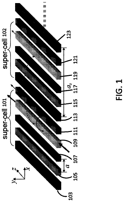
The present invention discloses a backlight module and a display device, so as to improve the luminous effect of the backlight module.
US 9,784,918 B2 · Assignee: FUJIKURA LTD. · Inventors: Oka; Akira
Sheet 1 of 18 from the published document. All sheets in the USPTO PDF
An effective refractive index of a TM0 polarized wave guided through the first core when existing alone and an effective refractive index of a TE0 polarized wave guided through the second core when existing alone are continuous as a function of a distance from a starting point of a side-by-side arrangement section. A magnitude relationship between an effective refractive index of an odd mode of a TE0 polarized wave guided through the side-by-side arrangement section and an effective refractive index of an even mode of a TM0 polarized wave guided through the side-by-side arrangement section is reversed between the starting point and an ending point of the side-by-side arrangement section. A refractive index distribution is vertically asymmetrical in an interaction section. An emission edge surface and an emission edge surface cover an entrance edge surface without excess or deficiency.
Recently, an amount of information to be transmitted over the optical communication continues to increase. In order to deal with the increased amount of information, countermeasures are taken, such as increasing a signal speed and/or increasing the number of channels employing a wavelength multiplexing communication technique. Among these, a next-generation 100 Gbps digital coherent transmission technique, which is capable of increasing a signal speed, employs a polarization multiplexing technique in order that an amount of transmittable information per unit time is doubled. According to the polarization multiplexing technique, different pieces of information are respectively carried by two types of polarized waves whose electric fields are orthogonal to each other. However, a modulation method employing the polarization multiplexing technique requires an optical modulator having a compl
1 of 18 drawing sheets so far from the published document, cropped to the drawing. Every sheet is in the USPTO PDF.
What the patent claimed, word for word. All of it is now free to use.
The present invention relates to a substrate-type optical waveguide element that serves as a polarization multiplexing waveguide. Further, the present invention also relates to an optical modulator including the substrate-type optical waveguide element.
Recently, an amount of information to be transmitted over the optical communication continues to increase. In order to deal with the increased amount of information, countermeasures are taken, such as increasing a signal speed and/or increasing the number of channels employing a wavelength multiplexing communication technique. Among these, a next-generation 100 Gbps digital coherent transmission technique, which is capable of increasing a signal speed, employs a polarization multiplexing technique in order that an amount of transmittable information per unit time is doubled. According to the polarization multiplexing technique, different pieces of information are respectively carried by two types of polarized waves whose electric fields are orthogonal to each other. However, a modulation method employing the polarization multiplexing technique requires an optical modulator having a complex structure. This results in problems such as an increase in a device size and an increase in cost.
In order to address these problems, Non-Patent Literature 1 discloses an optical modulator including a substrate-type optical waveguide that includes a core made of silicon and has advantages such as an easy manufacturing process, a smaller optical element thanks to high-density integration, and a reduction in manufacturing cost due to use of a larger-diameter wafer.
The optical modulator employing the polarization multiplexing technique includes a polarization rotator (hereinafter, abbreviated as “PR”) and a polarization beam combiner (hereinafter, abbreviated as “PBC”). FIG. 20 is a block diagram illustrating a configuration of PR 6 , whereas FIG. 21 is a block diagram illustrating a configuration of PBC 7 . PR 6 includes an input port and an output port. PR 6 receives a TE polarized wave via the input port, converts the TE polarized wave into a TM polarized wave, and outputs the TM polarized wave via the output port. PBC 7 includes a first input port, a second input port, and an output port. PBC 7 multiplexes a TE polarized wave inputted to the first input port and a TM polarized wave inputted to the second input port, and then outputs, via the output port, the TE polarized wave and the TM polarized wave thus multiplexed. By using PR 6 and PBC 7 in combination, it is possible to provide a polarization multiplexing waveguide.
FIG. 22 is a block diagram illustrating a configuration of an optical modulator 8 including a polarization multiplexing waveguide 9 . Namely, the optical modulator 8 is an optical modulator employing the polarization multiplexing technique. The optical modulator 8 includes the polarization multiplexing waveguide 9 including PR 6 and PBC 7 , a first phase modulator for modulating a TE polarized wave, and a second phase modulator for modulating a TM polarized wave.
Individual TE polarized wave light beams inputted to the respective phase modulators are modulated by independent electrical signals. Further, different pieces of information are superimposed thereon. The polarization multiplexing waveguide 9 is disposed so as to follow the phase modulators. Out of the two TE polarized waves inputted to the polarization multiplexing waveguide 9 , the TE polarized wave inputted to the first input port is converted into a TM polarized wave. Then, the TM polarized wave and the TE polarized wave inputted to the second input port are multiplexed, and a resultant of the multiplexing is outputted. Thus, by employing the polarization multiplexing waveguide, it is possible to use the first phase modulator and the second phase modulator, which have similar configurations.
Herein, the TE polarized wave refers to a mode including, as a main component, an electric field component that is in a direction (hereinafter, referred to as a “width direction” or an “x-direction”) horizontal to a substrate, in a plane perpendicular to a traveling direction of light in the substrate-type optical waveguide. Particularly, a TE polarized wave having a maximum effective refractive index is called a “TE0 polarized wave”. Meanwhile, the TM polarized wave refers to a mode including, as a main component, an electric field component that is in a direction (hereinafter, referred to as a “height direction” or a “y-direction”) perpendicular to the substrate, in the plane perpendicular to the traveling direction of light in the substrate-type optical waveguide. Particularly, a TM polarized wave having a maximum effective refractive index is called a “TM0 polarized wave”. The TE0 polarized wave and the TM0 polarized wave are confined in the waveguides strongly more than any other TE polarized waves and any other TM polarized waves. For this reason, the TE0 polarized wave and the TM0 polarized wave are waveguide modes widely used for the substrate-type optical waveguide element.
Non-Patent Literatures 2 and 3 disclose a polarized wave beam splitter. The polarized wave beam splitter disclosed by Non-Patent Literatures 2 and 3 may also serve as a polarization beam combiner when an input and an output thereof are reversed.
A substrate-type optical waveguide element according to Non-Patent Literature 2 is constituted by two elements, specifically, asymmetric Y-branching (corresponding to an asymmetric Y-junction of Non-Patent Literature 2) and a tapered waveguide having a rib waveguide structure (corresponding to a taper of Non-Patent Literature 2). In a case where the substrate-type optical waveguide element of Non-Patent Literature 2 serves as a polarization beam combiner, the asymmetric Y-branching converts, into a TE1 polarized wave, one of two TE0 polarized waves that are spatially divided, and multiplexes the TE1 polarized wave thus converted and the other one of the two TE0 polarized waves. Here, the TE1 polarized wave refers to a waveguide mode having a second maximum effective refractive index among the TE polarized waves. The tapered waveguide converts, into a TM0 polarized wave, only the TE1 polarized wave out of the TE1 polarized wave and the TE0 polarized wave multiplexed by the asymmetric Y-branching. In this manner, the element according to Non-Patent Literature 2 serves as the polarization multiplexing waveguide.
A substrate-type optical waveguide element according to Non-Patent Literature 3 is constituted by two elements, specifically, an adiabatic conversion coupler (an adiabatic coupler of Non-Patent Literature 3) and a tapered waveguide having a rib waveguide structure (a bi level taper of Non-Patent Literature 3). In a case where the substrate-type optical waveguide element of Non-Patent Literature 3 serves as a polarization beam combiner, the adiabatic conversion coupler converts, into a TE1 polarized wave, one of two TE0 polarized waves that are spatially divided, and multiplexes the TE1 polarized wave thus converted and the other one of the two TE0 polarized waves. Here, the TE1 polarized wave refers to a waveguide mode having a second maximum effective refractive index among the TE polarized waves. The tapered waveguide converts, into a TM0 polarized wave, the TE1 polarized wave out of the TE1 polarized wave and the TE0 polarized wave multiplexed by the adiabatic conversion coupler. In this manner, the element according to Non-Patent Literature 3 serves as the polarization multiplexing waveguide. CITATION LIST Non-Patent Literature
[Non-Patent Literature 1]
Po Dong, et al., “112-Gb/s Monolithic PDM-QPSK Modulator in Silicon”, ECOC2012 Th.3.B.1
[Non-Patent Literature 2] Jing Wang, et al., “Novel ultra-broadband polarization splitter-rotator based on mode-evolution tapers and a mode-sorting asymmetric Y-junction”, OPTICS EXPRESS, Vol. 22, No. 11, pp. 13565
[Non-Patent Literature 3] Wesley D. Sacher, et al., “Polarization rotator-splitters in standard active silicon photonics platforms”, OPTICS EXPRESS, Vol. 22, No. 4, pp. 3777
[Non-Patent Literature 4] Amnon Yariv, “Optical Electronics in Modern Communications (FIFTH EDITION)”, Oxford University Press
[Non-Patent Literature 5] Konrad Mertens, et al., “New Highly Efficient Polarization Converters Based on Hybrid Supermodes”, JOURNAL OF LIGHTWAVE TECHNOLOGY, Vol. 13, No. 10, pp. 2087
SUMMARY OF INVENTION Technical Problem
However, each of the substrate-type optical waveguide elements disclosed by Non-Patent Literatures 2 and 3 has the following problem. That is, a total length of the element, i.e., a device length is long, and thus it is difficult to avoid a large-size structure.
The substrate-type optical waveguide element disclosed by Non-Patent Literature 2 needs the two elements, specifically, (i) the asymmetric Y-branching for converting one TE0 polarized wave into a TE1 polarized wave and multiplexing the TE1 polarized wave and the other TE0 polarized wave and (ii) the tapered waveguide for converting the TE1 polarized wave into a TM0 polarized wave. Therefore, it is difficult to avoid a long device length.
As well as the substrate-type optical waveguide element disclosed by Non-Patent Literature 2, the substrate-type optical waveguide element disclosed by Non-Patent Literature 3 needs the two different elements in order to serve as the polarization multiplexing waveguide. Therefore, it is difficult to avoid a long device length.
An embodiment of the present invention was made in view of the above problem. An object of an embodiment of the present invention is to reduce a device length of a substrate-type optical waveguide element that serves as a polarization multiplexing waveguide, for the purpose of reducing a size of the substrate-type optical waveguide element. Solution to Problem
In order to attain the above object, a substrate-type optical waveguide element according to an embodiment of the present invention is a substrate-type optical waveguide element including: a lower cladding; a core on the lower cladding, the core including a first core and a second core arranged side by side and a third core having an entrance edge surface connected to emission edge surfaces of the first core and the second core; and an upper cladding on the lower cladding, the upper cladding covering the core, the first core and the second core being arranged side by side in a side-by-side arrangement section that is started in a starting point corresponding to entrance edge surfaces of the first core and the second core and is ended in an ending point corresponding to the emission edge surfaces of the first core and the second core, an effective refractive index of a TE0 polarized wave guided through the first core in the absence of the second core being lower than an effective refractive index of a TE0 polarized wave guided through the second core in the absence of the first core, each of the effective refractive indexes being observed in the starting point of the side-by-side arrangement section, an effective refractive index of a TM0 polarized wave guided through the first core in the absence of the second core and the effective refractive index of the TE0 polarized wave guided through the second core in the absence of the first core being continuous as a function of a distance from the starting point of the side-by-side arrangement section, a magnitude relationship between an effective refractive index of an odd mode of a TE0 polarized wave guided through the core and an effective refractive index of an even mode of a TM0 polarized wave guided through the core being reversed between the starting point and the ending point of the side-by-side arrangement section, a refractive index distribution in a cross-section of the substrate-type optical waveguide element being vertically asymmetrical, the cross-section being perpendicular to a traveling direction of light guided through the core, the cross-section being in an interaction section, in which the odd mode of the TE0 polarized wave guided through the core and the even mode of the TM0 polarized wave guided through the core interact with each other, the emission edge surface of the first core and the emission edge surface of the second core covering the entrance edge surface of the third core without excess or deficiency.
Further, the substrate-type optical waveguide element according to an embodiment of the present invention may alternatively be expressed as a substrate-type optical waveguide element including: a lower cladding; a core on the lower cladding, the core including a first core and a second core arranged side by side and a third core having an entrance edge surface connected to emission edge surfaces of the first core and the second core; and an upper cladding on the lower cladding, the upper cladding covering the core, the first core and the second core being arranged side by side in a side-by-side arrangement section that is started in a starting point corresponding to entrance edge surfaces of the first core and the second core and is ended in an ending point corresponding to the emission edge surfaces of the first core and the second core, an effective refractive index of a TE0 polarized wave guided through the first core in the absence of the second core being lower than an effective refractive index of a TE0 polarized wave guided through the second core in the absence of the first core, each of the effective refractive indexes being observed in the starting point of the side-by-side arrangement section, a magnitude relationship between an effective refractive index of an odd mode of a TE0 polarized wave guided through the core and an effective refractive index of an even mode of a TM0 polarized wave guided through the core being reversed between the starting point and the ending point of the side-by-side arrangement section, a refractive index distribution in a cross-section of the substrate-type optical waveguide element being vertically asymmetrical, the cross-section being perpendicular to a traveling direction of light guided through the core, the cross-section being in an interaction section, in which the odd mode of the TE0 polarized wave guided through the core and the even mode of the TM0 polarized wave guided through the core interact with each other, the emission edge surface of the first core and the emission edge surface of the second core covering the entrance edge surface of the third core without excess or deficiency, a mode that is the odd mode of the TE0 polarized wave in the starting point of the side-by-side arrangement section and a mode that is the even mode of the TM0 polarized wave in the starting point of the side-by-side arrangement section being continuous as a function of a distance from the starting point of the side-by-side arrangement section. Advantageous Effects of Invention
According to an embodiment of the present invention, it is possible to reduce the device length of the substrate-type optical waveguide element that serves as the polarization multiplexing waveguide.
(a) of FIG. 1 is a top view of a substrate-type optical waveguide element according to the first embodiment of the present invention. (b) through (e) of FIG. 1 are cross-sectional views of the substrate-type optical waveguide element shown in (a) of FIG. 1 .
(a) and (b) of FIG. 2 are top views of the substrate-type optical waveguide element for explaining functions of the substrate-type optical waveguide element.
(a) through (d) of FIG. 3 each show a result of numerical calculation of an electric field occurring when a TE0 polarized wave was inputted to a first entrance port of the substrate-type optical waveguide element, the numerical calculation having been performed in a respective cross-section of the substrate-type optical waveguide element, the respective cross-section being perpendicular to a traveling direction of light.
(a) through (d) of FIG. 4 each show a result of numerical calculation of an electric field occurred when a TE0 polarized wave was inputted to a second entrance port of the substrate-type optical waveguide element, the numerical calculation having been performed in a respective cross-section of the substrate-type optical waveguide element, the respective cross-section being perpendicular to the traveling direction of light.
(a) of FIG. 5 is a top view of a substrate-type optical waveguide element according to an example of the present invention. (b) through (e) of FIG. 5 are cross-sectional views of the substrate-type optical waveguide element shown in (a) of FIG. 5 .
FIG. 6 is a graph showing a result of numerical calculation of effective refractive indexes of an even mode of a TE0 polarized wave, an odd mode of a TE0 polarized wave, and an even mode of TM0 guided through a core of the substrate-type optical waveguide element according to the example of the present invention, the numerical calculation having been performed along a traveling direction of light.
(a) of FIG. 7 is a top view of a substrate-type optical waveguide element according to a comparative example of the present invention. (b) through (e) of FIG. 7 are cross-sectional views of the substrate-type optical waveguide element shown in (a) of FIG. 7 .
FIG. 8 is a graph showing a result of numerical calculation of effective refractive indexes of an even mode of a TE0 polarized wave, an odd mode of a TE0 polarized wave, and an even mode of TM0 guided through a core of the substrate-type optical waveguide element according to the comparative example of the present invention, the numerical calculation having been performed along a z-direction, which is a traveling direction of light.
FIG. 9 is a graph showing a result of numerical calculation of an electric field component in an x-direction and an electric field component in a y-direction of a waveguide mode #1 shown in FIG. 6 , the numerical calculation having performed along the z-direction, which is the traveling direction of light.
FIG. 10 is a top view of a substrate-type optical waveguide element according to a first variation of the present invention.
FIG. 11 is a top view of a substrate-type optical waveguide element according to a second variation of the present invention.
FIG. 12 is a top view of a substrate-type optical waveguide element according to an embodiment of the present invention that was used for numerical simulation.
FIG. 13 is a graph showing a result of numerical calculation of a light wavelength dependency of loss of the substrate-type optical waveguide element shown in FIG. 12 , the substrate-type optical waveguide element having a device length of 80 μm and a width W.sub.a of 400 nm.
FIG. 14 is a graph showing a result of numerical calculation of a light wavelength dependency of a polarization extinction ratio of the substrate-type optical waveguide element shown in FIG. 12 , the substrate-type optical waveguide element having a device length of 80 μm and a width W.sub.a of 400 nm.
(a) of FIG. 15 is a top view of a substrate-type optical waveguide element according to a second embodiment of the present invention. (b) through (e) of FIG. 15 are cross-sectional views of the substrate-type optical waveguide element shown in (a) of FIG. 15 .
(a) of FIG. 16 is a graph showing a result of numerical calculation of effective refractive indexes of an even mode of a TE0 polarized wave, an odd mode of a TE0 polarized wave, and an even mode of TM0 guided through a core of the substrate-type optical waveguide element according to the second embodiment of the present invention, the numerical calculation having been performed along a traveling direction of light. (b) of FIG. 16 is a graph providing an enlarged view of an interaction section i and its vicinity shown in the graph of (a) of FIG. 16 .
(a) of FIG. 17 is a top view of a substrate-type optical waveguide element according to a third embodiment of the present invention. (b) through (e) of FIG. 17 are cross-sectional views of the substrate-type optical waveguide element shown in (a) of FIG. 17 .
FIG. 18 is a graph showing a result of numerical calculation of effective refractive indexes of an even mode of a TE0 polarized wave, an odd mode of a TE0 polarized wave, and an even mode of TM0 guided through a core of the substrate-type optical waveguide element according to the third embodiment of the present invention, the numerical calculation having been performed along a traveling direction of light.
FIG. 19 is a block diagram illustrating a configuration of an optical modulator according to an application example of the present invention.
FIG. 20 is a block diagram illustrating a configuration of a known polarization rotator.
FIG. 21 is a block diagram illustrating a configuration of a known polarization beam combiner.
FIG. 22 is a block diagram illustrating a configuration of an optical modulator including the known polarization rotator and the known polarization beam combiner. DESCRIPTION OF EMBODIMENTS First Embodiment
With reference to the drawings, the following describes a first embodiment of a substrate-type optical waveguide element according to the present invention.
(Configuration of Substrate-Type Optical Waveguide Element)
With reference to FIGS. 1 and 2 , a configuration of a substrate-type optical waveguide element 1 according to the present embodiment will be described. (a) of FIG. 1 is a top view of the substrate-type optical waveguide element 1 . (b) through (e) of FIG. 1 are cross-sectional views of the substrate-type optical waveguide element 1 . (b) of FIG. 1 is an AA′ cross-sectional view taken along line A-A′ shown in (a) of FIG. 1 , (c) of FIG. 1 is a BB′ cross-sectional view taken along line B-B′ shown in (a) of FIG. 1 , (d) of FIG. 1 is a cross-sectional view of an entrance side of an ending point (z=1) of a side-by-side arrangement section I shown in (a) of FIG. 1 , and (e) of FIG. 1 is a cross-sectional view of an emission side of the ending point (z=1) of the side-by-side arrangement section I shown in (a) of FIG. 1 . The side-by-side arrangement section I will be described in detail later. (a) and (b) of FIG. 2 are top views of the substrate-type optical waveguide element 1 for explaining functions of the substrate-type optical waveguide element 1 .
As shown in (b) and (c) of FIG. 1 , the substrate-type optical waveguide element 1 includes a lower cladding 12 , a core 11 on the lower cladding 12 , and an upper cladding 13 on the lower cladding 12 , the upper cladding covering the core 11 .
As shown in (a) of FIG. 1 , the core 11 includes a first core 11 a and a second core 11 b arranged side by side, and a third core 11 c having an entrance edge surface 11 c 1 connected to an emission edge surface 11 a 2 of the first core 11 a and an emission edge surface 11 b 2 of the second core 11 b.
In the description below, a section in which the first core 11 a and the second core 11 b are arranged side by side is called the side-by-side arrangement section I. The side-by-side arrangement section I is started in a starting point corresponding to a cross-section including entrance edge surfaces 11 a 1 and 11 b 1 of the first core 11 a and the second core 11 b , and is ended in the ending point corresponding to a cross-section including the emission edge surfaces 11 a 2 and 11 b 2 of the first core 11 a and the second core 11 b . A traveling direction of light guided through the core 11 in the side-by-side arrangement section I is defined as a z-axis positive direction. A value normalized by a length of the side-by-side arrangement section I is used as a value of a coordinate z.
The entrance edge surface 11 a 1 of the first core 11 a serves as a first entrance port of the substrate-type optical waveguide element 1 . Here, a width of the first core 11 a is a width W.sub.a. Particularly, a width of the entrance edge surface 11 a 1 is a width W.sub.a1, and a width of the emission edge surface 11 a 2 is a width W.sub.a2.
The entrance edge surface 11 b of the second core 11 b serves as a second entrance port of the substrate-type optical waveguide element 1 . Here, a width of the second core 11 b is a width W.sub.b. Particularly, a width of the entrance edge surface 11 b 1 is a width W.sub.b1, and a width of the emission edge surface 11 b 2 is a width W.sub.b2.
An emission edge surface 11 c 2 of the third core 11 c serves as an emission port of the substrate-type optical waveguide element 1 . Here, a width of the third core 11 c is a width W.sub.c. In the present embodiment, the width W.sub.c of the third core 11 c is constant from the entrance edge surface 11 c 1 to the emission edge surface 11 c 2 .
The substrate-type optical waveguide element 1 is configured to satisfy the following requirements
through (5).
An effective refractive index of a TE0 polarized wave guided through the entrance edge surface 11 a 1 of the first core 11 a in the absence of the second core 11 b is lower than an effective refractive index of a TE0 polarized wave guided through the entrance edge surface 11 b 1 of the second core 11 b in the absence of the first core 11 a.
An effective refractive index of a TM0 polarized wave guided through the first core observed in the absence of the second core and the effective refractive index of the TE0 polarized wave guided through the second core observed in the absence of the first core are continuous as a function of a distance from the starting point of the side-by-side arrangement section.
A magnitude relationship between an effective refractive index of an odd mode of a TE0 polarized wave guided through the side-by-side arrangement section I and an effective refractive index of an even mode of a TM0 polarized wave guided through the side-by-side arrangement section I is reversed between the starting point and the ending point of the side-by-side arrangement section I of the core 11 .
A refractive index distribution in a cross-section of the side-by-side arrangement section I is vertically asymmetrical, the cross-section being perpendicular to a direction (z-axis direction) in which light is guided, the cross-section being in an interaction section i, in which the odd mode of the TE0 polarized wave and the even mode of the TM0 polarized wave interact with each other.
In the ending point of the side-by-side arrangement section I, the emission edge surface 11 a 2 of the first core 11 a and the emission edge surface 11 b 2 of the second core 11 b cover the entrance edge surface 11 c 1 of the third core 11 c without excess or deficiency.
In order to satisfy the requirement (1), the present embodiment defines the width W.sub.a1 of the entrance edge surface 11 a 1 of the first core 11 a and the width W.sub.b1 of the entrance edge surface 11 b 1 of the second core 11 b so that “W.sub.a1<W.sub.b1” is satisfied.
Further, in order to satisfy the requirement (2), the present embodiment employs such a configuration that cross-sectional shapes of the first core 11 a and the second core 11 b are changed continuously as the cross-sections are located closer to the ending point from the starting point in the side-by-side arrangement section I. Specifically, the present embodiment employs such a configuration that (i) heights of the first core 11 a and the second core 11 b are each set to a height h and (ii) both of the width W.sub.a and the width W.sub.b are reduced continuously as the width W.sub.a and the width W.sub.b are located closer to the ending point from the starting point in the side-by-side arrangement section I.
Further, a shape of the core 11 that satisfies the requirement
can be determined by calculation based on simulation of (i) an effective refractive index of the odd mode of the TE0 polarized wave guided through the side-by-side arrangement section I and (ii) an effective refractive index of the even mode of the TM0 polarized wave guided through the side-by-side arrangement section I.
Further, a width W.sub.a(z) of the first core 11 a in each cross-section is defined so that W.sub.a(z) becomes a continuous function having a negative slope, and a width W.sub.b(z) of the second core 11 b in each cross-section is defined so that W.sub.b(z) becomes a continuous function having a negative slope. In other words, the width W.sub.a is defined to be continuously reduced from the width W.sub.a1 to the width W.sub.a2 as the width W.sub.a is located closer to the ending point from the starting point in the side-by-side arrangement section I, and the width W.sub.b is defined to be continuously reduced from the width W.sub.b1 to the width W.sub.b2 as the width W.sub.b is located closer to the ending point from the starting point in the side-by-side arrangement section I.
Further, in order to satisfy the requirement (4), the present embodiment includes a slab 11 d , via which the first core 11 a and the second core 11 b are communicated with each other and which has a lower height than the heights of the first core 11 a and the second core 11 b.
Due to the slab 11 d provided therein, the core 11 has a vertically asymmetric cross-sectional shape. Consequently, even in a case where the lower cladding 12 and the upper cladding 13 are made of materials having an identical refractive index, a cross-section perpendicular to the direction (the z-axis direction shown in (a) of FIG. 1 ) in which light is guided has a refractive index distribution that is vertically asymmetrical. In the present embodiment, the slab 11 d is provided over the whole side-by-side arrangement section I. However, the present invention is not limited to such a configuration. Namely, the slab 11 d only needs to be provided in the interaction section i. The interaction section i will be described later with reference to another drawing.
Note that, when the requirements (1), (3), and
are satisfied, the requirement
can alternatively be expressed as a requirement (2′) below. Namely, the substrate-type optical waveguide element 1 can alternatively be expressed to be configured to satisfy the requirements (1), (2′), (3), and (4).
(2′) A mode that is the odd mode of the TE0 polarized wave in the starting point of the side-by-side arrangement section I and a mode that is the even mode of the TM0 polarized wave in the starting point of the side-by-side arrangement section I are continuous as a function of a distance from the starting point of the side-by-side arrangement section I.
As will be described later in the section “Operation Principal of Mode Conversion” with reference to FIG. 6 , a mode (#1 shown in FIG. 6 ) that is an odd mode of a TE0 polarized wave in the starting point of the side-by-side arrangement section I becomes, out of two hybrid modes, a mode having a higher effective refractive index in the interaction section i. Then, the mode becomes a mode that is an even mode of a TM0 polarized wave in the ending point of the side-by-side arrangement section I. Similarly, a mode (#2 shown in FIG. 6 ) that is an even mode of a TM0 polarized wave in the starting point of the side-by-side arrangement section I becomes, out of the two hybrid modes, a mode having a lower effective refractive index in the interaction section i. Then, the mode becomes an odd mode of a TE0 polarized wave in the ending point of the side-by-side arrangement section I.
Further, the slab 11 d brings about a side effect of strengthening optical coupling between the first core 11 a and the second core 11 b . In a configuration without the slab 11 d , most of the electric fields of light guided through the side-by-side arrangement section I are confined in the first core 11 a and the second core 11 b . Consequently, the optical coupling between the first core 11 a and the second core 11 b is not strengthened. On the other hand, in a configuration in which the core 11 includes the slab 11 d , the electric fields of light guided through the side-by-side arrangement section I greatly exude, via the slab 11 d , from the first core 11 a toward the second core 11 b and from the second core 11 b toward the first core 11 a . Consequently, the optical coupling between the first core 11 a and the second core 11 b is strengthened.
Furthermore, the slab 11 d brings about another side effect of enhancing, in the ending point of the side-by-side arrangement section I, an efficiency of entrance of light from the side-by-side arrangement section I into the third core 11 c . Note here that an even mode of a TM0 polarized wave entering the third core 11 c after being guided through the side-by-side arrangement section I can be converted into a TM0 polarized wave to be guided through the third core 11 c . Note also that, similarly, an even mode of a TE0 polarized wave entering the third core 11 c after being guided through the side-by-side arrangement section I can be converted into a TE0 polarized wave to be guided through the third core 11 c . Thanks to the slab 11 d included therein, the substrate-type optical waveguide element 1 achieves an enhanced efficiency of entrance of the even mode of the TM0 polarized wave and the even mode of the TE0 polarized wave from the side-by-side arrangement section I into the third core 11 c , so that loss is reduced. This effect is achieved thanks to the slab 11 d , which reduces discontinuity between the side-by-side arrangement section I and the third core 11 c . In other words, this effect is achieved thanks to the slab 11 d , which fills a gap between the first core 11 a and the second core 11 b in the side-by-side arrangement section I and accordingly allows cross-sectional shapes of the side-by-side arrangement section I and the third core 11 c to approximate to each other.
Moreover, in order to satisfy the requirement (5), the present embodiment is configured such that, in the ending point of the side-by-side arrangement section I, the first core 11 a and the second core 11 b are not apart from each other and the emission edge surface 11 a 2 of the first core 11 a and the emission edge surface 11 b 2 of the second core 11 b are directly in contact with each other. Further, the present embodiment is configured such that a shape of a region R 11 shown in (d) of FIG. 1 and a shape of the entrance edge surface 11 c 1 of the third core 11 c shown in (e) of FIG. 1 are congruent with each other. Here, the region R 11 is constituted by the emission edge surface 11 a 2 of the first core 11 a and the emission edge surface 11 b 2 of the second core 11 b.
Since the shape of the region R 11 and the shape of the entrance edge surface 11 c 1 are congruent with each other, the emission edge surface 11 a 2 of the first core 11 a and the emission edge surface 11 b 2 of the second core 11 b cover the entrance edge surface 11 c 1 of the third core 11 c without excess or deficiency. Namely, the substrate-type optical waveguide element 1 configured as above satisfies the requirement (5).
Note that the state where the region R 11 covers the entrance edge surface 11 c 1 without excess or deficiency herein refers to a state where the shape of the region R 11 and the shape of the entrance edge surface 11 c 1 are congruent with each other at least from a macroscopic view. Namely, if the shape of the region R 11 and the shape of the entrance edge surface 11 c 1 can be regarded as being congruent with each other from a macroscopic view even in a case where the shape of the region R 11 and the shape of the entrance edge surface 11 c 1 are not congruent with each other from a microscopic view, the region R 11 is regarded as covering the entrance edge surface 11 c 1 without excess or deficiency.
A TE0 polarized wave that has entered the first entrance port of the substrate-type optical waveguide element 1 configured as above can be regarded as an odd mode of a TE0 polarized wave to be guided through the core 11 . The odd mode of the TE0 polarized wave is converted into an even mode of a TM0 polarized wave in a process of being guided through the side-by-side arrangement section I, and then enters the third core 11 c . The even mode of the TM0 polarized wave that has entered the third core 11 c can be regarded as a TM0 polarized wave to be guided through the third core 11 c . The TM0 polarized wave guided through the third core 11 c is emitted from the emission port of the substrate-type optical waveguide element 1 (see FIG. 2 ).
Meanwhile, a TE0 polarized wave that has entered the second entrance port of the substrate-type optical waveguide element 1 can be regarded as an even mode of a TE0 polarized wave to be guided through the core 11 . The even mode of the TE0 polarized wave is guided through the side-by-side arrangement section I while maintaining its mode as the even mode of the TE0 polarized wave, and then enters the third core 11 c . The even mode of the TE0 polarized wave that has entered the third core 11 c can be regarded as a TE0 polarized wave to be guided through the third core 11 c . The TE0 polarized wave guided through the third core 11 c is emitted from the emission port of the substrate-type optical waveguide element 1 (see FIG. 2 ).
Thus, the substrate-type optical waveguide element 1 serves as a polarization multiplexing waveguide for, in a case where individual TE0 polarized waves are respectively inputted to the first entrance port and the second entrance port, (i) converting the TE0 polarized wave that has entered the first entrance port into a TM0 polarized wave and (ii) multiplexing the TM0 polarized wave thus converted and the TE0 polarized wave that has entered the second entrance port and emitting a resultant of the multiplexing. Namely, the substrate-type optical waveguide element 1 has functions of both of the polarization rotator and the polarization beam combiner, and serves as the polarization multiplexing waveguide shown in FIG. 22 .
Further, in a case where a TE0 polarized wave and a TM0 polarized wave are inputted to the emission port of the substrate-type optical waveguide element 1 , the substrate-type optical waveguide element 1 outputs a TE0 polarized wave from the first entrance port, and outputs a TE0 polarized wave from the second entrance port. Thus, the substrate-type optical waveguide element 1 has the functions of both of the polarized wave beam splitter and the polarization rotator.
Furthermore, since the substrate-type optical waveguide element 1 satisfies the requirement (5), an even mode of a TE0 polarized wave guided through the side-by-side arrangement section I and a TE0 polarized wave guided through the third core 11 c are connected to each other continuously, and an even mode of a TM0 polarized wave guided through the side-by-side arrangement section I and a TM0 polarized wave guided through the third core 11 c are connected to each other continuously. These continuous connections are always established, because the adiabatic conversion is performed such that a magnitude relationship in an effective refractive index is maintained for a single polarized wave. Specifically, a mode having a highest effective refractive index among the modes of the TE polarized wave guided through the side-by-side arrangement section I is the even mode of the TE0 polarized wave, and a mode having a highest effective refractive index among the modes of the TE polarized wave guided through the third core 11 c is the TE0 polarized wave. Therefore, the even mode of the TE0 polarized wave guided through the side-by-side arrangement section I and the TE0 polarized wave guided through the third core 11 c are connected to each other continuously. This also applies to an even mode of a TM0 polarized wave guided through the side-by-side arrangement section I and a TM0 polarized wave guided though the third core 11 c.
Therefore, the substrate-type optical waveguide element 1 that satisfies the requirement
The description continues in the full USPTO document.
About 6,747 words. The USPTO PDF has it with every drawing.
Fees are due 3.5, 7.5 and 11.5 years after grant. This patent expired on October 10, 2025, so the fee marked "not paid" was the one that went unpaid.
SUBSTRATE-TYPE OPTICAL WAVEGUIDE ELEMENT
Filed Mar 2017 · published Jun 2017Substrate-type optical waveguide element
Filed Mar 2017 · granted Oct 2017Earlier publications, parents and continuations. None of them can still be enforced, or this patent would not be listed.
Prior art cited by the examiner or applicant. Useful when you check your own idea for novelty.
Everything on this page comes from the documents linked above.