Field of the invention
The field of the present invention is light-based touch screens.
Background of the invention
Many consumer electronic devices are now being built with touch sensitive screens, for use with finger or stylus touch user inputs. These devices range from small screen devices such as mobile phones and car entertainment systems, to mid-size screen devices such as notebook computers, to large screen devices such as check-in stations at airports.
Most conventional touch screen systems are based on resistive or capacitive layers. Such systems are not versatile enough to offer an all-encompassing solution, as they are not easily scalable.
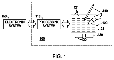
Reference is made to FIG. 1 , which is a prior art illustration of a conventional touch screen system. Such systems include an LCD display surface 606 , a resistive or capacitive overlay 801 that is placed over the LCD surface, and a controller integrated circuit (IC) 701 that connects to the overlay and converts inputs from the overlay to meaningful signals. A host device (not shown), such as a computer, receives the signals from controller IC 701 , and a device driver or such other program interprets the signals to detect a touch-based input such as a key press or scroll movement.
Reference is made to FIG. 2 , which is a prior art illustration of a conventional resistive touch screen. Shown in FIG. 2 are conductive and resistive layers 802 separated by thin spaces. A PET film 803 overlays a top circuit layer 804 , which overlays a conductive coating 806 . Similarly, a conductive coating 807 with spacer dots 808 overlays a bottom circuit layer 805 , which overlays a glass layer 607 . When a pointer 900 , such as a finger or a stylus, touches the screen, a contact is created between resistive layers, closing a switch. A controller 701 determines the current between layers to derive the position of the touch point.
Advantages of resistive touch screens are their low cost, low power consumption and stylus support.
A disadvantage of resistive touch screens is that as a result of the overlay, the screens are not fully transparent. Another disadvantage is that pressure is required for touch detection; i.e., a pointer that touches the screen without sufficient pressure goes undetected. As a consequence, resistive touch screens do not detect finger touches well. Another disadvantage is that resistive touch screens are generally unreadable in direct sunlight. Another disadvantage is that resistive touch screens are sensitive to scratches. Yet another disadvantage is that resistive touch screens are unable to discern that two or more pointers are touching the screen simultaneously, referred to as “multi-touch”.
Reference is made to FIG. 3 , which is a prior art illustration of a conventional surface capacitive touch screen. Shown in FIG. 3 is a touch surface 809 overlaying a coated glass substrate 810 . Two sides of a glass 811 are coated with a uniform conductive indium tin oxide (ITO) coating 812 . In addition, a silicon dioxide hard coating 813 is coated on the front side of one of the ITO coating layers 812 . Electrodes 814 are attached at the four corners of the glass, for generating an electric current. A pointer 900 , such as a finger or a stylus, touches the screen, and draws a small amount of current to the point of contact. A controller 701 then determines the location of the touch point based on the proportions of current passing through the four electrodes.
Advantages of surface capacitive touch screens are finger touch support and a durable surface.
A disadvantage of surface capacitive touch screens is that as a result of the overlay, the screens are not fully transparent. Another disadvantage is a limited temperature range for operation. Another disadvantage is a limited capture speed of pointer movements, due to the capacitive nature of the touch screens. Another disadvantage is that surface capacitive touch screens are susceptible to radio frequency (RF) interference and electromagnetic (EM) interference. Another disadvantage is that the accuracy of touch location determination depends on the capacitance. Another disadvantage is that surface capacitive touch screens cannot be used with gloves. Another disadvantage is that surface capacitive touch screens require a large screen border. As a consequence, surface capacitive touch screens cannot be used with small screen devices. Yet another disadvantage is that surface capacitive touch screens are unable to discern a multi-touch.
Reference is made to FIG. 4 , which is a prior art illustration of a conventional projected capacitive touch screen. Shown in FIG. 4 are etched ITO layers 815 that form multiple horizontal (x-axis) and vertical (y-axis) electrodes. Etched layers 815 include outer hard coat layers 816 and 817 , an x-axis electrode pattern 818 , a y-axis electrode pattern 819 , and an ITO glass 820 in the middle. AC signals 702 drive the electrodes on one axis, and the response through the screen loops back via the electrodes on the other axis. Location of a pointer 900 touching the screen is determined based on the signal level changes 703 between the horizontal and vertical electrodes.
Advantages of projective capacitive touch screens are finger multi-touch detection and a durable surface.
A disadvantage of projected capacitive touch screens is that as a result of the overlay, the screens are not fully transparent. Another disadvantage is their high cost. Another disadvantage is a limited temperature range for operation. Another disadvantage is a limited capture speed, due to the capacitive nature of the touch screens. Another disadvantage is a limited screen size, typically less than 5″. Another disadvantage is that surface capacitive touch screens are susceptible to RF interference and EM interference. Yet another disadvantage is that the accuracy of touch location determination depends on the capacitance.
It will thus be appreciated that conventional touch screens are not ideal for general use with small mobile devices and devices with large screens. It would thus be beneficial to provide touch screens that overcome the disadvantages of conventional resistive and capacitive touch screens described above.
Summary of the description
Aspects of the present invention provide novel controllers for light-based touch screens. In one embodiment, the present invention provides a controller that is a programmable state machine, and that executes a scanning program on a series of light emitters and light detectors. The controller supports three modes of operation; namely, a low power shutdown mode, a standby mode, and a scanning mode.
The controller does not require a processor core, such as an ARM core. As such, the cost of light-based touch screens using the controller is much less than capacitive touch screens.
There is thus provided in accordance with an embodiment of the present invention a controller for a light-based touch screen including a chip package coupled with a light-based touch screen, emitter driver circuitry inside the chip package for selectively activating a plurality of photoemitters that are outside of the chip package, detector driver circuitry inside the chip package for selectively activating a plurality of photo detectors that are outside of the chip package, detector signal processing circuitry for generating detection signals representing measured amounts of light detected on the plurality of photo detectors, a first plurality of signal conducting pins for connecting the plurality of photoemitters outside the chip package to the emitter driver circuitry inside the chip package, a second plurality of signal conducting pins for connecting the plurality of photo detectors outside the chip package to the detector driver circuitry and to the detector signal processing circuitry inside the chip package, controller circuitry inside the chip package for controlling the emitter driver circuitry and the detector driver circuitry, and at least one input/output pin for communicating with a host processor and for outputting the detection signals generated by the detector signal processing circuitry to the host processor, for the host processor to identify one or more locations on the touch screen that are being touched.
There is additionally provided in accordance with an embodiment of the present invention a touch screen system, including a housing, a display mounted on the housing, a host processor mounted in the housing, for determining touch locations on the display, a plurality of light emitters for emitting light that is transmitted over the display, a plurality of light receivers for producing output values based on detected light emitted by the emitters, and first and second controllers connected to the host processor, to the emitters and to the receivers, for receiving scan configuration settings from the host processor, for activating the emitters in a substantially uninterrupted scan sequence in accordance with the scan configuration settings, and for storing output values from the receivers, wherein the numbers of the light emitters and the light receivers are greater than the respective numbers of light emitters and light receivers supported by the signal conducting pins of each of the first and second controllers.
Brief description of the drawings
The present invention will be more fully understood and appreciated from the following detailed description, taken in conjunction with the drawings in which:
FIG. 1 is a prior art illustration of a conventional touch screen system;
FIG. 2 is a prior art illustration of a conventional resistive touch screen;
FIG. 3 is a prior art illustration of a conventional surface capacitive touch screen;
FIG. 4 is a prior art illustration of a conventional projected capacitive touch screen;
FIG. 5 is an illustration of a portion of a touch screen including a plurality of emitters that are positioned close together, wherein light is guided by fiber optic light guides to locations along a first screen edge, in accordance with an embodiment of the present invention;
FIG. 6 is a diagram of a touch screen having 16 emitters and 16 receivers, in accordance with an embodiment of the present invention;
FIGS. 7-9 are diagrams of the touch screen of FIG. 6 , showing detection of two pointers that touch the screen simultaneously, in accordance with an embodiment of the present invention;
FIGS. 10 and 11 are diagrams of a touch screen that detects a two finger glide movement, in accordance with an embodiment of the present invention;
FIG. 12 is a circuit diagram of the touch screen from FIG. 6 , in accordance with an embodiment of the present invention;
FIG. 13 is a simplified diagram of a light-based touch screen system, in accordance with an embodiment of the present invention;
FIG. 14 is a simplified cross-sectional diagram of the touch screen system of FIG. 13 , in accordance with an embodiment of the present invention;
FIG. 15 is a simplified illustration of an arrangement of emitters, receivers and optical elements that enable a touch screen system to read pointers that are smaller than the sensor elements, in accordance with an embodiment of the present invention;
FIG. 16 is a simplified illustration of an arrangement of emitters, receivers and optical elements that enable a touch screen system to detect a pointer that is smaller than the sensor elements, including inter alia a stylus, in accordance with an embodiment of the present invention;
FIG. 17 is a simplified diagram of a touch screen with wide light beams covering the screen, in accordance with an embodiment of the present invention;
FIG. 18 is a simplified illustration of a collimating lens, in accordance with an embodiment of the present invention;
FIG. 19 is a simplified illustration of a collimating lens in cooperation with a light receiver, in accordance with an embodiment of the present invention;
FIG. 20 is a simplified illustration of a collimating lens having a surface of micro-lenses facing an emitter, in accordance with an embodiment of the present invention;
FIG. 21 is a simplified illustration of a collimating lens having a surface of micro-lenses facing a receiver, in accordance with an embodiment of the present invention;
FIG. 22 is a simplified diagram of an electronic device with a wide-beam touch screen, in accordance with an embodiment of the present invention;
FIG. 23 is a diagram of the electronic device of FIG. 22 , depicting overlapping light beams from one emitter detected by two receivers, in accordance with an embodiment of the present invention;
FIG. 24 is a diagram of the electronic device of FIG. 22 , depicting overlapping light beams from two emitters detected by one receiver, in accordance with an embodiment of the present invention;
FIG. 25 is a diagram of the electronic device of FIG. 22 , showing that points on the screen are detected by at least two emitter-receiver pairs, in accordance with an embodiment of the present invention;
FIG. 26 is a simplified diagram of a wide-beam touch screen, showing an intensity distribution of a light signal, in accordance with an embodiment of the present invention;
FIG. 27 is a simplified diagram of a wide-beam touch screen, showing intensity distributions of overlapping light signals from two emitters, in accordance with an embodiment of the present invention;
FIG. 28 is a simplified diagram of a wide-beam touch screen, showing intensity distributions of two sets of overlapping light signals from one emitter, in accordance with an embodiment of the present invention;
FIG. 29 is a simplified diagram of a wide beam touch screen with emitter and receiver lenses that do not have micro-lens patterns, in accordance with an embodiment of the present invention;
FIGS. 30 and 31 are simplified diagrams of a wide-beam touch screen with emitter and receiver lenses that have micro-lens patterns, in accordance with an embodiment of the present invention;
FIG. 32 is a simplified diagram of a wide-beam touch screen with emitter and receiver lenses that do not have micro-lens patterns, in accordance with an embodiment of the present invention;
FIG. 33 is a simplified diagram of a wide beam touch screen, with emitter and receiver lenses that have micro-lens patterns, in accordance with an embodiment of the present invention;
FIG. 34 is a simplified diagram of two emitters with lenses that have micro-lens patterns integrated therein, in accordance with an embodiment of the present invention;
FIG. 35 is a simplified diagram of two receivers with lenses that have micro-lens patterns integrated therein, in accordance with an embodiment of the present invention;
FIG. 36 is a simplified diagram of a side view of a single-unit light guide, in the context of an electronic device with a display and an outer casing, in accordance with an embodiment of the present invention;
FIG. 37 is a simplified diagram of side views, from two different angles, of a lens with applied feather patterns on a surface, in accordance with an embodiment of the present invention;
FIG. 38 is a simplified diagram of a portion of a wide-beam touch screen, in accordance with an embodiment of the present invention;
FIG. 39 is a top view of a simplified diagram of light beams entering and exiting micro-lenses etched on a lens, in accordance with an embodiment of the present invention;
FIG. 40 is a simplified diagram of a side view of a dual-unit light guide, in the context of a device having a display and an outer casing, in accordance with an embodiment of the present invention;
FIG. 41 is a picture of light guide units, within the content of a device having a PCB and an outer casing, in accordance with an embodiment of the present invention;
FIG. 42 is a top view of the light guide units of FIG. 41 , in accordance with an embodiment of the present invention;
FIG. 43 is a simplified diagram of a side view cutaway of a light guide within an electronic device, in accordance with an embodiment of the present invention;
FIG. 44 is a simplified diagram of a side view cutaway of a portion of an electronic device and an upper portion of a light guide with at least two active surfaces for folding light beams, in accordance with an embodiment of the present invention;
FIG. 45 is a simplified drawing of a section of a transparent optical touch light guide, formed as an integral part of a protective glass covering a display, in accordance with an embodiment of the present invention;
FIG. 46 is a simplified illustration of the electronic device and light guide of FIG. 44 , adapted to conceal the edge of the screen, in accordance with an embodiment of the present invention;
FIG. 47 is a simplified diagram of a light guide that is a single unit extending from opposite an emitter to above a display, in accordance with an embodiment of the present invention;
FIG. 48 is a simplified diagram of a dual-unit light guide, in accordance with an embodiment of the present invention;
FIG. 49 is a simplified diagram of a touch screen device held by a user, in accordance with an embodiment of the present invention;
FIG. 50 is a simplified diagram of a touch screen with wide light beams covering the screen, in accordance with an embodiment of the present invention;
FIGS. 51-53 are respective simplified side, top and bottom views of a light guide in the context of a device, in accordance with an embodiment of the present invention;
FIG. 54 is a simplified illustration of a touch screen surrounded by emitters and receivers, in accordance with an embodiment of the present invention;
FIG. 55 is a simplified illustration of an optical element with an undulating angular pattern of reflective facets, shown from three angles, in accordance with an embodiment of the present invention;
FIG. 56 is a simplified illustration of an optical element reflecting, collimating and interleaving light from two neighboring emitters, in accordance with an embodiment of the present invention;
FIG. 57 is a simplified diagram of a multi-faceted optical element, in accordance with an embodiment of the present invention;
FIG. 58 is a simplified graph showing the effect of various reflective facet parameters on light distribution for nine facets, in accordance with an embodiment of the present invention;
FIG. 59 is a simplified illustration of a touch screen with a wide light beam crossing the screen, in accordance with an embodiment of the present invention;
FIG. 60 is a simplified illustration of a touch screen with two wide light beams crossing the screen, in accordance with an embodiment of the present invention;
FIG. 61 is a simplified illustration of a touch screen with three wide light beams crossing the screen, in accordance with an embodiment of the present invention;
FIG. 62 is a simplified graph of light distribution of a wide beam in a touch screen, in accordance with an embodiment of the present invention;
FIG. 63 is a simplified illustration of detection signals from three wide beams as a fingertip moves across a screen, in accordance with an embodiment of the present invention;
FIGS. 64-66 are simplified graphs of light distribution in overlapping wide beams in a touch screen, in accordance with an embodiment of the present invention;
FIG. 67 is a simplified graph of detection signals from a wide beam as a fingertip moves across a screen at three different locations, in accordance with an embodiment of the present invention;
FIG. 68 is a simplified diagram of four optical elements and four neighboring emitters, in accordance with an embodiment of the present invention;
FIG. 69 is a simplified diagram of a diffractive surface that directs beams from two emitters along a common path, in accordance with an embodiment of the present invention;
FIG. 70 is a simplified diagram of a touch screen surrounded with alternating emitters and receivers, in accordance with an embodiment of the present invention;
FIG. 71 is a simplified illustration of a touch screen surrounded with alternating emitters and receivers, and a wide beam crossing the screen, in accordance with an embodiment of the present invention;
FIG. 72 is a simplified illustration of a touch screen surrounded with alternating emitters and receivers and two wide beams crossing the screen, in accordance with an embodiment of the present invention;
FIG. 73 is a simplified illustration of a touch screen surrounded with alternating emitters and receivers and three wide beams crossing the screen, in accordance with an embodiment of the present invention;
FIG. 74 is a simplified illustration of a collimating optical element reflecting and interleaving light for an emitter and a neighboring receiver, in accordance with an embodiment of the present invention;
FIGS. 75-78 are illustrations of multi-touch locations that are ambiguous vis-à-vis a first orientation of light emitters, in accordance with an embodiment of the present invention;
FIGS. 79-81 are illustrations of the multi-touch locations of FIGS. 75-77 that are unambiguous vis-à-vis a second orientation of light emitters, in accordance with an embodiment of the present invention;
FIG. 82 is a simplified illustration of a touch screen with light beams directed along four axes, in accordance with an embodiment of the present invention;
FIG. 83 is a simplified illustration of an alternate configuration of light emitters and light receivers with two grid orientations, in accordance with an embodiment of the present invention;
FIG. 84 is a simplified illustration of a configuration of alternating light emitters and light receivers, in accordance with an embodiment of the present invention;
FIG. 85 is a simplified illustration of two wide light beams from an emitter being detected by two receivers, in accordance with an embodiment of the present invention;
FIG. 86 is a simplified illustration of two wide beams and an area of overlap between them, in accordance with an embodiment of the present invention;
FIG. 87 is a simplified illustration of a touch point situated at the edges of detecting light beams, in accordance with an embodiment of the present invention;
FIG. 88 is a simplified illustration of an emitter along one edge of a display screen that directs light to receivers along two edges of the display screen, in accordance with an embodiment of the present invention;
FIGS. 89 and 90 are simplified illustrations of a lens for refracting light in three directions, having a lens surface with a repetitive pattern of substantially planar two-sided and three-sided recessed cavities, respectively, in accordance with embodiments of the present invention;
FIGS. 91-93 are simplified illustrations of a touch screen surrounded with alternating emitters and receivers and diagonal wide beams crossing the screen, in accordance with an embodiment of the present invention;
FIG. 94 is a simplified graph of light distribution across a diagonal wide beam in a touch screen, in accordance with an embodiment of the present invention;
FIG. 95 is a simplified graph of light distribution across three overlapping diagonal wide beams in a touch screen, in accordance with an embodiment of the present invention;
FIG. 96 is a simplified graph of touch detection as a finger glides across three overlapping diagonal wide beams in a touch screen, in accordance with an embodiment of the present invention;
FIG. 97 is a simplified graph of detection signals from a diagonal wide beam as a fingertip moves across the screen at three different locations, in accordance with an embodiment of the present invention;
FIG. 98 is a simplified illustration of a first embodiment for a touch screen surrounded with alternating emitters and receivers, whereby diagonal and orthogonal wide beams crossing the screen are detected by one receiver, in accordance with an embodiment of the present invention;
FIG. 99 is a simplified illustration of a second embodiment for a touch screen surrounded with alternating emitters and reciters, whereby diagonal and orthogonal wide beams crossing the screen are detected by one receiver, in accordance with an embodiment of the present invention;
FIG. 100 is a simplified illustration of a user writing on a prior art touch screen with a stylus;
FIG. 101 is a simplified illustration of light beams detecting location of a stylus when a user's palm rests on a touch screen, in accordance with an embodiment of the present invention;
FIG. 102 is a simplified illustration of a frame surrounding a touch screen, in accordance with an embodiment of the present invention;
FIG. 103 is a simplified illustration of a first embodiment of emitters, receivers and optical elements for a corner of a touch screen, in accordance with an embodiment of the present invention;
FIG. 104 is a simplified illustration of a second embodiment of emitters, receivers and optical elements for a corner of a touch screen, in accordance with an embodiment of the present invention;
FIG. 105 is an illustration of optical components made of plastic material that is transparent to infrared light, in accordance with an embodiment of the present invention;
FIG. 106 is a simplified diagram of a side view of a touch screen with light guides, in accordance with an embodiment of the present invention;
FIG. 107 is an illustration of a touch screen with a block of three optical components on each side, in accordance with an embodiment of the present invention;
FIG. 108 is a magnified illustration of one of the emitter blocks of FIG. 107 , in accordance with an embodiment of the present invention;
FIG. 109 is an illustration of a touch screen having a long thin light guide along a first edge of the screen, for directing light over the screen, and having an array of light receivers arranged along an opposite edge of the screen for detecting the directed light, and for communicating detected light values to a calculating unit, in accordance with an embodiment of the present invention;
FIG. 110 is an illustration of a touch screen having an array of light emitters along a first edge of the screen for directing light beams over the screen, and having a long thin light guide for receiving the directed light beams and for further directing them to light receivers situated at both ends of the light guide, in accordance with an embodiment of the present invention;
FIG. 111 is an illustration of two light emitters, each emitter coupled to each end of a long thin light guide, in accordance with an embodiment of the present invention;
FIGS. 112-115 are illustrations of a touch screen that detects occurrence of a hard press, in accordance with an embodiment of the present invention;
FIGS. 116 and 117 are bar charts showing increase in light detected, when pressure is applied to a rigidly mounted 7-inch LCD screen, in accordance with an embodiment of the present invention;
FIG. 118 is a simplified diagram of an image sensor positioned beneath a screen glass display, to capture an image of the underside of the screen glass and touches made thereon, in accordance with an embodiment of the present invention;
FIG. 119 is a simplified diagram of a display divided into pixels, and three touch detections, in accordance with an embodiment of the present invention;
FIG. 120 is a simplified diagram of a camera sensor positioned on a hinge of a laptop computer and pointing at a screen, in accordance with an embodiment of the present invention;
FIG. 121 is a simplified side view diagram showing a camera viewing a touch area, in accordance with an embodiment of the present invention;
FIG. 122 is a simplified top view diagram showing a camera viewing a touch area, in accordance with an embodiment of the present invention;
FIG. 123 is a simplified diagram of a camera viewing a touch area, and two image axes, an image x-axis and an image y-axis, for locating a touch pointer based on an image captured by the camera, in accordance with an embodiment of the present invention;
FIG. 124 is a simplified diagram of a camera viewing a touch area, and two screen axes, a screen x-axis and a screen y-axis, for locating a touch pointed based on an image captured by the camera, in accordance with an embodiment of the present invention;
FIGS. 125 and 126 are simplified diagrams of two cameras, each capturing a touch area from different angles, in accordance with an embodiment of the present invention;
FIG. 127 is a simplified diagram of four cameras, each capturing a touch area from different angles, in accordance with an embodiment of the present invention;
FIG. 128 is a simplified diagram, from a camera viewpoint, of a camera viewing a complete touch area, in accordance with an embodiment of the present invention;
FIG. 129 is a simplified diagram of a portion of a touch area showing a stylus and a mirror image of the stylus, which are tangent to one another, in accordance with an embodiment of the present invention;
FIG. 130 is a simplified diagram showing a stylus and a mirror image of the stylus, moved closer to the center of a touch area vis-à-vis FIG. 129 , in accordance with an embodiment of the present invention;
FIG. 131 is a simplified diagram showing a stylus and a mirror image of the stylus, moved closer to the bottom of a touch area vis-à-vis FIG. 129 , in accordance with an embodiment of the present invention;
FIG. 132 is a simplified diagram showing a stylus and a mirror image of the stylus, separated apart from one another, in accordance with an embodiment of the present invention;
FIG. 133 is a simplified flowchart of a method for determining a three-dimensional pointed location, in accordance with an embodiment of the present invention;
FIG. 134 is a simplified diagram of a touch area that displays six touch icons, used for determining a camera orientation, in accordance with an embodiment of the present invention;
FIGS. 135 and 136 are illustrations of opposing rows of emitter and receiver lenses in a touch screen system, in accordance with an embodiment of the present invention;
FIG. 137 is a simplified illustration of a technique for determining a touch location, by a plurality of emitter-receiver pairs in a touch screen system, in accordance with an embodiment of the present invention;
FIG. 138 is an illustration of a light guide frame for the configuration of FIGS. 135 and 136 , in accordance with an embodiment of the present invention;
FIG. 139 is a simplified flowchart of a method for touch detection for a light-based touch screen, in accordance with an embodiment of the present invention;
FIGS. 140-142 are illustrations of a rotation gesture, whereby a user places two fingers on the screen and rotates them around an axis;
FIGS. 143-146 are illustrations of touch events at various locations on a touch screen, in accordance with an embodiment of the present invention;
FIGS. 147-150 are respective bar charts of light saturation during the touch events illustrated in FIGS. 143-146 , in accordance with an embodiment of the present invention;
FIG. 151 is a simplified flowchart of a method for determining the locations of simultaneous, diagonally opposed touches, in accordance with an embodiment of the present invention;
FIG. 152 is a simplified flowchart of a method for discriminating between clockwise and counter-clockwise gestures, in accordance with an embodiment of the present invention;
FIG. 153 is a simplified flowchart of a method of calibration and touch detection for a light-based touch screen, in accordance with an embodiment of the present invention;
FIG. 154 is a picture showing the difference between signals generated by a touch, and signals generated by a mechanical effect, in accordance with an embodiment of the present invention;
FIG. 155 is a simplified diagram of a control circuit for setting pulse strength when calibrating a light-based touch screen, in accordance with an embodiment of the present invention;
FIG. 156 is a plot of calibration pulses for pulse strengths ranging from a minimum current to a maximum current, for calibrating a light-based touch screen in accordance with an embodiment of the present invention;
FIG. 157 is a simplified pulse diagram and a corresponding output signal graph, for calibrating a light-based touch screen, in accordance with an embodiment of the present invention;
FIG. 158 is an illustration showing how a capillary effect is used to increase accuracy of positioning a component, such as an emitter or a receiver, on a printed circuit board, in accordance with an embodiment of the present invention;
FIG. 159 is an illustration showing the printed circuit board of FIG. 158 , after having passed through a heat oven, in accordance with an embodiment of the present invention;
FIG. 160 is a simplified illustration of a light-based touch screen and an ASIC controller therefor, in accordance with an embodiment of the present invention;
FIG. 161 is a circuit diagram of a chip package for a controller of a light-based touch screen, in accordance with an embodiment of the present invention;
FIG. 162 is a circuit diagram for six rows of photo emitters with 4 or 5 photo emitters in each row, for connection to the chip package of FIG. 161 , in accordance with an embodiment of the present invention;
FIG. 163 is a simplified illustration of a touch screen surrounded by emitters and receivers, in accordance with an embodiment of the present invention;
FIG. 164 is a simplified application diagram illustrating a touch screen configured with two controllers, in accordance with an embodiment of the present invention;
FIG. 165 is a graph showing performance of a scan sequence using a conventional chip vs. performance of a scan using a dedicated controller of the present invention;
FIG. 166 is a simplified illustration of a touch screen having a shift-aligned arrangement of emitters and receivers, in accordance with an embodiment of the present invention; and
FIG. 167 is a simplified diagram of a touch screen having alternating emitters and receivers along each screen edge, in accordance with an embodiment of the present invention.
For reference to the figures, the following index of elements and their numerals is provided. Elements numbered in the 100's generally relate to light beams, elements numbered in the 200's generally relate to light sources, elements numbered in the 300's generally relate to light receivers, elements numbered in the 400's and 500's generally relate to light guides, elements numbered in the 600's generally relate to displays, elements numbered in the 700's generally relate to circuit elements, elements numbered in the 800's generally relate to electronic devices, and elements numbered in the 900's generally relate to user interfaces. Elements numbered in the 1000's are operations of flow charts.
Similarly numbered elements represent elements of the same type, but they need not be identical elements.
TABLE-US-00001 Elements generally related to light beams Element Description 100-102 Light beams 105, 106 Reflected light beam 107-109 Arc of light output from light source 110 Dist between centers of two beams 111 Dist from emitter/rcvr to opt element 112 Refracted beam 113-117 Blocked light beams 142 Arc of light output from light source 143 Arc of light input to light receiver 144 Wide light beams 145-148 Edge of wide light beam 151-154 Light beams 158 Wide light beam 167-169 Wide light beam 170-172 Signals received by light receivers 173 Beam from 1 emitter to 2 receivers 174 Beam from 1 emitter to 1.sup.st receiver 175 Beam from 1 emitter to 2.sup.nd receiver 176 Beam from emitter to 1.sup.st receiver 177 Beam from emitter to 2.sup.nd receiver 178 Beam from 1 emitter to 1.sup.st receiver 179 Beam from 1 emitter to 2.sup.nd receiver 182 Beam from 1 emitter to 2 receivers 183-187 Middle of arc of light 190 Light beams output from light source 191 Light beams input to light receiver 192 Arcs of light 193 Wide light beam from two sources
TABLE-US-00002 Elements generally related to light sources Element Description 200-213 Light emitters 220 LED cavity 230 Combined emitter-receiver elements 235-241 Light emitters
TABLE-US-00003 Elements generally related to light receivers Element Description 300-319 Light receivers 394 Light receiver 398 Light receiver/light emitter
TABLE-US-00004 Elements generally related to light guides Element Description 400 Lens 401, 402 Fiber optic light guides 407 Raised reflector bezel 408 Cutout 437, 438 Reflector & lens 439-443 Lens 444 Micro-lenses 445 Surface with fan of micro-lenses 450 Light guide 451, 452 Internally reflective surface 453, 454 Light guide surface 455 Light guide 456 Internally reflective surface 457 Collimating lens & reflective surface 458 Micro-lenses 459 Light guide surface 460 Surface with fan of micro-lenses 461 Lens 462 Micro-lenses 463 Upper portion of light guide 464 Lower portion of light guide 465 Light guide surface 466 Surface with parallel row micro-lenses 467 Parallel row pattern of micro-lenses 468 Light guide 469, 470 Internally reflective surface 471 Light guide surface 472 Light guide 473 Internally reflective surface 474 Light guide surface 475 Focal line of a lens 476 Light guide 477 Internally reflective surface 478 Light guide surface 479 Light guide 480 Internally reflective surface 481 Light guide surface 482 Black plastic transmissive element 483 Light guide 484 Surface with fan of micro-lenses 485 Upper portion of light guide 486 Lower portion of light guide 487 Surface with parallel row micro-lenses 488, 489 Optical component 490-492 Surface of optical component 493 Multi-faceted reflective surface 494-497 Optical component 498, 499 Light guide 500-501 Emitter optical component block 502-503 Receiver optical component block 504 Emitter lenses 505 Receiver lenses 506, 507 Emitter optical component 508-510 Receiver optical component 511 Emitter optical components 512 Receiver optical components 513 Optical component/temporary guide 514 Long thin light guide 515 Light guide reflector 516 Micro-lenses 517 Light scatterer strip 518, 519 Light guides 520, 521 Protruding lips on light guides 522, 523 Relative position of light guide element 524 Clear, flat glass 525 Collimating lens 526 Clear flat glass with micro-lens surface 527 Lens with pattern of refracting surfaces 528 Micro-lens pattern 530-534 Opt element with multi-faceted surface 541 Optical element surface 542 Multi-faceted reflective surface 545-549 Reflective facets 550-552 Lens section in multi-lens assembly 555, 556 Air gap 559 Connector joining lens section 560 Diffractive surface
TABLE-US-00005 Elements generally related to displays Element Description 600 Screen glass 606 LCD display (prior art) 607 Screen glass (prior art) 635-637 Display 638 Protective glass 639 Daylight filter sheet 640 Protective glass 641 Daylight filter sheet 642, 643 Display 645 Reflection on display glass
TABLE-US-00006 Elements generally related to circuit elements Element Description 700 Printed circuit board 701 Controller integrated circuit (pr. art) 702 AC input signal (prior art) 703 Output signal (prior art) 720 Shift register for column activation 730 Shift register for column activation 731 Chip package 732, 733 Signal conducting pins 736 Input/output pins 737 Chip select pin 740 Emitter driver circuitry 742 Emitter pulse control circuitry 750 Detector driver circuitry 753 Detector signal processing circuitry 755 Detector current filter 756 Analog-to-digital convertor 759 Controller circuitry 760, 761 Electrical pad 762, 763 Printed circuit board 764 Guide pin 765 Solder pad 766 Component solder pad 767 Solder pads after heat oven 768, 769 Notch in optical component/guide 770 Calculating unit 771 Clip-on fastener 772 Host processor 774 Touch screen controller 775 Serial Peripheral Interface (SPI)
The description continues in the full USPTO document.
 Lapsed, fee not paid26 drawings