Statement regarding federally sponsored research or development
Not Applicable THE NAMES OF THE PARTIES TO A JOINT RESEARCH AGREEMENT
Not Applicable. INCORPORATION-BY-REFERENCE OF MATERIAL SUBMITTED ON A COMPACT DISC OR AS A TEXT FILE VIA THE OFFICE ELECTRONIC FILING SYSTEM (EFS-WEB)
1.
No compact discs
2. The only text files submitted via the EFS-WEB are those that I have filed since the filing of the Provisional Patent Application mentioned under section (b) CROSS-REFERENCE TO RELATED APPLICATIONS, and the documents submitted with the present patent application.
Statement regarding prior disclosures by the inventor or a joint inventor
Not Applicable.
Background of the invention
Field of the Invention
The country is spending a lot of money on petroleum products to generate the power needed to support our life style. In addition and as a result, we are also generating large amounts of CO2, Carbon Dioxide, using this petroleum energy source, thus contributing further towards global warming, as speculated by a lot of scientists. There is an intensive drive to get off petroleum energy sources as much as possible and to start using other/alternative sources of energy, first to reduce our dependency on foreign sources of energy and second, to reduce the carbon emissions. The purpose of this invention is to help in getting us closer to this goal.
Background Art
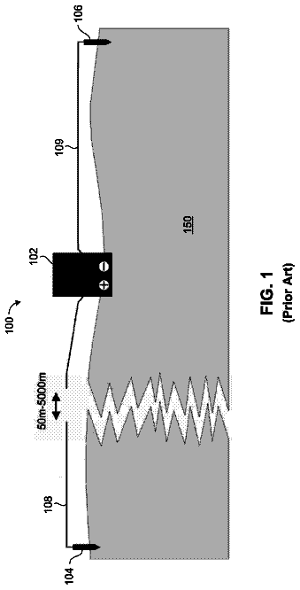
It is well known that a piezoelectric (PE) material or device can generate an electric charge or voltage and ultimately power, when it is mechanically stressed, as depicted in FIG. 1 or in FIG. 2 -A or in FIG. 5 or in FIG. 21 .
As shown in FIG. 1 , if a piezoelectric cantilever beam 101 , fixes in a support 102 is pushed down as in 103 , an electric potential can be detected at points 104 and 105 . FIG. 2 -A shows more details. Here the piezoelectric cantilever beam 201 has two electric contacts 202 and 203 near its fixation end, where it is between that clamps 204 and 205 . When the beam is pushed to positions 206 or 207 , then we can detect the electrical potential at the terminals 208 and 209 . These electrical potentials can be observed on a scope, roughly as illustrated in the graph at the left end of the FIG. 2 -A. FIG. 2 -B shows the potential, if a 4-diode, full bridge rectifier is attached between the piezoelectric beam and the scope.
And vice versa, such a PE material can move mechanically when an electrical power or charge is applied to it, as in the PE “fan” depicted in FIG. 4 . For example, there are Piezoelectric (PE) speakers, which convert electrical input signals to sound, the sound being generated by a diaphragm of some sort, which is moved mechanically by the PE element in the speaker, where the PE element has converted the electrical input signal into a mechanical movement output. The reverse is also true. There are PE lighters, which act in the reverse way. When you strike a PE element inside the lighter, by some mechanical input like pushing on the release lever, the PE element generates an electric output, which creates the spark needed to light a fire for example. This PE lighter does generate electrical power as a result of applying a mechanical input onto its PE element.
There are a certain number of materials that have/exhibit this PE phenomenon. For example, solids made out of certain ceramic materials, or sheets made out of KYNAR, usually flexible if thin enough, which is a plastic material, exhibit such a PE phenomenon.
My invention here is to utilize this PE phenomenon and such materials, to generate electric power, by applying mechanical stress and/or movements on such materials, for example from wind, from waves in the ocean or similar water bodies, or from anything that could generate a mechanical stress and/or movements in a PE material.
Of course, there should also be a way to capture the electric power that would be generated by these materials as a result of these mechanical inputs, and to store the generated electric power, or to use it or consume it right away. I propose using means to direct the generated electric power at the right instances in appropriate directions, so that if there are two units of electric power, that are generated at the same time but are of opposite polarity, then these two units would not cancel out each other. For this purpose, I am proposing a number of alternatives, described here below.
A first alternative is to use semi-conductors, such as diodes and/or transistors, to separate the output charges and collect the similar charges at individual collectors, separately from the non-similar charges, so that they do not neutralize each other. In other words, collect all the Positive (+) charges at the Positive (+) collector or terminal, and collect all the Negative (−) charges at the Negative (−) collector or terminal.
A second alternative is to break down any large size PE generator and/or Collectors into smaller units or segments. The purpose is again to reduce the chance of having one polarity charge neutralizing the opposite polarity charge, mostly by separating the generating elements from each other as much as possible and/or by separating the collectors as well, for the same purpose. All these alternatives include at the same time, features to facilitate the manufacturing processes to create the various proposed embodiments.
Further background art
I propose that we could use either a “Bridge-” like electric circuit, as in FIG. 2 -B, using “Diodes-” or “Transistors-” like devices, to capture the “instantaneous” electricity generated during the various stages of the imparted mechanical inputs. The danger is that if two adjacent PE elements are stressed or moved in opposite directions at the same time, and the electric power elements or charges generated by them are in opposite directions but are “electrically” connected, then these two charges would cancel each other out and would neutralize any usable output. So, we must find a way to separate these charges from each other and capture the benefits of each of them separately and then “add” any similar charges appropriately together, to get the benefit of applying the mechanical inputs to the PE element(s).
Most mechanical inputs can be evaluated as either producing a compression force or stress, or a tension force or stress, being applied on to the PE element. These forces or stresses can be constant or continuous, i.e. steady or hardly changing, or they can be changing either in a repeated fashion, e.g. like a wave form, or can be just individual impulses at a steady repeating manner or at some irregular intervals. Even if the applied forces or stresses create a bending situation, the end effect can still be presented or broken down as either compression or tension on the PE elements. In any case, the generated electric power should be captured instantaneously, so that one part of the generated power or charges would not negate or cancel out any of the other parts of the generated power or charges.
Let's say that in the set-up shown in FIG. 2 -A, that if we apply a downward push on the free end or tip of the cantilever, such that this downward push would generate a negative charge at the terminals at the fixed end of the cantilever, then an upward pull would generate a positive charge at the same terminals. And let's say that we keep applying these push and pull actions repeatedly. Then by using the four-element bridge as in FIG. 2 -B, we would convert all the pulses in one direction and the electric power can then be stored in a storage device, like a battery cell for example.
To maximize the utilization of the phenomena, we would like to capture the electricity generated “locally” along any spot/surface of the material, so that we don't negate a positive charge coming from one spot/surface by a negative charge coming from an adjacent spot/surface of the material, as in FIG. 3 . So, we prepare the Kynar strip with layers of “semi-conductor” material feeding the charges in one direction only to the “full conductive” longitudinal conductor, as shown, for example, in FIG. 34 , which will be described in due time later down below.
Kynar is one of the plastic materials that exhibit PE Effect (PEE). We should be able to tap this phenomenon to generate electric power. Any other material that exhibit similar PE phenomenon can be used as well.
At a trade show, a company was exhibiting a “FAN”, made more or less a shown in FIG. 4 . An electrical power was applied at the two terminals, which were attached to one fixed end of a strip of Kynar, as shown. When the A/C power was applied, the free end of the strip started to move up and down, thus moving the air in its vicinity, and acting somewhat like a fan, an air moving fan.
Well, I am proposing to do exactly the opposite or the reverse of this fan.
It is known that Piezo Electric Effect or PEE is reversible. That means that if you apply an electric signal to a PE element, you get a mechanical movement, and on the other hand, if you apply a reverse mechanical movement, e.g. by applying a force to the PE element, you get a reverse action, i.e. we get an electric signal output (power). (See FIG. 21 ).
I propose to do just that. The reverse action.
In FIG. 5 , if I hold the free tip of the (PE) Kynar strip and push it up and down with my fingers, then the theory says that the strip, being made of a Piezo Electric material, would generate an electrical voltage at the terminals. If I push the strip upwards, the voltage will have one polarity, and when I reverse and push the strip downwards, the voltage will also reverse and will have the opposite polarity.
This can be demonstrated, if such a strip with electrodes/terminals as shown is wired to a voltmeter or an oscilloscope. Then if the strip is tapped by finger or by a pencil or the like, then the signal on the scope would show an oscillation, almost like an AC electrical current signal, but the magnitude of the signal would decrease as the mechanical vibration of the strip fades away until the mechanical vibration or motion stops totally, at which time the electrical signal on the scope would stop as well.
So what I propose is to take advantage of this phenomenon to generate electricity and electrical power.
I would use such materials, any material that exhibits the PE Effect, and expose it to any means that will move it in a way that it will generate the “reverse” electrical output, and then use that output, as an electric power generated from the PE element. Lately, this kind of action is frequently referred to as “ENERGY HARVESTING”.
One of the possible moving/movement sources is “WIND”. If I use the Kynar strip or sheet as a “FLAG” and hold it in the wind, it will flutter and move hack and forth. See FIGS. 3, 6, 7, 27 , etc. I can then provide electrodes on this Kynar sheet, such that the electrical output from it can be tapped out and used as electric power in any of the various applications of electrical power. The movement of a flag in the wind is not very uniform and the electricity generated by it would also not be very uniform. But it still is electric power. If we convert it to some other useful form of electricity or power, or harness it by some clever ways, and then use it as needed, then it will be more convenient to use.
We could convert it to DC, by some kind of “RECTIFYING” processes, for example, by using DIODES, whether a single diode, or a pair of diodes or by a “4-diode bridge”, see FIGS. 2 -B, 29 , etc., or the like. We could also store this rectified power in batteries or any appropriate storage devices, e.g. capacitors, and then use that power, tapping it from these batteries, as needed and when needed. If we prefer, then we can “convert” or “invert” the DC power to an AC power, as needed.
Now let's look again at the PE Effect of a strip of Kynar. Let's go back to FIG. 5 , and let us compare that movement or deformation of the strip against the deformation of a flag, which is illustrated in FIGS. 6 and 7 .
In FIG. 5 , when we push downwards on the strip, all the fibers at the upper layers of the strip are stressed under tension, and all the fibers in the lower layers of the strip are stressed under compression. Thus if we assume that the compression stress creates NEGATIVE charges, then all the lower layers will create NEGATIVE charges. And conversely in this case, all the upper layers under the opposite kind of stress, namely tension, will create the opposite kind of charges, namely POSITIVE charges. What I am saying here is that, compression creates (−), (N) and tension creates (+), (P) charges. This may not be the exact polarity of the charges generated in true life, but be it as it may, it is the convention that I will continue using in my present specification. Just to be consistent. So, if I push down, as in Condition A in this FIG. 5 , all the positive charges will go to the UPPER terminal, while all the negative charges will go to the LOWER terminal. In this configuration, no one charge from one side of the strip will negate any charges at the opposite side of the strip.
Now let's analyze what happens in the flag shown in FIGS. 6 and 7 , using the same convention mentioned above. FIG. 7 represents the material of the flag, shown in FIG. 6 . If we assume that the deformation at point “A”, in FIG. 7 , will give us a positive (+) charge at the top/upper side of the material and a negative (−) charge at the bottom/lower side of the sheet, then the deformation at point “B” will give us charges of opposite signs at the corresponding sides of the sheet. In other words, at point B, we would get (−) charges at the top of the sheet and (+) charges at the bottom of the sheet. If these two charges travel along the surface of the sheet and we try to collect them at the terminals at points T 1 and T 2 and assuming that they will both arrive there at roughly the same time, in reality, maybe at a fraction of a second one after the other, then they will cancel each other out, and we will end up with ZERO charge at the Terminals T 1 and T 2 .
Also, the charge at the mid-point between points A and B will be ZERO, because we would have zero deformation at that point.
If we look at the timing of these two charges, we can assume that the (+) charge at A will reach the terminal point T 1 first, and a short time later, the (−) charge from point B will arrive to the terminal point T 1 and will cancel out the (+) charge that came earlier from point A and the end result is that there will be no useable charge at terminal point T 1 anymore.
So, at the top terminal T 1 , the positive charges generated at the top layers at A will be cancelled out by the negative charges generated at the top layers at B. So, there will be no residual charge accumulated, hence no power, at the top terminal T 1 . Similarly, at the bottom terminal T 2 , the negative charges generated at the bottom layers at A will be cancelled out by the positive charges generated at the bottom layers at B. So again, there will be no residual charge accumulated at T 2 , hence no power, at the bottom terminal T 2 either. So, we will end up practically with zero charge at both terminals ‘T 1 ’ and “T 2 ”. Any other charges that may be generated at other points, such as point “C” or “D” in FIG. 7 will again have the same fate and ultimately there will still be hardly any residual power for us to use. So, we would end up with practically ZERO charge and ZERO power at the terminals “T 1 ” and “T 2 ”.
So, to overcome this problem and to end up with any useful power, we need to have a clever way to separate these charges and to collect all the (+) ones together and bring them to the (+) terminal, and to collect all the (−) charges together and bring them to the (−) terminal. And we should prevent them from prematurely cancelling each other out. If we do that, then the magnitude of the charge will be considerably larger and we would have something more substantial, useful, useable output, because the charges would not have cancelled out each other, i.e. would not have neutralized themselves, as in the previous/above case, when we allowed them to intermingle.
How do we do this? Here it is further down below. This is the key/novel point of this invention.
But let us first take a brief excursion into the electronics behavior of Diodes and Transistors.
FIG. 8 shows a standard diode, wired to be in a “FORWARD BIASING” condition. Current will flow from the “p” side to the “n” side of the diode. We will use the “conventional” flow direction, not the “electron” flow direction. The “p” and the “n” sides of the diode are “doped” with certain appropriate dopants to impart to them the proper “p” and “n” characteristics, as already known in the prior art of manufacturing diodes.
This can be represented schematically as shown in FIG. 9 , showing the “Forward Bias” condition.
FIG. 10 on the other hand shows the “REVERSE BIAS” condition, since we have reversed the polarity of the battery cell or the power source, as seen in the figure. In this case, NO current flows through the circuit, because the diode does not allow any current to flow through it in this reverse bias condition. Of course if the voltage exceeds a certain limit, then the diode will break down. This danger has to be kept in mind, so as not to overload and burn the diodes. The diode size and characteristics have to be designed and selected properly. Again, all this is already known in the “prior art”.
Next, let's look at the rectifier circuits in FIGS. 11 -A and 11 -B and FIGS. 12 -A and 12 -B FIGS. 11 -A and 11 -B show a half-wave rectifier, while FIGS. 12 -A and 12 -B show a full-wave rectifier. Both have in common, the fact that the source voltage is alternating from (+) to (−) and back, while the output is all in the same one direction. Again, all this is already known in the Prior Art.
Next, I will show how we can arrive to something comparable.
Definitions and abbreviations
More definitions may appear throughout the specification text, when appropriate. (N) or (n) or (−) Negatively doped semi-conductor material (P) or (p) or (+) Positively doped semi-conductor material 1 T Conductor 2 B Conductor ABE Bus Bar (−) ABS Bus Bar (−) AC Alternative Current ATE Bus Bar Out ATS Bus Bar IN BBE Bus Bar (+) BBS Bus Bar (−) BD 1 , 2 , 3 , 4 Bottom diodes 1 , 2 , 3 and 4 . BPE Bottom Piezo-Electric Element BTE Bus Bar IN BTS Bus Bar IN C Compressive force C D 1 Diode D 2 Diode D 3 Diode D 4 Diode E 2 L Energy to the Left E 2 R Energy to the Right EP Electric Power. F-DN Flapper in the Downward position F-UP Flapper in the Upward position FHRZL Flapper in the Horizontal position Full Conductor An electrically conductive material, which conducts electricity in any direction, regardless of the polarity of the electricity. Copper is a good example. LB Level Branch, e.g. First Level Branch, Second Level Branch, etc. MO Module Outline One-Way Valve An electric circuit that allows the flow of the electric current in only one direction, similar to a one-way valve used in hydraulic applications. PE Piezoelectric PE material A material that exhibits the PE phenomenon PEE PE Effect or PE Element, depending on the text content. PEEP Piezo Electric Effect Power PES Piezo Electric Sheet Semi-Conductor A material that conducts electricity in one direction only T Tensile forces or stresses T 1 , T 2 Terminals TD 1 , 2 , 3 , 4 Top Diodes # 1 , 2 , 3 and 4 TPE Top Piezo-Electric Element W Load, electric wrt with respect to BRIEF DESCRIPTION OF THE DRAWINGS
TABLE-US-00001 FIG. # The Figure shows: 1 Cantilever piezo beam generates Electric Power 2-A Same, plus Sinusoidal Positive and Negative Output 2-B Same, plus 4-diode bridge rectifier and All Positive Output 3 Waving Flag generates positive and negative charges on its surfaces 4 Piezo Electric Fan 5 The reverse of the Fan. 6 Waving flag on a pole and its hills and valleys 7 The electric charges on the waving flag surfaces 8 Current flow in a Forward Biased Semiconductor 9 Current flow in a Forward Bias Diode 10 No current flow in a Reverse Bias Diode 11-A and Half Wave Rectifier 11-B 12-A and Full Wave Rectifier 12-B 13-A Half Wave PE generating element - Physical Schematic 13-B Flat Half Wave PE generating element - 3D View 13-C Circular Half Wave PE generating element - 3D View 14-A Full Wave PE generating element - Physical Schematic 14-B Flat Full Wave PE generating element - 3D View 15 Cable-Like Full Wave PE generating element - 3D View 16 Flex Center Conductor in a Flat Full Wave PE generating element - 3D View 17 Rollers to create Transverse Cracks 18 Rollers to create Longitudinal Cracks 19 Various PE generating gadgets, nets, tie-downs, supports, etc 20 More PE generating gadgets, nets, tie-downs, supports, etc 21 Piezo Electric crystal, with Input and Output 22 Piezo Electric Road Sensing & Energy Harvesting Element 23 Piezo Electric Road Energy Harvesting System 24 Portable Piezo Electric Corrugated Road Energy Harvesting System 25 Converting Tension to Compression 26-A, Converting Tension to Shear, or Compression or Bending 26-B, and 26-C 27 Almost Similar to FIGS. 3, 6 and 7, but detailing the individual charge sources and the resulting energy flows. 28 PEEP TREE, overview, general scheme 29 4-DIODE BRIDGE RECTIFIER, almost Similar to FIG. 2-B. 30-A Almost Similar to FIG. 29, except that the input is a PEEP Leaf. Also the output wiring is at 90 degrees wrt to the direction of the Leaf wiring. 30-B Almost Similar to FIG. 30-A, except that the output wiring is shown in line with or parallel to the PEEP Leaf wiring. 31 PEEP LEAF Basic Module with the major basic components or parts. 32-A Schematic Flow Diagram of the arrangement shown in FIG. 30-A, when the Generated Charge is Positive and Flowing Upwards as shown. 32-B Physical Cross-Section of the arrangement in FIG. 32-A, showing the physical components of the arrangement, and the current flows through the components. Again, this is for the case when the generated charge is Positive and flowing upwards as shown in FIG. 32-A. 33-A Schematic Flow Diagram in the arrangement shown in FIG. similar to the one shown in FIG. 32-A, but when the Generated Charge is Negative and Flowing Downwards as shown here. 33-B Physical Cross-Section of the arrangement in FIG. 33-A, showing the physical components of the arrangement, and the current flows through the components. This is for the case when the generated charge is Negative and flowing downwards as shown in FIG. 33-A. 34 3D view of the basic PEEP Module, Active Flag 35 Basic PEEP LEAF, with 2 Diodes, to act as One-Way Valves, and 1 Capacitor 36 Basic PEEP LEAF, connected to a storage battery, with several One-Way Valves and Capacitors 37 First Level PEEP Branch with 5 Leaves, Connected to a storage device, with one-way valves and capacitors 38 Two First Level PEEP Branches with 5 Leaves each, one at top and one at bottom of the storage device. 39 Five First Level PEEP Branches with 5 Leaves each, all at the top of the storage device, and connected to the storage device by a Second Level Branch. 40 As in FIG. 39, but duplicated at the bottom like at the top of the storage device, and again connected to the storage device by a Second Level Branch. 41 Similar to FIG. 40, but physically looks slightly different, i.e. both at the top of the storage device, although electrically identical to FIG. 40 42 Three groups of First and Second Level Branches, all three of them feeding into the same storage device. 43 Combination 2: Passive Flag, and some details of the components. 44-A Combination 2-A: Passive Flag, with Fixed End 44-B Combination 2-B: Passive Flag. with twisting End 45-A Combination 2-A, Cantilever PEEP Beam, showing its possible range of motion. 45-B Combination 2-A, Cantilever PEEP Beam UP, showing the resulting direction of energy flow. 45-C Combination 2-A, Cantilever PEEP Beam DOWN, again showing the resulting reverse direction of energy flow. Reverse direction compared to FIG. 45-B. 45-D Exploded view of Combination 2-A, showing the nomenclature of the individual parts 45-E Internal forces/stresses, exerted by the flapper on the PE elements, and the resulting Energy Flow, when the flapper is in the Upward position. 45-F Same as in FIG. 45-E, but when the flapper is in the Downward position. 46-A Combination 2-B, Top view, showing the TWISTING PEE setup. 46-B Combination 2-B, Front View of the setup shown in FIG. 46-A. 46-C Combination 2-B, Cross-Sectional Side View, when the Flapper is Up 46-D Combination 2-B, Cross-Sectional Side View, when the Flapper is Horizontal, Central position. 46-E Combination 2-B, Cross-Sectional Side View, when the Flapper is Down 46-F, Combination 2-B, Same as FIGS. 46-C, -D, and -E, but in 46-G 3D views. and 46-H 47-A, 3D views of the TWISTING PEEP Element of FIG. 46, 47-B as seen from one viewpoint. and 47-C 48-A, Same as 47-A, 47-B and 47-C, but from a different viewpoint. 48-B and 48-C 49 Bifurcated flag to increase vibration or flutter, several different views. 50 Many PEEP Leaves, constructed out of one PE Sheet, showing the details and nomenclature of the various parts 51-A, Same as FIG. 50, but showing a quasi exploded views, 51-B illustrating a method of constructing same. and 51-C 52 PEEP Leaves on a Carrying Frame Structure, general view. 53 Close-up view of a part of FIG. 52 54-A Construction of a PEEP harvester, in the shape of a Cable. 54-B Similar construction of a PEEP harvester, but in a flat configuration DETAILED DESCRIPTION OF THE INVENTION
Embodiments Group #1—Using Rectifier Circuits with PE rods, strips or sheets. Embodiment
FIG. 13 -A show the basic raw arrangement of the raw concepts, arranged in series, to simulate the arrangement shown in FIG. 11 -A. FIG. 13 -B shows a more manufacturable arrangement, to accomplish the same end purpose and goal.
Please note the reference numbers of the various components in these two figures. They end up with similar last digit for any component that has a similar function. For example, the reference number of the PEE in FIG. 13 -A end up with xxx2, and the comparable PEE in FIG. 13 -B ends up with xxx2 as well. I will try to follow this approach for as long as possibly practical to do so.
FIG. 13 shows two
embodiments according to this invention, FIGS. 13 -A, 13 -B and 13 -C, which result in an “electrical” configuration comparable to the circuit shown in FIG. 11 -A hence giving a HALF-WAVE output shown in FIG. 11 -B The PEE material 1312 or 1332 has the conducting terminal 1311 or 1331 on one side, namely the Left Hand Side (LHS) in this figure, and the p-n semi-conductor 1313 , 1314 or 1333 , 1334 on the other side, namely the Right Hand Side (RHS) in this figure, which then has another full conductor 1315 or 1335 on the farther side RHS beyond. So, the currents will flow from the PEE material 1312 or 1332 to the p-n material 1313 , 1314 or 1333 , 1334 and then to the surrounding full conductors 1315 or 1335 and 1311 or 1331 , and through the load 1316 or 1336 , but not in the reverse direction. Hence, Half-Wave flow condition. The same applies to both configurations, i.e. the flat “sheet” configuration, FIG. B, as well as the round “cable” configuration, FIG. C.
NOTE: FIG. 13 -C shows the cable configuration. In order to avoid too much clutter in the drawing, I am showing only the last digit of the reference characters of the various components. For example, reference character 1 in FIG. 13 -C correlates with items 1311 or 1331 in FIGS. 13 -A and 13 -B. Similarly, reference character 2 FIG. 13 -C correlates with 1312 and 1332 in FIGS. 13 -A and 13 -B, etc.
I have shown the rest of the correlations in the following table.
Similarly, with FIG. 15 , as will be seen further down below. The same following table shows also the correlations between the reference characters of FIG. 15 with respect to those in FIGS. 14 -A and 14 -B.
TABLE-US-00002 EQUIVALENT ABBREVIATED EQUIVALENT PARTS FOR REFERENCE PARTS FOR FIG. 13-C CHARACTER FIG. 15 1311, 1331 1 1312, 1332 2 14312, 1432R, 1432L 1313, 1333 3 1413, 1433 1314, 1334 4 1414, 1434 1315, 1335 5 1415, 1435 1316, 1336 6 1416, 1436 7 1417, 1437 8 1418, 1438 9 1419, 1439 11 1411, 1411 Embodiment
FIGS. 14 -A and 14 -B show an embodiment which result in an “electrical” configuration comparable to the FULL-WAVE output configuration, shown in FIGS. 12 -A and 12 -B. We can easily visualize that the right hand side half of the flat sheet, including the centre conductor, is similar to the flat sheet configuration shown in FIGS. 13 -A and 13 -B. The current will flow from the centre conductor 1411 or 1431 to the “right” outermost conductor 1415 or 1435 , i.e. in a left to right direction, i.e. from the PEE material, 1412 in FIG. 14 -A, or 1432 R in FIG. 14 -B, to the doped semi-conductor 1414 or 1434 , to the doped semi-conductor 1415 or 1435 , to the right full conductor 1415 or 1435 , and finally to the Load 1416 or 1436 . Now, if we add to the left of this, a similar composite structure, but in a “mirror image” configuration, except that the p-n semi-conductor 1417 , 1418 or 1437 , 1438 will be in the same direction as the p-n semi-conductor 1413 , 1414 or 1433 , 1434 in the right hand half, then the current could flow again from left to right, whenever the stresses dictate this flow direction, i.e. the current now would flow from the “left” outermost conductor 1419 or 1439 to the centre conductor 1411 or 1431 . Hence, Full-Wave rectification. This will be electrically comparable and equivalent to the condition shown in FIG. 12 -A. Note that in FIG. 14 -B, I have split the PEE in two separate parts, the first part 1432 R is on the right hand side of the common conductor 1431 , and the second part 1432 L is on the left hand side of the common conductor 1431 . Embodiment
FIG. 15 provides an embodiment that looks like a “TV CABLE” or “FLAT WIRE”, similar to the well known “TV CABLE”, which could have the well-known “dog bone” cross-section. This embodiment is the “cable version” counterpart of the FLAT SHEET version shown in FIG. 14 and provides a “FULL WAVE” output configuration as well. The lower figure, below the cable, is a duplicate of FIG. 14 -A.
In all the above figures, as well as the other figures in this specification, the cross-sectional area of the conductors and other components should be calculated and designed to accommodate the expected current flows. This is standard prior art practice. Embodiment
FIG. 16 shows one way to impart more “FLEXIBILITY” to the embodiment shown in FIG. 14 . The centre conductor 1631 is shown to be made like an expanded sheet metal, to make it easier to flex, bend, stretch or contract.
A similar approach can be used to increase the flexibility of any of the other layers shown in the above constructions. However, there should be at least one layer or component, which will be kept in a shape, that will ensure the strength and integrity of the device, so that it would not fail or break down and fall apart, if exposed to high forces exerted on the device. This could be referred to as the “back-bone” of the whole structure. This hack-bone element can be made of a high strength material and could be located at one side of the cross-section and of course would extend through the whole length of the device. It could also be made out of what is known as Super Elastic material. This applies especially to the embodiments in the shape of cables or ropes to hold down posts and the like. See further down below. See for example, FIGS. 13 -C, 15 and 52 .
Note that the semi-conductors 1633 , 1634 and 1637 , 1638 and the other components, i.e. the PEE 1632 , the full conductors 1635 and 1639 , in all the above can preferably be made of a continuous material for ease of manufacturing. For example, they can be in the shape of continuous sheets which would be laminated together, say in a hatch mode or a continuous, reel to reel process.
In some cases, certain number of these layers can be either vapor deposited, extruded, laminated, etc., one on top of the other. All these methods are well known in the prior art.
Another or an additional way to allow us to capture individual electrical charges, is to break the structure of the conductors, and especially the semi-conductor layers, into smaller segments, so that each individual segment would capture/harvest the individual charges generated by the smaller areas of the PE element or the PE sheet adjacent to them. In order to achieve this purpose, I propose a number of alternatives: One alternative is shown in FIG. 17 . A second alternative is shown in FIG. 18 . A third alternative would be a “combination of both alternative two and three together, let's say in tandem. Other alternatives include individual discrete semi-conductors mounted/disposed on the flexible Kynar and any other flexible electronics materials. Alternative One: As is shown in FIG. 17 . Here we could run the composite structure, as shown in FIGS. 13 -B, 13 -C, 14 -B, 15 and 16 , across and between a set of rollers as in FIG. 17 , so that the deposited or applied layers of semi-conductors would break into smaller segments, mostly in a direction parallel to the axis of the rollers. These could be cracks or indentations, so as to create some separations in the semi-conductor material to at least create strips or sections or islands of semi-conductor material.
We would refer to these as “Transverse” cracks. We would run some experiments to determine and select the optimum sizes/diameters of the rollers, the spacing between the rollers, and the relational position of the rollers with respect to each other, both in the vertical and the horizontal direction and to see the effect on these selections on the segment size of the semi-conductors. The selection would also be dependent on the characteristics of the semi-conductor material, e.g. its rigidity, brittleness, thickness, dryness, etc. In other words, we will try to break or at least crack the layers of p-n diode material, to create smaller, isolates “islands” and preferably at least electrically separate them from each other, so that they would conduct only in one direction, normal to the surface of the sheet, but not from one island to the other islands adjacent to it.
Alternative Two: As is shown in FIG. 18 . Here, we try to crack the deposited or applied layer(s) of P-N diode, in the “Longitudinal” direction.
Alternative Three: We would run the sheets both as in Alternative One above as well as in Alternative Two above, to ensure that we get even smaller islands, which would be cracked and/or separated both in the “Transverse” as well as in the “Longitudinal” directions. Embodiments Group #3—Using Flat Sheets, Across the Wind
FIGS. 19 and 20 show two things. One, the PE material composite sheet 1912 is in the shape of a sheet hung or spread in a direction, at some angle or ideally perpendicular to the direction of the wind or fluid 1911 that will try to move or shake the sheet. The sheet will have a similar construction or cross section as in FIG. 13 -B, 14 -B or 16 . It is mounted say between two vertical posts, in the path of the wind. If the wind moves the sheet, it will stress the sheet and create some stresses in it, in the direction of the arrows 1913 , then the PE elements, built in the sheet, will be activated, and will generate the expected electricity, which will then be rectified as explained above, and the resultant DC current/power will be diverted to an appropriate storage device or used immediately for any proper usage, e.g. to heat water, or to light an electric bulb or the like.
Another possibility is to use cables, 1917 , with similar construction or cross section as in FIG. 13 -C or 15 . When the sheet 1912 is shaken by the wind, it will be stressed in the direction of the arrows 1913 , which will induce the posts to be shaken in the direction of the arrows 1914 , thus the cable 1917 will be shaken and stressed in the direction of the arrows 1915 , thus the cables 1917 would be generating some desirable energy. The whole idea is to get the wind to “shake” the sheet and create the resulting electric power. We could create some “apertures” 1916 in the sheet, to increase the turbulence of the wind going through, thus creating more vibrations in the (sheet) material 1912 and consequently more electricity. We can have “box” shapes, like the “box kites” or similar shapes with contraption that could “multiply” the shaking effect of the wind, thus multiplying the amount of generated power. Such kite constructions are also known in the prior art.
Embodiments Group #4—Using individual PE elements, along the “Tie-Down” cables, holding a structure across the wind force or the like.
FIG. 20 shows some additional features that can be incorporated in the arrangement shown in FIG. 19 , or can be used independently.
In FIG. 2 , we see a tie-down cable 1923 holding/supporting the vertical post, which in turn is holding the flapping cloth or flag 1921 . This tie-down cable is shown pulling the post toward the left hand side of the figure. This tie-down cable can be instrumented so as to have one or more PE Element in line or in tandem with the cable as shown in FIG. 20 . An example of a PE Element 1924 here is a PE Element that can be activated under compression, e.g. a ceramic kind of PE element.
Another such a PE element is shown in FIG. 20 , to the right side of the post. It is part #1925. It is shown, being located between the post 1922 and a wall 1926 , which is on the farther right side of the figure. Again the PE element in this case is being activated under compression. This approach can be used also with any structure exposed to such movements. Examples include tall buildings, skyscrapers, trees, as well as the 2 posts in FIG. 19 , which are moved as per arrows 1914 , and the like. Also floats on top of bodies of water, where the float would be equivalent to the moving post 1922 and the fixed anchor say at the bottom of the sea would be equivalent to 1926 .
FIG. 21 just shows the basic principle of PE Elements being under a compression load F, which then created an electric potential, E, between the two ends of the PE element. Embodiment—Power from Roads
FIGS. 22 and 23 illustrate another embodiment. They show how we can generate electric power as a result of cars driving over a road pavement, which has been provided with Piezo Electric material.
FIG. 22 shows the sensor, or rather the energy harvester, and its major components, while FIG. 23 shows the general usage setup.
Here, in FIG. 23 , we show a stretch 2102 of a road, which has been instrumented as per present invention. When a vehicle 2101 drives on such a road, and hits the PEEs 2103 , the PEEs will generate an electric power, which could be transferred through proper conductors and diodes 2104 and the like, to a load 2105 . The generated electric power can then be either stored in battery cells or capacitors, or can be utilized right away, say to turn on a blinking traffic light ahead of the vehicle, at an upcoming traffic intersection or the like.
FIG. 24 shows a way to create a corrugated surface 2106 , 2107 , which can be placed at certain location of a road, and which can be utilized to generate electricity at the same time.
For example, we have an intersection near where I live, where the road approaching the intersection has been provided with grooves 2107 across the road, to create vibrations in the car and in turn to alert the drivers of the approaching intersection. There are 4 or 5 groups of such grooves, placed at various distances between each grove and between each group of grooves.
These grooves have been carved out of the pavement. The pavement can be made of concrete or asphalt, and carving out these grooves can be difficult and costly.
The description continues in the full USPTO document.
 Lapsed, fee not paid6 drawings

