Lapsed, fee not paid5 drawings
Hardware & Electronics · US 9,760,481 B2
Multiport memory
A data storage device includes a memory that has a three-dimensional (3D) memory configuration, a controller, and a plurality of memory ports.
US 9,760,747 B2 · Assignee: CANON KABUSHIKI KAISHA · Inventors: Kaechi; Shuya
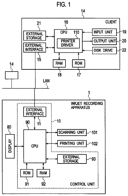
Sheet 1 of 33 from the published document. All sheets in the USPTO PDF
There is provided a communication apparatus comprising an antenna. A communication unit is able to use external power that is generated by receiving a signal from an external apparatus via the antenna, thereby transmitting a response to the signal that is received from the external apparatus to the external apparatus. A deactivation unit deactivates, in a case where the external power is generated by receiving the signal from the external apparatus via the antenna, supply of the external power from the antenna to the communication unit. A control unit performs control so as to interrupt deactivation of supply of the external power from the antenna to the communication unit by the deactivation unit.
Field of the Invention The present invention relates to a communication apparatus, and a method for controlling the same. Description of the Related Art In recent years, wireless communication apparatuses that have a contactless IC reader/writer function have become widely used, and such wireless communication apparatuses can perform wireless communication using a contactless IC with another wireless communication apparatus that is equipped with a contactless IC. Also, wireless communication using a contactless IC is commonly used for exchanging pairing information for other types of wireless communication (for example, Wi-Fi), controlling the operations of a wireless communication apparatus, and the like. The contactless IC can store data in an internal memory, and can perform reading operations in which data in the memory is returned in response to communication from the contactless IC
1 of 33 drawing sheets so far from the published document, cropped to the drawing. Every sheet is in the USPTO PDF.
What the patent claimed, word for word. All of it is now free to use.
Field of the Invention
The present invention relates to a communication apparatus, and a method for controlling the same.
Description of the Related Art
In recent years, wireless communication apparatuses that have a contactless IC reader/writer function have become widely used, and such wireless communication apparatuses can perform wireless communication using a contactless IC with another wireless communication apparatus that is equipped with a contactless IC. Also, wireless communication using a contactless IC is commonly used for exchanging pairing information for other types of wireless communication (for example, Wi-Fi), controlling the operations of a wireless communication apparatus, and the like.
The contactless IC can store data in an internal memory, and can perform reading operations in which data in the memory is returned in response to communication from the contactless IC reader/writer and writing operations in which data is stored in the memory by communication from the contactless IC reader/writer.
The contactless IC can perform wireless communication using only electromagnetic waves from the contactless IC reader/writer as power, and can be used without another power supply. Accordingly, even if the power source of a wireless communication apparatus that is equipped with a contactless IC is in an OFF state, the contactless IC reader/writer can perform reading operations or writing operations on the contactless IC, regardless of an operating state of the wireless communication apparatus.
The capability of responding regardless of the operating state of the wireless communication apparatus is an advantage as well as a disadvantage of the contactless IC. For example, there is a problem in that even in the case where the user does not desire wireless communication using the contactless IC, wireless communication is performed against the user's wishes. Also, for example, there may be a problem in the case where battery capacity for performing Wi-Fi communication is insufficient in a scenario in which pairing information is exchanged and Wi-Fi communication is started, triggered by wireless communication in which the contactless IC is used. In such a case, there is a possibility that, regardless of wireless communication that uses the contactless IC and serves as a trigger having been normally performed, the user will become confused because subsequent Wi-Fi communication does not start.
Japanese Patent Laid-Open No. 2008-92304 proposes a mobile terminal apparatus that sets the contactless IC function to an unusable state in the case where it is conceivable that the user is in a situation where he or she will not use the contactless IC module. This mobile terminal apparatus determines that a user is in a situation where he or she will not use the contactless IC module when the main body of the mobile terminal apparatus is tilted by a predetermined amount or greater, and sets the contactless IC function to an unusable state by stopping power supply to the contactless IC module.
Japanese Patent Laid-Open No. 2008-92304 is directed toward a contactless IC module that requires a separate power supply to electromagnetic waves from the contactless IC reader/writer, and discloses setting the contactless IC function to an unusable state by stopping this power supply. Therefore, the technology in Japanese Patent Laid-Open No. 2008-92304 cannot be applied to a contactless IC that can perform wireless communication using only electromagnetic waves from the contactless IC reader/writer as power.
The present invention has been made in view of such circumstances, and provides technology for controlling activation/deactivation of a wireless communication operation by a contactless IC that can perform wireless communication using, as a power, only electromagnetic waves from a contactless IC reader/writer.
According to an aspect of the present invention, there is provided a communication apparatus comprising: an antenna; a communication unit configured to be able to use external power that is generated by receiving a signal from an external apparatus via the antenna, thereby transmitting a response to the signal that is received from the external apparatus to the external apparatus; a deactivation unit configured to, in a case where the external power is generated by receiving the signal from the external apparatus via the antenna, deactivate supply of the external power from the antenna to the communication unit; and a control unit configured to perform control so as to interrupt deactivation of supply of the external power from the antenna to the communication unit by the deactivation unit.
According to another aspect of the present invention, there is provided a method for controlling a communication apparatus that includes: an antenna; a communication unit configured to be able to use external power that is generated by receiving a signal from an external apparatus via the antenna, thereby transmitting a response to the signal that is received from the external apparatus to the external apparatus; and a deactivation unit configured to, in a case where the external power is generated by receiving the signal from the external apparatus via the antenna, deactivate supply of the external power from the antenna to the communication unit, the control method comprising: a control step of performing control so as to interrupt deactivation of supply of the external power from the antenna to the communication unit by the deactivation unit.
Further features of the present invention will become apparent from the following description of exemplary embodiments with reference to the attached drawings.
FIG. 1 is a block diagram showing a configuration example 1 of peripheral circuits of a contactless IC 102 of a wireless communication apparatus 101 according to a first embodiment.
FIG. 2 is a table of truth values related to states of peripheral circuits of the contactless IC 102 of the wireless communication apparatus 101 according to the first embodiment and a wireless communication operation of the contactless IC 102 .
FIG. 3 is a flowchart showing a procedure for controlling the contactless IC 102 of the wireless communication apparatus 101 according to the first embodiment.
FIG. 4 is a diagram showing an example of a menu for setting operations of the contactless IC 102 of the wireless communication apparatus 101 according to the first embodiment.
FIG. 5 is a block diagram showing a configuration example 2 of peripheral circuits of a contactless IC 502 of the wireless communication apparatus 501 according to the first embodiment.
FIG. 6 is a block diagram showing a configuration example 3 of peripheral circuits of a contactless IC 602 of a wireless communication apparatus 601 according to the first embodiment.
FIG. 7 is a block diagram showing a configuration example 4 of peripheral circuits of a contactless IC 602 of a wireless communication apparatus 701 according to the first embodiment.
FIG. 8 is a block diagram showing a configuration example 1 of peripheral circuits of a contactless IC 102 of a wireless communication apparatus 801 according to a second embodiment.
FIG. 9 is a table of truth values related to states of peripheral circuits of the contactless IC 102 of the wireless communication apparatus 801 according to the second embodiment and the wireless communication operation of the contactless IC 102 .
FIG. 10 is a flowchart showing a procedure for controlling the contactless IC 102 of the wireless communication apparatus 801 according to the second embodiment.
FIG. 11 is a block diagram showing a configuration example 2 of peripheral circuits of a contactless IC 502 of a wireless communication apparatus 1101 according to the second embodiment.
FIG. 12 is a block diagram showing a configuration example 3 of peripheral circuits of a contactless IC 602 of a wireless communication apparatus 1201 according to the second embodiment.
FIG. 13 is a block diagram showing a configuration example 4 of peripheral circuits of a contactless IC 602 of a wireless communication apparatus 1301 according to the second embodiment.
FIG. 14 is a block diagram showing a configuration example 1 of peripheral circuits of a contactless IC 102 of a wireless communication apparatus 1401 according to a third embodiment.
FIG. 15 is a table of truth values related to states of peripheral circuits of the contactless IC 102 of the wireless communication apparatus 1401 according to the third embodiment and the wireless communication operation of the contactless IC 102 .
FIG. 16 is a flowchart showing a procedure for controlling the contactless IC 102 of the wireless communication apparatus 1401 according to the third embodiment.
FIG. 17 is a block diagram showing a configuration example 2 of peripheral circuits of a contactless IC 502 of a wireless communication apparatus 1701 according to the third embodiment.
FIG. 18 is a block diagram showing a configuration example 3 of peripheral circuits of a contactless IC 602 of a wireless communication apparatus 1801 according to the third embodiment.
FIG. 19 is a block diagram showing a configuration example 4 of peripheral circuits of a contactless IC 602 of a wireless communication apparatus 1901 according to the third embodiment.
FIG. 20 is a block diagram showing a configuration example 1 of peripheral circuits of a contactless IC 102 of a wireless communication apparatus 2001 according to a fourth embodiment.
FIG. 21 is a table of truth values related to states of peripheral circuits of the contactless IC 102 of the wireless communication apparatus 2001 according to the fourth embodiment and the wireless communication operation of the contactless IC 102 .
FIG. 22 is a flowchart showing a procedure for controlling the contactless IC 102 of the wireless communication apparatus 2001 according to the fourth embodiment.
FIG. 23 is a block diagram showing a configuration example 2 of peripheral circuits of a contactless IC 502 of a wireless communication apparatus 2301 according to the fourth embodiment.
FIG. 24 is a block diagram showing a configuration example 3 of peripheral circuits of a contactless IC 602 of a wireless communication apparatus 2401 according to the fourth embodiment.
FIG. 25 is a block diagram showing a configuration example 4 of peripheral circuits of a contactless IC 602 of a wireless communication apparatus 2501 according to the fourth embodiment.
FIG. 26 is a block diagram showing the configuration of a wireless communication apparatus 151 that is equipped with a contactless IC reader/writer.
FIG. 27A is a block diagram showing a configuration example 1 of peripheral circuits of the contactless IC 102 of a wireless communication apparatus 2700 according to a fifth embodiment.
FIG. 27B is a block diagram showing a configuration example 2 of peripheral circuits of the contactless IC 502 of a wireless communication apparatus 2801 according to the fifth embodiment.
FIG. 28 is a block diagram showing a configuration example 3 of peripheral circuits of the contactless IC 602 of a wireless communication apparatus 2901 according to the fifth embodiment.
FIG. 29A is a block diagram showing a configuration example 1 of peripheral circuits of the contactless IC 102 of a wireless communication apparatus 3001 according to a sixth embodiment.
FIG. 29B is a block diagram showing a configuration example 2 of peripheral circuits of the contactless IC 502 of a wireless communication apparatus 3101 according to the sixth embodiment.
FIG. 30 is a block diagram showing a configuration example 3 of peripheral circuits of a contactless IC 602 of a wireless communication apparatus 3201 according to the sixth embodiment.
FIG. 31A is a block diagram showing a configuration example 1 of peripheral circuits of the contactless IC 102 of a wireless communication apparatus 3301 according to a seventh embodiment.
FIG. 31B is a block diagram showing a configuration example 2 of peripheral circuits of the contactless IC 502 of a wireless communication apparatus 3401 according to the seventh embodiment.
FIG. 32 is a block diagram showing a configuration example 3 of peripheral circuits of a contactless IC 602 of a wireless communication apparatus 3501 according to the seventh embodiment.
FIG. 33A is a block diagram showing a configuration example 1 of peripheral circuits of the contactless IC 502 of a wireless communication apparatus 3600 according to an eighth embodiment.
FIG. 33B is a block diagram showing a configuration example 2 of peripheral circuits of the contactless IC 502 of a wireless communication apparatus 3701 according to the eighth embodiment.
FIG. 33C is a block diagram showing a configuration example 3 of peripheral circuits of the contactless IC 502 of a wireless communication apparatus 3801 according to the eighth embodiment.
Embodiments of the present invention will now be described with reference to the attached drawings. It should be noted that the technical scope of the present invention is defined by the claims, and is not limited by any of the embodiments described below. In addition, not all combinations of the features described in the embodiments are necessarily required for realizing the present invention.
Also, sizes and shapes of components, relative positions thereof and the like that are illustrated as examples in each embodiment described below are to be appropriately modified depending on the configuration of the apparatus to which the present invention is applied or various conditions, and the present invention is not limited to these examples. First Embodiment
The first embodiment will describe circuits and control methods for switching a wireless communication function of a contactless IC between enabled (usable) and disabled (unusable) in a wireless communication apparatus that is equipped with the contactless IC. Herein, four configuration examples (configuration examples 1 to 4) of circuits that correspond to functions of the contactless IC will be described in order. It is assumed that in the first embodiment, wireless communication of the contactless IC supports the international standard ISO/IEC 21481. Configuration Example 1 of First Embodiment
FIG. 1 is a block diagram showing the configuration example 1 of peripheral circuits of a contactless IC 102 of a wireless communication apparatus 101 according to the first embodiment. In the block diagram that is used to describe the present embodiment, description of a power source connection to blocks that are not necessary for describing the present embodiment will be omitted.
In FIG. 1 , an antenna 103 is an antenna of the contactless IC 102 . The contactless IC 102 can receive electromagnetic waves from a contactless IC reader/writer using the antenna 103 , and perform wireless communication using only external power generated by the electromagnetic waves. In other words, the contactless IC 102 has a power supply function for generating power from the electromagnetic waves received from the antenna 103 and supplying the power for wireless communication, and can be used without another power supply. The contactless IC reader/writer is provided in a wireless communication apparatus 151 such as is shown in FIG. 26 . In FIG. 26 , an antenna 152 is an antenna of the contactless IC reader/writer, and communicates with the antenna 103 of the wireless communication apparatus 101 . Because an internal block diagram of the wireless communication apparatus 151 is not necessary for description of the present embodiment, illustration and description thereof are omitted.
It is assumed that the contactless IC 102 according to the present embodiment has a function of outputting an RF detection signal upon receiving electromagnetic waves and communication from the outside. A power source VDDIN that is supplied to the contactless IC 102 inside the wireless communication apparatus 101 is a power source that is required in the case where a HOST I/F that is a wired interface is operated. In the case where the power source VDDIN is supplied, the contactless IC 102 and a later-described CPU 107 can perform communication via the HOST I/F, and writing/reading of data can be performed to/from the contactless IC 102 . It should be noted that even in the case where the VDDIN is not supplied, the contactless IC 102 can perform wireless communication using only electromagnetic waves from the outside as power.
A battery 104 is a battery of the wireless communication apparatus 101 . A power source IC-A 105 outputs a voltage regardless of the operations of the wireless communication apparatus 101 if the voltage of the battery 104 is in a range in which the power source IC-A 105 operates. A power source IC-B 106 outputs a voltage in accordance with a control signal from the outside.
The CPU 107 (central processing unit) performs overall control of the wireless communication apparatus 101 . A RAM 108 (random access memory) is a memory that is used as a work area of the CPU 107 . A ROM 109 (read only memory) is a memory that stores processing procedures for the CPU 107 , and for example, is constituted by a rewritable non-volatile memory such as a flash memory.
A display unit 110 is constituted by, for example, an LCD (liquid crystal display), and displays video such as image data, operation information, and the like. An operation input unit 111 receives various operations for the wireless communication apparatus 101 , and sends the operation information to the CPU 107 . A memory card 112 can perform writing/reading of digital data.
A wireless communication unit 113 performs wireless communication, and an antenna 114 is an antenna for the wireless communication unit 113 to perform wireless communication. The wireless communication unit 113 supports a wireless standard, which is different from the contactless IC 102 and has a wider communication range. For example, the wireless communication unit 113 supports the WLAN standard IEEE 802.11. Moreover, communication parameters for establishing wireless communication via the wireless communication unit 113 can be shared with the external apparatus via the contactless IC 102 . Specifically, the communication parameters for establishing wireless communication via the wireless communication unit 113 are written in a storage area of the contactless IC 102 in advance, and shared by the external apparatus reading them.
An image capturing unit 115 is constituted by an image sensor and an optical unit that is constituted by a lens and a drive system therefor. An RTC 116 (real time clock) is used to perform clocking. The RTC 116 can continue a backup clocking operation using the voltage output from the power source IC-A 105 even in the case where the main body of the wireless communication apparatus 101 is in the OFF state.
An Ra 120 , an RL 122 , and an Rb 135 are resistors, and an SW-A 121 and an SW-B 123 are switches. An input terminal for turning on/off the SW-A 121 (a first switch) is connected to a terminal for outputting an RF detection signal (a signal output terminal) via the Ra 120 . An input terminal for turning on/off the SW-B 123 (a second switch) is connected to an “output 1 ” of the CPU 107 (a control output terminal) via the Rb 135 . The SW-A 121 and the SW-B 123 can be elements that are in a conduction state when on, and that are in a high impedance state when off, such as an NPN transistor, an NchMOSFET, and the like.
A diode 128 is a diode for rectification. In the case where the SW-A 121 is an NPN transistor, the SW-A 121 itself performs the rectification operation, and therefore the diode 128 is not required, but in the case where the SW-A 121 is an NchMOSFET, the diode 128 for rectification is required. In the present embodiment, because description will be given assuming the SW-A 121 is an NPN transistor, detailed description of the diode 128 will be omitted.
A buffer circuit A 117 buffers an RF detection signal output from the contactless IC 102 and then sends the RF detection signal to the CPU 107 only when the voltage is output from the power source IC-B 106 . Diodes 131 and 132 are arranged in order to perform OR input of signals for controlling the power source IC-B 106 that are sent from both the contactless IC 102 and the CPU 107 .
Next, operations of peripheral circuits of the contactless IC 102 will be described. In the description below, it is assumed that an OFF state of the main body of the wireless communication apparatus 101 refers to a state in which the CPU 107 does not perform control due to the voltage not being output from the power source IC-B 106 and the CPU 107 being in the OFF state. Also, it is assumed that an ON state of the main body of the wireless communication apparatus 101 refers to a state in which the CPU 107 performs control due to the voltage being output from the power source IC-B 106 and the CPU 107 being in the ON state.
First, operations performed in a case in which the contactless IC 102 receives electromagnetic waves and communication from the contactless IC reader/writer in the case where the main body of the wireless communication apparatus 101 is OFF will be described.
The contactless IC 102 outputs a positive logic RF detection signal upon receiving electromagnetic waves and communication from the outside. The RF detection signal drives the SW-A 121 via the Ra 120 , and the SW-A 121 is turned on. The SW-A 121 is connected to the antenna 103 of the contactless IC 102 via the RL 122 , and the antenna 103 is shunted to ground via the RL 122 and the SW-A 121 if the SW-A 121 is ON.
When the antenna 103 is shunted to ground, the electric current generated in the antenna 103 due to the electromagnetic waves from the outside flows to ground side. As a result of the electric current generated in the antenna 103 flowing to ground side, modulation/demodulation for wireless communication in the contactless IC 102 is prevented, and the power required to perform wireless communication cannot be maintained, as a result of which the wireless communication operation is stopped. In order to reliably prevent modulation/demodulation for wireless communication, it is desirable that the RL 122 and the SW-A 121 are connected to an antenna terminal on the side to which the load that is used to perform wireless communication load modulation in the contactless IC 102 is connected so as to extract the electric current of the antenna 103 .
Upon receiving electromagnetic waves and communication from the outside, the contactless IC 102 outputs an RF detection signal, and thus drives the power source IC-B 106 using the RF detection signal. Thereafter, the CPU 107 starts operating with the voltage output from the power source IC-B 106 . However, as described above, if the contactless IC 102 cannot maintain the power required to perform wireless communication and the wireless communication operation stops, the contactless IC 102 stops output of the RF detection signal, and therefore the power source IC-B 106 is no longer driven by the contactless IC 102 .
Next, operations performed in the case in which the contactless IC 102 receives electromagnetic waves and communication from the contactless IC reader/writer in the case where the main body of the wireless communication apparatus 101 is ON will be described.
In the case where the main body of the wireless communication apparatus 101 is ON, the wireless communication apparatus 101 can drive the SW-B 123 using a signal from the CPU 107 (an output 1 ). If the SW-B 123 is driven by the signal from the CPU 107 and the SW-B 123 is turned on, the SW-B 123 shunts the signal that drives the SW-A 121 to ground, as a result of which the SW-A 121 is turned off.
In the case where the SW-B 123 is turned on under the control of the CPU 107 , the contactless IC 102 outputs the RF detection signal upon receiving electromagnetic waves and communication from the outside, but the RF detection signal is shunted to ground by the SW-B 123 via the Ra 120 . Accordingly, the SW-A 121 is not driven by the RF detection signal, and the SW-A 121 is turned off. If the SW-A 121 is in the OFF state, the contactless IC 102 can perform wireless communication.
The operations of the configuration example 1 of the first embodiment are summarized as follows.
In the case where the main body of the wireless communication apparatus 101 is OFF, the SW-A 121 is turned on when the contactless IC receives electromagnetic waves and communication from the outside, and the antenna 103 is shunted to ground via the SW-A 121 , and therefore the wireless communication operation of the contactless IC 102 is deactivated.
In the case where the main body of the wireless communication apparatus 101 is ON, the wireless communication apparatus 101 can perform control to turn on/off the SW-B 123 using a signal from the CPU 107 (the output 1 ). Because the SW-A 121 is OFF even if the contactless IC receives electromagnetic waves and communication from the outside in the case where the SW-B 123 is ON, the wireless communication operation of the contactless IC 102 is activated. When the contactless IC receives electromagnetic waves and communication from the outside in the case where the SW-B 123 is OFF, the SW-A 121 is turned on, and the wireless communication operation of the contactless IC 102 is deactivated.
Control for switching the wireless communication of the contactless IC 102 between enabled and disabled has been described above with regard to the respective cases in which the main body of the wireless communication apparatus 101 is OFF and ON.
FIG. 2 is a table of truth values related to states of peripheral circuits of the contactless IC 102 of the wireless communication apparatus 101 according to the first embodiment and the wireless communication operation of the contactless IC 102 . In the description below, activation and deactivation of the wireless communication operation of the contactless IC 102 may be respectively described as “enabling” and “disabling” the wireless communication operation.
If the operation minimum voltage of the power source IC-B 106 is Vb 1 , the power source IC-B 106 cannot operate in the case where a battery voltage Vbatt of the battery 104 is 0≦Vbatt<Vb 1 , and therefore the CPU 107 is OFF. If the CPU 107 is OFF, the wireless communication operation of the contactless IC 102 is only “disabled”.
In the case where the battery voltage Vbatt of the battery 104 is Vb 1 ≦Vbatt, the power source IC-B 106 is operable, and therefore the CPU 107 can be in either the ON or the OFF state. Although if the CPU 107 is OFF, the wireless communication operation of the contactless IC 102 is “disabled”, if the CPU 107 is ON, the wireless communication operation of the contactless IC 102 can be selectively “disabled” or “enabled” under the control of the CPU 107 .
FIG. 3 is a flowchart showing the procedure for controlling the contactless IC 102 of the wireless communication apparatus 101 according to the first embodiment. Processing of each step in this flowchart is executed by the CPU 107 , unless otherwise stated.
The CPU 107 determines in step S 101 whether or not the wireless communication operation setting of the contactless IC 102 is activated. Activation/deactivation of the wireless communication operation setting can be switched by a user using the display unit 110 and the operation input unit 111 . If a user operates the operation input unit 111 so as to give an instruction to display a menu for setting operations of the contactless IC 102 , the CPU 107 displays an operation setting menu such as is shown in FIG. 4 on the display unit 110 , for example. The user selects “activate” or “deactivate” by operating the operation input unit 111 in the operation setting menu to switch the wireless communication operation setting between activation and deactivation. The switching of activation/deactivation may be protected by a lock function using a password.
In the case where it is determined in step S 101 that the wireless communication operation setting is not activated, in step S 102 , the CPU 107 controls the output 1 to “L” so as to turn off the SW-B 123 , and thereby causes the contactless IC 102 to be “disabled”.
In the case where it is determined in step S 101 that the wireless communication operation setting is activated, the CPU 107 determines in step S 103 whether or not the operation mode of the CPU 107 is a mode in which the contactless IC 102 can perform wireless communication. The mode in which the contactless IC 102 cannot perform wireless communication is a mode in which the processing load of the CPU 107 is too high to process communication using the contactless IC 102 such as, for example, when the wireless communication apparatus 101 controls the image capturing unit 115 to capture a still image or a moving image. In other words, in step S 103 , conditional branching is performed in accordance with whether or not the processing load of the CPU 107 is greater than or equal to a threshold.
In the case where it is determined in step S 103 that the operation mode of the CPU 107 is a mode in which the contactless IC 102 cannot perform wireless communication, in step S 102 , the CPU 107 controls the output 1 to “L” to turn off the SW-B 123 , and thereby causes the contactless IC 102 to be “disabled”.
In the case where it is determined in step S 103 the operation mode of the CPU 107 is a mode in which the contactless IC 102 can perform wireless communication, in step S 104 , the CPU 107 controls the output 1 to “H” to turn on the SW-B 123 , and thereby causes the contactless IC 102 to be “enabled”.
The CPU 107 determines in step S 105 whether or not an operation for turning off the power source of the wireless communication apparatus 101 has been performed using the operation input unit 111 . If the operation for turning off the power source has not been performed, the processing returns to step S 101 . In the case where the operation for turning off the power source has been performed, the CPU 107 ends the processing of this flowchart.
In this manner, in the present embodiment, in the case where the CPU 107 is ON, the wireless communication operation of the contactless IC 102 can be set to either “disabled” or “enabled” depending on the wireless communication operation setting of the contactless IC 102 (step S 101 ). If the wireless communication operation setting of the contactless IC 102 is stored in the ROM 109 , when the wireless communication apparatus 101 is turned on, the CPU 107 can read out the wireless communication operation setting of the contactless IC 102 stored in the ROM 109 , and control the wireless communication operation of the contactless IC 102 . Configuration Example 2 of First Embodiment
FIG. 5 is a block diagram showing the configuration example 2 of peripheral circuits of a contactless IC 502 of a wireless communication apparatus 501 according to the first embodiment. In FIG. 5 , the same reference numerals are given to constituent elements that are the same as or similar to those in the configuration example 1 of FIG. 1 . Hereinafter, differences from the configuration example 1 will be mainly described.
The function of the contactless IC 502 is different from the function of the contactless IC 102 in FIG. 1 . The contactless IC 102 of FIG. 1 outputs a positive logic RF detection signal upon receiving electromagnetic waves and communication from the outside, whereas the contactless IC 502 of FIG. 5 outputs a negative logic RF detection signal upon receiving electromagnetic waves and communication from the outside. Similarly to the contactless IC 102 , the contactless IC 502 can receive electromagnetic waves from the contactless IC reader/writer using the antenna 103 , and perform wireless communication using only electromagnetic waves as power. In other words, the contactless IC 502 has a power supply function for generating power from the electromagnetic waves received from the antenna 103 and supplying power for wireless communication, and can be used without another power supply.
An inverter circuit A 517 inverts the signal logic to match the function of the contactless IC 502 and the peripheral circuits. Other functions of the inverter circuit A 517 are similar to the buffer circuit A 117 in FIG. 1 . An inverter circuit B 530 inverts the signal logic to match the function of the contactless IC 502 and the peripheral circuits.
An input terminal for turning on/off the SW-A 121 (a first switch) is connected to the antenna 103 via the Ra 120 and the diode 526 . An input terminal for turning on/off the SW-B 123 (a second switch) is connected to an “output 1 ” of the CPU 107 (a control output terminal) via the Rb 135 .
When the contactless IC 502 receives electromagnetic waves from the outside, the electric current is generated in the antenna 103 , and the electric current is rectified by the diode 526 . The rectified electric current drives the SW-A 121 via the Ra 120 , and the SW-A 121 is turned on. A CL 527 is a capacitor, and is disposed for compensating driving of the SW-A 121 . The SW-A 121 is connected to the antenna 103 of the contactless IC 502 via the RL 122 , and the antenna 103 is shunted to ground via the RL 122 and the SW-A 121 if the SW-A 121 is ON.
When the antenna 103 is shunted to ground, the electric current generated in the antenna 103 due to the electromagnetic waves from the outside flows to the ground side. As a result of the electric current generated in the antenna 103 flowing in the ground side, modulation/demodulation for wireless communication in the contactless IC 502 is prevented, and the power required to perform wireless communication cannot be maintained, as a result of which the wireless communication operation is stopped. In order to reliably prevent modulation/demodulation for wireless communication, it is desirable that the RL 122 and the SW-A 121 are connected to an antenna terminal on the side to which the load that is used to perform wireless communication load modulation in the contactless IC 502 is connected so as to extract the electric current of the antenna 103 .
The configuration example 2 of FIG. 5 and the configuration example 1 of FIG. 1 are the same in that they have the SW-A 121 and the SW-B 123 . Therefore, also in the configuration example 2, the wireless communication operation of the contactless IC 502 can be selectively “disabled” or “enabled” under the control of the CPU 107 . The table of truth values in FIG. 2 , the flowchart in FIG. 3 , and the operation setting menu in FIG. 4 can also be applied to the configuration example 2. Configuration Example 3 of First Embodiment
FIG. 6 is a block diagram showing the configuration example 3 of peripheral circuits of a contactless IC 602 of a wireless communication apparatus 601 according to the first embodiment. In FIG. 6 , the same reference numerals are given to constituent elements that are the same as or similar to those in the configuration example 1 of FIG. 1 and the configuration example 2 of FIG. 5 . Hereinafter, differences from the configuration examples 1 and 2 will be mainly described.
The function of the contactless IC 602 is different from the function of the contactless IC 502 in FIG. 5 . Upon receiving electromagnetic waves from the outside, the contactless IC 502 in FIG. 5 internally uses the electromagnetic waves as power for operating wireless communication. In contrast, upon receiving electromagnetic waves from the outside, the contactless IC 602 of FIG. 6 outputs a voltage to a VDD terminal, and accumulates the voltage required to perform wireless communication in an operation compensate capacitor Ca 625 to perform wireless communication. Similarly to the contactless IC 502 , the contactless IC 602 can receive electromagnetic waves from the contactless IC reader/writer using the antenna 103 , and perform wireless communication using only electromagnetic waves as power. In other words, the contactless IC 602 has a power supply function for generating power from the electromagnetic waves received from the antenna 103 and supplying the power for wireless communication, and can be used without another power supply.
An input terminal for turning on/off the SW-A 121 (a first switch) is connected to the VDD terminal (a power output terminal) via the Ra 120 . An input terminal for turning on/off the SW-B 123 (a second switch) is connected to an “output 1 ” of the CPU 107 (a control output terminal) via the Rb 135 .
The contactless IC 602 outputs a voltage to the VDD terminal upon receiving electromagnetic waves and communication from the outside. The signal generated by the voltage that is output to the VDD terminal drives the SW-A 121 via the Ra 120 , and the SW-A 121 is turned on. The SW-A 121 is connected to the antenna 103 for the contactless IC 602 via the RL 122 , and the antenna 103 is shunted to ground via the RL 122 and the SW-A 121 if the SW-A 121 is ON.
When the antenna 103 is shunted to ground, the electric current generated in the antenna 103 due to the electromagnetic waves from the outside flows to the ground side. As a result of the electric current generated in the antenna 103 flowing in the ground side, modulation/demodulation for wireless communication in the contactless IC 602 is prevented, and the power required to perform wireless communication cannot be maintained, as a result of which the wireless communication operation is stopped. In order to reliably prevent modulation/demodulation for wireless communication, it is desirable that the RL 122 and the SW-A 121 are connected to an antenna terminal on the side to which the load that is used to perform wireless communication load modulation in the contactless IC 602 is connected so as to extract the electric current of the antenna 103 .
The configuration example 3 of FIG. 6 and the configuration example 1 of FIG. 1 are the same in that they have the SW-A 121 and the SW-B 123 . Therefore, also in the configuration example 3, the wireless communication operation of the contactless IC 602 can be selectively “disabled” or “enabled” under the control of the CPU 107 . The table of truth values in FIG. 2 , the flowchart in FIG. 3 , and the operation setting menu in FIG. 4 can also be applied to the configuration example 3. Configuration Example 4 of First Embodiment
FIG. 7 is a block diagram showing the configuration example 4 of peripheral circuits of a contactless IC 602 of a wireless communication apparatus 701 according to the first embodiment. In FIG. 7 , the same reference numerals are given to constituent elements that are the same as or similar to those in the configuration example 1 of FIG. 1 , the configuration example 2 of FIG. 5 , and the configuration example 3 of FIG. 6 . Hereinafter, differences from the configuration examples 1, 2, and 3 will be mainly described.
An input terminal for turning on/off the SW-A 121 (a first switch) is connected to the antenna 103 via the Ra 120 and a diode 726 . An input terminal for turning on/off the SW-B 123 (a second switch) is connected to an “output 1 ” of the CPU 107 (a control output terminal) via the Rb 135 .
When the contactless IC 602 receives electromagnetic waves from the outside, the electric current is generated in the antenna 103 , and the electric current is rectified by the diode 726 . The rectified electric current drives the SW-A 121 via the Ra 120 , and the SW-A 121 is turned on. A CL 727 is the capacitor, and is disposed for compensating driving of the SW-A 121 . The SW-A 121 is connected to the VDD terminal of the contactless IC 602 via the RL 122 , and if the SW-A 121 is ON, the VDD terminal of the contactless IC 602 is shunted to ground via the RL 122 and the SW-A 121 .
The description continues in the full USPTO document.
About 6,713 words. The USPTO PDF has it with every drawing.
Fees are due 3.5, 7.5 and 11.5 years after grant. This patent expired on September 12, 2025, so the fee marked "not paid" was the one that went unpaid.
COMMUNICATION APPARATUS AND METHOD FOR CONTROLLING THE SAME
Filed Feb 2016 · published Jun 2016Communication apparatus and method for controlling the same
Filed Feb 2016 · granted Sep 2017Earlier publications, parents and continuations. None of them can still be enforced, or this patent would not be listed.
Prior art cited by the examiner or applicant. Useful when you check your own idea for novelty.
Everything on this page comes from the documents linked above.