Technical field
The subject disclosure relates to electromagnetic (EM) wave mode transducers, e.g., to EM wave mode transition or transducer structures, and related devices, techniques, and methods.
Background
Microwave and millimeter wave circuits (e.g., such as those associated with wideband planar baluns, filters, and antenna systems, etc.) and associated systems (e.g., wireless communication systems, etc.) can employ waveguides such as substrate integrated waveguides (SIWs), laminated waveguides, or post-wall waveguides, which can be considered as waveguides integrated in substrates. Conventional SIWs have been demonstrated in the various applications of filters, power combiners and dividers, couplers, antennas, and so on. However, transitions or transducers between SIWs and other transmission lines require particular performance and design considerations as well as component integration considerations.
In addition, conventional wideband transitions or transducers from planar transmission lines to SIW are typically designed for the dominant mode of SIW, namely, the transverse electric mode 10 (TE.sub.10 mode). However, as SIW deployment in electronic systems increases, higher order mode (e.g., transverse electric mode 20 (TE.sub.20 mode), etc.) components associated with SIWs have become the subject of increasing research. For instance, conventional higher order mode SIW components for antenna systems operating in millimeter wave bands have been proposed.
However, limitations of various conventional transition or transducer structures or feeding technologies exist. For example, conventional transition or transducer structures for higher order mode SIW components are complex, thereby increasing fabrication costs, the bandwidth of conventional transition or transducer structures is relatively narrow, and so on. Accordingly, improvements that provide a wideband direct transition or transducer to higher order mode waveguides should simplify the transition or transducer structures, with associated reductions in fabrication cost, and should enhance performance stability of the transition or transducer structures by incorporating relaxed fabrication tolerances.
The subject disclosure provides embodiments that improve upon these and other deficiencies. The above-described deficiencies of conventional transition or transducer structures for higher order mode waveguide components are merely intended to provide an overview of some of the problems of conventional implementations, and are not intended to be exhaustive. Other problems with conventional implementations and techniques and corresponding benefits of the various non-limiting embodiments described herein may become further apparent upon review of the following description.
Summary
The following presents a simplified summary of the specification to provide a basic understanding of some aspects of the specification. This summary is not an extensive overview of the specification. It is intended to neither identify key or critical elements of the specification nor delineate any scope particular to any embodiments of the specification, or any scope of the claims. Its sole purpose is to present some concepts of the specification in a simplified form as a prelude to the more detailed description that is presented later.
In various non-limiting embodiments of the subject disclosure, EM wave mode transition or transducer structures, and related devices, techniques, and methods are provided. For instance, non-limiting implementations provide exemplary devices comprising an EM mode transducer configured as an EM mode transition between a fundamental mode transmission line and a TE.sub.20 mode waveguide. As a non-limiting example, various implementations of the exemplary devices can comprise a cavity section, such as an over-moded waveguide cavity section, configured to propagate or excite more than one mode of EM waves over a selected operation frequency band, such as the X-band, or portions thereof. In further non-limiting examples, exemplary devices can comprise a fundamental mode rejection section of the EM mode transducer.
Additionally, in various embodiments of the subject disclosure, exemplary apparatuses can comprise means for transmitting or receiving EM waves to or from a fundamental mode transmission line, means for suppressing a transverse electric mode 30 (TE.sub.30 mode) of the EM waves, means for reflecting or suppressing a TE.sub.10 mode of the EM waves, and means for controlling propagation of a TE.sub.20 mode of the EM waves from the fundamental mode transmission line.
In other non-limiting implementations, exemplary methods associated with various non-limiting embodiments of EM wave mode transition or transducer structures and related devices are provided.
These and other embodiments are described in more detail below.
Brief description of the drawings
Various non-limiting embodiments are further described with reference to the accompanying drawings in which:
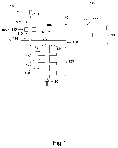
FIG. 1 depicts a top view of an exemplary electromagnetic (EM) mode transition or transducer structure, according to non-limiting aspects of the subject disclosure;
FIG. 2 depicts a three-dimensional view of an exemplary EM mode transition or transducer structure, according to further aspects of the subject disclosure;
FIG. 3 depicts another three-dimensional view of an exemplary EM mode transition or transducer structure;
FIG. 4 depicts a top view of another exemplary EM mode transition or transducer structure, according to further non-limiting aspects;
FIG. 5 depicts a three-dimensional view of an exemplary EM mode transition or transducer structure, according to further aspects of the subject disclosure;
FIG. 6 depicts another three-dimensional view of an exemplary EM mode transition or transducer structure;
FIG. 7 depicts a top view of further exemplary EM mode transition or transducer structure, according to still further non-limiting aspects;
FIG. 8 demonstrates non-limiting aspects of transition performance for an exemplary EM mode transition or transducer structure of FIG. 7 ;
FIG. 9 depicts non-limiting electric field distributions for an exemplary EM mode transition or transducer structure of FIG. 7 at a frequency of 8.5 GigaHertz (GHz);
FIG. 10 depicts non-limiting electric field distributions for an exemplary EM mode transition or transducer structure of FIG. 7 at a frequency of 9.7 GHz;
FIG. 11 depicts non-limiting electric field distributions for an exemplary EM mode transition or transducer structure of FIG. 7 at a frequency of 11 GHz;
FIG. 12 depicts a top view of another exemplary EM mode transition or transducer structure, according to non-limiting aspects of the subject disclosure;
FIG. 13 demonstrates non-limiting aspects of transition performance for an exemplary EM mode transition or transducer structure of FIG. 12 ;
FIG. 14 depicts non-limiting electric field distributions for an exemplary EM mode transition or transducer structure of FIG. 12 at a frequency of 8.0 GHz;
FIG. 15 depicts non-limiting electric field distributions for an exemplary EM mode transition or transducer structure of FIG. 12 at a frequency of 9.5 GHz;
FIG. 16 depicts non-limiting electric field distributions for an exemplary EM mode transition or transducer structure of FIG. 12 at a frequency of 11 GHz;
FIG. 17 depicts a top view of another exemplary EM mode transition or transducer structure, according to non-limiting aspects of the subject disclosure;
FIG. 18 demonstrates non-limiting aspects of transition performance for an exemplary EM mode transition or transducer structure of FIG. 17 ;
FIG. 19 depicts a top view of a further exemplary EM mode transition or transducer structure, according to further non-limiting aspects;
FIG. 20 demonstrates non-limiting aspects of transition performance for an exemplary EM mode transition or transducer structure of FIG. 19 ;
FIG. 21 depicts a top view of yet another exemplary EM mode transition or transducer structure, according to non-limiting aspects of the subject disclosure;
FIG. 22 demonstrates non-limiting aspects of transition performance for an exemplary EM mode transition or transducer structure of FIG. 21 ;
FIG. 23 depicts an exemplary flowchart of non-limiting methods associated with various non-limiting embodiments of the subject disclosure; and
FIG. 24 depicts an exemplary flowchart of further non-limiting methods associated with various non-limiting embodiments of the subject disclosure. DETAILED DESCRIPTION Overview
While a brief overview is provided, certain aspects of the subject disclosure are described or depicted herein for the purposes of illustration and not limitation. Thus, variations of the disclosed embodiments as suggested by the disclosed apparatuses, systems and methodologies are intended to be encompassed within the scope of the subject matter disclosed herein. For example, the various embodiments of the apparatuses, techniques and methods of the subject disclosure are described in the context of EM mode transducer or transition structures. However, as further detailed below, various exemplary implementations can be applied to other areas associated with waveguides, without departing from the subject matter described herein. Furthermore, while various embodiments of the subject disclosure may be described in the context of a particular direction of wave propagation, it is to be appreciated that, as passive devices, the opposite direction of wave propagation is also possible without deviating from the scope of the described embodiments. As a non-limiting example, where EM waves are described as propagating from a fundamental mode transmission line to a TE.sub.20 mode waveguide, it is to be appreciated that EM waves can also be propagated from the TE.sub.20 mode waveguide to the fundamental mode transmission line using the described embodiments.
As used herein, the term, “over-moded,” in reference to a waveguide, a component related thereto, or portion thereof, can refer to a component, or portion thereof, that can be configured to propagate or excite more than one mode of EM waves over a selected or predetermined operation frequency band. As further used herein, the terms “substrate integrated waveguide (SIW)”, “laminated waveguides,” or “post-wall waveguides,” can refer to waveguides integrated in substrates, according to conventional integration and/or fabrication techniques.
As described in the background, as SIW deployment in electronic systems increases, higher order mode (e.g., TE.sub.20 mode, etc.) components associated with SIWs have become the subject of increasing research. For instance, conventional higher order mode SIW components for antenna systems operating in millimeter wave bands have been proposed. However, conventional transition or transducer structures for higher order mode SIW components are complex, thereby increasing fabrication costs, the bandwidth of conventional transition or transducer structures is relatively narrow, and so on. Accordingly, improvements to conventional transition or transducer structures for higher order mode SIW components as described herein can provide a wideband direct transition or transducer for higher order mode waveguides.
For instance, practical wideband planar higher order EM mode transition or transducer structures, as described herein, can be employed in wideband EM mode transitions between a fundamental mode transmission line and a higher order mode (e.g., TE.sub.20 mode, etc.) waveguide. According to non-limiting embodiments of the subject disclosure, exemplary EM mode transition or transducer structures can comprise a waveguide cavity section (e.g., an over-moded waveguide cavity section, etc.). In further non-limiting embodiments, exemplary EM mode transition or transducer structures can further comprise a fundamental mode rejection section.
According to various non-limiting aspects, exemplary embodiments, as described herein, can simplify EM mode transition or transducer structures, with associated reductions in fabrication cost. In addition, according to further aspects of the subject disclosure, various embodiments as described herein can enhance performance stability of exemplary EM mode transition or transducer structures by incorporating various non-limiting aspects that can be resilient to variations in fabrication processes. In addition, various aspects of the exemplary EM mode transition or transducer structures, as described herein, can be employed in substrate integrated circuits, metal waveguide devices, and so on.
In contrast to typical TE.sub.20 EM mode transition or transducer structures based on conventional multilayer technologies or defected ground metal structures, various aspects of exemplary EM mode transition or transducer structures, as described herein, can comprise a planar structure without employing defecting ground metal structures. As a result, exemplary EM mode transition or transducer structures, as described herein, can provide convenient methods of integration or fabrication in associated apparatuses or articles of manufacture. Moreover, as compared with conventional technologies for waveguide direct feeding, exemplary EM mode transition or transducer structures, as described herein, can facilitate providing wider bandwidth EM mode transition or transducer structures, can facilitate impedance matching, and can facilitate fundamental mode rejection of EM waves. In addition, various aspects of the exemplary EM mode transition or transducer structures, as described herein, can be employed in substrate integrated circuits, metal waveguide devices, and so on.
According to further non-limiting aspects, exemplary EM mode transition or transducer structures, as described herein, can facilitate directly feeding an associated TE.sub.20 mode waveguide by a microstrip line, a waveguide, a coplanar waveguide (CPW), and so on, as further described herein. For instance, as exemplified herein, exemplary EM mode transition or transducer structures to a TE.sub.20 mode substrate integrated waveguide from microstrip line, SIW, and CPW can facilitate wideband planar baluns, filters, and antenna feeding networks.
Various aspects or features of the subject disclosure are described with reference to the drawings, wherein like reference numerals are used to refer to like elements throughout. In this specification, numerous specific details are set forth in order to provide a thorough understanding of the subject disclosure. It should be understood, however, that the certain aspects of disclosure may be practiced without these specific details, or with other methods, components, parameters, etc. In other instances, well-known structures and devices can be shown in block diagram form to facilitate description and illustration of the various embodiments. In accordance with one or more embodiments described in subject disclosure, exemplary EM mode transition or transducer structures, and related devices, techniques, and methods are provided.
While, for the purposes of illustration, and not limitation, various non-limiting implementations of the subject disclosure are described herein in reference to EM mode transition or transducer structures and so on, it can be understood that variations of the subject disclosure are possible within the scope of claims appended to the subject matter disclosed herein. Thus, it can be understood that particular aspects of exemplary EM mode transition or transducer structures and so on, as described herein, can be employed or be desirable in conjunction with particular circuits, systems, components, and/or combination, variations and/or portions thereof, associated with the subject disclosure, depending on, for example, design considerations, etc. For instance, particular non-limiting aspects of exemplary EM mode transition or transducer structures, as described in reference to FIGS. 1-6 , for example, can provide an EM mode transition between a fundamental mode transmission line and a TE.sub.20 mode waveguide. Exemplary Embodiments
Accordingly, FIG. 1 depicts a top view of an exemplary EM mode transition or transducer structure 100 , according to non-limiting aspects of the subject disclosure. FIG. 2 depicts a three-dimensional view 200 of an exemplary EM mode transition or transducer structure 100 , according to further aspects of the subject disclosure, whereas FIG. 3 depicts another three-dimensional view 300 of an exemplary EM mode transition or transducer structure 100 . According to non-limiting embodiments of the subject disclosure, exemplary EM mode transition or transducer structure 100 can comprise a waveguide cavity section 102 (e.g., an over-moded waveguide cavity section 102 , etc.). In further non-limiting embodiments, exemplary EM mode transition or transducer structure 100 can further comprise a fundamental mode rejection section 104 .
In addition, exemplary EM mode transition or transducer structure 100 can further comprise a first port 106 that connects a fundamental mode transmission line (not shown) to the a waveguide cavity section 102 (e.g., an over-moded waveguide cavity section 102 , etc.) of the exemplary EM mode transition or transducer structure 100 . In further non-limiting aspects, exemplary EM mode transition or transducer structure 100 can also comprise a second port 108 located proximate to the fundamental mode rejection section 104 and opposite the waveguide cavity section 102 (e.g., an over-moded waveguide cavity section 102 , etc.). In various non-limiting aspects, first port 106 can connect a fundamental mode transmission line (not shown) comprising a microstrip transmission line, a strip line, a waveguide, a CPW, and the like, as further described herein. According to further non-limiting aspects, the second port 108 can be configured to propagate a TE.sub.20 mode of EM waves to a TE.sub.20 mode waveguide (not shown) connected at the second port 108 .
In various non-limiting implementations, exemplary EM mode transition or transducer structure 100 can comprise a top substrate sheet 110 and a bottom substrate sheet 112 comprising a metallic substance. Thus, top substrate sheet 110 and bottom substrate sheet 112 can comprise a top substrate metal sheet 110 and a bottom substrate metal sheet 112 , as further described herein. In further non-limiting implementations, EM mode transition or transducer structure 100 can further comprise a set of metallic sidewalls 114 (e.g., narrow metallic sidewalls 114 , etc.) that can support top substrate metal sheet 110 and bottom substrate metal sheet 112 . In still further non-limiting implementations, EM mode transition or transducer structure 100 can comprise a set of metallic sidewall posts that can support top substrate metal sheet 110 and bottom substrate metal sheet 112 , as further described herein.
According to a non-limiting aspect, width W 1 116 of a fundamental mode rejection section (e.g., fundamental mode rejection section 104 , etc.) of the exemplary EM mode transition or transducer structure 100 can be selected (and a fundamental mode rejection section 104 configured thereby) among a range of widths W 1 116 of a fundamental mode rejection section 104 that can facilitate cutting off TE.sub.30 modes in a selected operation frequency band, thereby allowing transmission of the TE.sub.20 mode of EM waves while suppressing the TE.sub.30 mode. Accordingly, a fundamental mode rejection section 104 of exemplary EM mode transition or transducer structure 100 can be configured for TE.sub.20 mode transmission and TE.sub.30 mode suppression. For instance, a waveguide cut off frequency, for a general TE.sub.n0 mode, when the EM wave frequency is lower than the waveguide cut off frequency, the EM wave will propagate in the waveguide. Thus, by selecting waveguide width (e.g., width of W 1 116 ) for a particular TE.sub.n0 mode to be smaller than the cut off waveguide width of a TE.sub.30 mode, TE.sub.30 mode of the EM wave will not be propagated in the waveguide having a width of W 1 116 .
Accordingly, as a non-limiting example, W 1 116 selected for fundamental mode rejection section 104 can be larger than a width value that can be determined to cut off TE.sub.20 mode of the lowest frequency in a selected operation frequency band, such as, for example, the X band (e.g., EM waves having a frequency range of about 7 GHz to about 11.2 GHz, etc.), or a subset thereof, for exemplary EM mode transition or transducer structure 100 , but less than a width value that can be determined to cut off TE.sub.30 mode in the selected operation frequency band. Thus, in a particular non-limiting implementation of the subject disclosure, an exemplary EM mode transition or transducer structure 100 can provide a wideband EM mode transition or transducer structure 100 comprising a fundamental mode rejection section 104 , according to considerations of multiple frequencies of the TE.sub.201 mode resonance.
In further non-limiting aspects, exemplary EM mode transition or transducer structure 100 can further comprise an array of metallic posts 118 located proximate to a centerline 120 of the fundamental mode rejection section 104 . As a non-limiting example, an array of cylindrical metallic posts 118 array can be oriented in a longitudinal direction of exemplary EM mode transition or transducer structure 100 . In a further non-limiting example, metallic posts 118 can be configured to traverse the distance between top substrate metal sheet 110 and a bottom substrate metal sheet 112 , as depicted in FIGS. 1-3 , and as further described herein. Accordingly, metallic posts 118 located proximate to a centerline 120 of the fundamental mode rejection section 104 can facilitate suppressing the fundamental mode of EM waves in the fundamental mode rejection section 104 of exemplary EM mode transition or transducer structure 100 . In addition, an array of metallic posts (e.g., an array of metallic posts 118 , etc.) located proximate to a centerline 120 of the fundamental mode rejection section (e.g., fundamental mode rejection section 104 , etc.) can facilitate suppressing the TE.sub.30 mode. In further non-limiting aspects, metallic posts 118 can comprise metallic posts having a cross section other than a cylindrical cross section, for example, such as elliptic, square, triangular, rectangular, pentagonal, hexagonal, and so on, without limitation. In yet another non-limiting aspect, the distance between any two neighboring metallic posts 118 in the fundamental mode rejection section 104 can be configured to be less than one guided wavelength. In still further non-limiting aspects, a waveguide cavity section 102 (e.g., an over-moded waveguide cavity section 102 , etc.) of exemplary EM mode transition or transducer structure 100 can further comprise a set of impedance matching metallic posts 122 , as further described herein.
As a result, according to various non-limiting embodiments of the subject disclosure, when an EM field in the selected operation frequency band is incident to exemplary EM mode transition or transducer structure 100 from the first port 106 , TE.sub.20 and TE.sub.10 modes can be excited in a waveguide cavity section 102 (e.g., an over-moded waveguide cavity section 102 , etc.). In addition, according to various aspects, a fundamental mode, e.g., TE.sub.10 mode, can be reflected back and/or suppressed by the metallic posts 118 in fundamental mode rejection section 104 . As a result, the symmetrical plane of exemplary EM mode transition or transducer structure 100 in a transition to a TE.sub.20 mode waveguide (not shown) can be considered as an electric wall, such that cylindrical metallic posts 118 in the rejection section have few impacts on the TE.sub.20 mode transmission. Thus, when the EM field is transmitted to the second port 108 , only TE.sub.20 mode exists, for example, as further described herein.
As a result, exemplary EM mode transition or transducer structure 100 can provide wideband EM wave mode transition between fundamental mode transmission line (not shown) and TE.sub.20 mode waveguide (not shown). As further described above, exemplary EM mode transition or transducer structure 100 can directly feed a TE.sub.20 mode waveguide from a microstrip transmission line, a strip line, a waveguide, a CPW, and so on, which can be employed in any of a number of applications involving microwave and/or millimeter wave higher order mode substrate integrated circuits, metal waveguide devices, and so on, such as planar baluns, filters, and antenna feeding networks.
FIG. 4 depicts a top view of another exemplary EM mode transition or transducer structure 400 , according to further non-limiting aspects. FIG. 5 depicts a three-dimensional view of an exemplary EM mode transition or transducer structure 400 , according to further aspects of the subject disclosure, whereas FIG. 6 depicts another three-dimensional view of an exemplary EM mode transition or transducer structure 400 . According to non-limiting embodiments of the subject disclosure, exemplary EM mode transition or transducer structure 400 can comprise a waveguide cavity section 402 (e.g., an over-moded waveguide cavity section 402 , etc.). In further non-limiting embodiments, exemplary EM mode transition or transducer structure 400 can further comprise a fundamental mode rejection section 404 . In addition, exemplary EM mode transition or transducer structure 400 can further comprise a first port 406 that connects a fundamental mode transmission line (not shown) to the a waveguide cavity section 402 (e.g., an over-moded waveguide cavity section 402 , etc.) of the exemplary EM mode transition or transducer structure 400 .
In further non-limiting aspects, exemplary EM mode transition or transducer structure 400 can also comprise a second port 408 located proximate to the fundamental mode rejection section 404 and opposite the waveguide cavity section 402 (e.g., an over-moded waveguide cavity section 402 , etc.). In various non-limiting aspects, first port 406 can connect a fundamental mode transmission line (not shown) comprising a microstrip transmission line, a strip line, a waveguide, a CPW, and the like, as further described herein. According to further non-limiting aspects, the second port 408 can be configured to propagate a TE.sub.20 mode of EM waves to a TE.sub.20 mode waveguide (not shown) connected at the second port 408 .
As further described above, exemplary EM mode transition or transducer structure 400 can comprise a top substrate sheet 410 and a bottom substrate sheet 412 comprising a metallic substance, such as a top substrate metal sheet 410 and a bottom substrate metal sheet 412 , for example, regarding FIGS. 1-3 . In further non-limiting implementations, EM mode transition or transducer structure 400 can further comprise a set of metallic sidewalls (e.g., narrow metallic sidewalls, etc.) that can support top substrate metal sheet 410 and bottom substrate metal sheet 412 , for example, as described above, regarding FIG. 1 . In other non-limiting implementations, EM mode transition or transducer structure 400 can comprise a set of sidewall posts 414 (e.g., metallic sidewall posts 414 ) that can support top substrate metal sheet 410 and bottom substrate metal sheet 412 , as further described herein. In addition, as described above, width W 1 416 of the fundamental mode rejection section 404 of the exemplary EM mode transition or transducer structure 400 can be selected (and fundamental mode rejection section 404 configured thereby) among a range of widths W 1 416 of fundamental mode rejection section 404 that can facilitate cutting off TE.sub.30 modes in the selected operation frequency band, thereby allowing transmission of the TE.sub.20 mode of EM waves while suppressing the TE.sub.30 mode.
Accordingly, fundamental mode rejection section 404 of exemplary EM mode transition or transducer structure 400 can be configured for TE.sub.20 mode transmission and TE.sub.30 mode suppression. As a non-limiting example, W 1 416 selected for the fundamental mode rejection section 404 can be larger than a width value that can be determined to cut off TE.sub.20 mode of the lowest frequency in a selected operation frequency band, such as, for example, the X band (e.g., EM waves having a frequency range of about 7 GHz to about 11.2 GHz, etc.), or a subset thereof, for exemplary EM mode transition or transducer structure 400 , but less than a width value that can be determined to cut off TE.sub.30 mode in the selected operation frequency band. Accordingly, as described above, in a particular non-limiting implementation of the subject disclosure, an exemplary EM mode transition or transducer structure 400 can provide a wideband EM mode transition or transducer structure 400 comprising fundamental mode rejection section 404 , according to considerations of multiple frequencies of the TE.sub.201 mode resonance.
In further non-limiting aspects, exemplary EM mode transition or transducer structure 400 can further comprise an array of metallic posts 418 located proximate to a centerline 420 of the fundamental mode rejection section 404 . As a non-limiting example, an array of cylindrical metallic posts 418 array can be oriented in a longitudinal direction of exemplary EM mode transition or transducer structure 400 . In a further non-limiting example, metallic posts 418 can be configured to traverse the distance between top substrate metal sheet 410 and a bottom substrate metal sheet 412 , as depicted in FIGS. 4-6 , and as further described herein. Accordingly, metallic posts 418 located proximate to a centerline 420 of the fundamental mode rejection section 404 can facilitate reflecting and/or suppressing the fundamental mode of EM waves in the fundamental mode rejection section 404 of exemplary EM mode transition or transducer structure 400 . In addition, an array of metallic posts (e.g., an array of metallic posts 418 , etc.) located proximate to a centerline 420 of the fundamental mode rejection section (e.g., fundamental mode rejection section 404 , etc.) can facilitate suppressing the TE.sub.30 mode. In further non-limiting aspects, metallic posts 418 can comprise metallic posts having a cross section other than a cylindrical cross section, for example, such as elliptic, square, triangular, rectangular, pentagonal, hexagonal, and so on, without limitation. As further described herein, the distance between any two neighboring metallic posts 418 in the fundamental mode rejection section 404 can be configured to be less than one guided wavelength. In still further non-limiting aspects, waveguide cavity section 402 (e.g., an over-moded waveguide cavity section 402 , etc.) of exemplary EM mode transition or transducer structure 400 can further comprise a set of impedance matching metallic posts 422 , as an example.
Accordingly, as described above, when an EM field in the selected operation frequency band is incident to exemplary EM mode transition or transducer structure 400 from the first port 406 , TE.sub.20 and TE.sub.10 modes can be excited in waveguide cavity section 402 (e.g., an over-moded waveguide cavity section 402 , etc.). In addition, according to various aspects, fundamental TE.sub.10 mode can be reflected back and suppressed by the metallic posts 418 in fundamental mode rejection section 404 . As a result, the symmetrical plane of exemplary EM mode transition or transducer structure 400 in a transition to a TE.sub.20 mode waveguide (not shown) can be considered as an electric wall, such that cylindrical metallic posts 418 in the rejection section have few impacts on the TE.sub.20 mode transmission. Thus, when the EM field is transmitted to the second port 408 , only TE.sub.20 mode exists, for example, as further described herein.
As further described above, exemplary EM mode transition or transducer structure 400 can provide wideband EM wave mode transition between fundamental mode transmission line (not shown) and TE.sub.20 mode waveguide (not shown). For instance, exemplary EM mode transition or transducer structure 400 can directly feed a TE.sub.20 mode waveguide from a microstrip transmission line, a strip line, a waveguide, a CPW, and so on, which can be employed in any of a number of applications involving microwave and/or millimeter wave higher order mode substrate integrated circuits, metal waveguide devices, and so on, such as planar baluns, filters, and antenna feeding networks, for example, as further described above regarding FIGS. 1-3 .
FIG. 7 depicts a top view of further exemplary EM mode transition or transducer structure 700 , according to still further non-limiting aspects. As a particular non-limiting example, exemplary EM mode transition or transducer structure 700 can comprise an exemplary EM mode transition or transducer structure 100 configured as an EM mode transition between a fundamental mode transmission line comprising a microstrip transmission line (Qusi-TEM) 702 and a TE.sub.20 mode waveguide (not shown), such as a laminated TE.sub.20 mode waveguide, for example, in a selected operation frequency band, such as, for example, the X band (e.g., EM waves having a frequency range of about 7 GHz to about 11.2 GHz, etc.), or a subset thereof. In particular non-limiting embodiments of the subject disclosure, an exemplary EM mode transition or transducer structure 700 can be fabricated on a Rogers RT/Duroid® 5870 dielectric substrate that has a relative dielectric constant of 2.33, a thickness of 0.785 mm, and a dielectric loss tangent of 0.0012.
In a further non-limiting aspect, exemplary EM mode transition or transducer structure 700 comprising metallic sidewalls 114 of the a waveguide cavity section 102 (e.g., an over-moded waveguide cavity section 102 , etc.) can be formed by rectangular metallic slots through the substrate (not shown) with wide walls of the waveguide formed by top substrate metal sheet 110 and bottom substrate metal sheet 112 . The waveguide width W 1 116 of 27.4 millimeters (mm) can be selected (and a fundamental mode rejection section 404 configured thereby) to suppress the TE.sub.30 transmission mode in the selected operation frequency band. Step-shaped side wall 704 can be configured to facilitate transmission of the multiple TE.sub.20 modes and to facilitate improved transition bandwidth associated with a waveguide cavity section 102 (e.g., an over-moded waveguide cavity section 102 , etc.) of exemplary EM mode transition or transducer structure 700 . As further described above, exemplary EM mode transition or transducer structure 700 can further comprise a set of impedance matching metallic posts 122 (e.g., metallic posts 706 , 708 , and 710 ) in a waveguide cavity section 102 (e.g., an over-moded waveguide cavity section 102 , etc.) can be configured to facilitate impedance matching.
In a further non-limiting aspect of the subject disclosure, exemplary EM mode transition or transducer structure 700 can further comprise can comprise a set of vias (e.g., set of vias 712 , 714 , 716 , 718 , 720 , and 722 , etc.) in the substrate (not shown) that can be configured to reflect back and/or suppress the TE.sub.10 mode electromagnetic field in fundamental mode rejection section 104 . As further described herein, by adjusting the positions and/or dimensions of impedance matching metallic posts 122 and the waveguide width W 1 116 of a waveguide cavity section 102 (e.g., an over-moded waveguide cavity section 102 , etc.), exemplary EM mode transition or transducer structure 700 can be configured as an EM mode transition between a fundamental mode transmission line comprising a microstrip line 702 and a TE.sub.20 mode waveguide (not shown), such as a laminated TE.sub.20 mode waveguide, with broad matching bandwidth and high fundamental mode suppression, for example, as demonstrated herein, regarding FIGS. 8-11 .
For instance, FIG. 8 demonstrates non-limiting aspects of transition performance 800 for an exemplary EM mode transition or transducer structure 700 of FIG. 7 . For example, FIG. 8 demonstrates that exemplary EM mode transition or transducer structure 700 , as described herein, has wide bandwidth. In addition, reflection coefficient S.sub.11 (TEM-TEM) is better than 16.2 decibel (dB), the transition coefficient S.sub.21 (TE.sub.20-TEM) is better than 0.62 dB, and the TE.sub.10 and TE.sub.30 modes rejection, S.sub.21 (TE.sub.10-TEM) and S.sub.21 (TE.sub.30-TEM) is better than 18.5 dB and 41 dB, respectively, in the frequency range from 8.3 GHz to 11.3 GHz with a fractional bandwidth of 30.6 percent (%). In particular, S.sub.11 (TEM-TEM), S.sub.21 (TE.sub.20-TEM), S.sub.21 (TE.sub.10-TEM), and S.sub.21 (TE.sub.10-TEM) is better than 16.2 dB, 0.46 dB, 23.46 dB, and 52.92 dB, respectively, in the selected operation frequency band from 8.5 GHz to 11 GHz.
FIG. 9 depicts non-limiting electric field distributions for an exemplary EM mode transition or transducer structure 700 of FIG. 7 at a frequency of 8.5 GHz, whereas FIG. 10 depicts non-limiting electric field distributions for an exemplary EM mode transition or transducer structure 700 of FIG. 7 at a frequency of 9.7 GHz, and FIG. 11 depicts non-limiting electric field distributions for an exemplary EM mode transition or transducer structure 700 of FIG. 7 at a frequency of 11 GHz. Thus, FIGS. 9-11 demonstrate performance of an exemplary EM mode transition or transducer structure 700 , as described herein, by magnitude ( 902 , 1002 , 1102 ) and vector ( 904 , 1004 , 1104 ) distributions, which indicate that, for a broad bandwidth, only the TE.sub.20 mode has been transmitted out of exemplary EM mode transition or transducer structure 700 . As a result, an exemplary EM mode transition or transducer structure 700 , as described herein, can be configured as a wideband EM mode transition between a fundamental mode transmission line and a TE.sub.20 waveguide (not shown).
FIG. 12 depicts a top view of another exemplary EM mode transition or transducer structure 1200 , according to non-limiting aspects of the subject disclosure. In particular non-limiting embodiments of the subject disclosure, an exemplary EM mode transition or transducer structure 1200 can be fabricated on a Rogers RT/Duroid® 5870 dielectric substrate that has a relative dielectric constant of 2.33, a thickness of 0.785 mm, and a dielectric loss tangent of 0.0012, for example, as described above regarding FIG. 7 . However, as compared with exemplary EM mode transition or transducer structure 700 of FIG. 7 , exemplary EM mode transition or transducer structure 1200 can further comprise one or more additional steps 1202 in step-shaped side wall 704 of the a waveguide cavity section 102 (e.g., an over-moded waveguide cavity section 102 , etc.) to further improve bandwidth of exemplary EM mode transition or transducer structure 1200 , according to a non-limiting aspect. In yet another non-limiting aspect, a waveguide cavity section 102 (e.g., an over-moded waveguide cavity section 102 , etc.) of exemplary EM mode transition or transducer structure 1200 can further be configured in one or more of a rectangular shape, a trapezoidal shape, an arc shape, or a compound structural shape, and so on.
The description continues in the full USPTO document.
 Lapsed, fee not paid3 drawings