Technical field
One or more embodiments of the invention relate to a method and an apparatus for producing an organic electroluminescent element, as well as an organic electroluminescent module. In particular, one or more embodiments of the invention relate to a method and an apparatus for producing an organic electroluminescent element which enables to change the light emitting pattern having excellent shape accuracy, and an organic electroluminescent module provided with the organic electroluminescent element produced by the method.
Background
In recent years, a light emitting diode (LED) using a light guide panel and an organic light emitting diode (OLED, hereafter, it is also called as an organic electroluminescent element) have been attracted attentions as a flat panel light source. An LED with a light guide panel (hereafter, it is called as a light guide panel LED) has been used not only for a general illumination, but for various situations and purposes such as a backlight for a liquid crystal display (LCD) (for example, refer to Patent Document 1).
In particular, it has been rapidly increased the use of smart devices such as smart phones and tablets. In many cases, the smart device is provided with buttons of fixed functions and fixed shapes (hereafter, they are called as “common function key buttons”) such as: a “home” button indicated by a square mark; a “return” button indicated by an arrow mark; and a “search” button indicated by a magnifier mark, in the outside of the main display.
These common function key buttons have a composition as follows. Generally, a deflection pattern of a dot form is printed beforehand on a light guide panel according to a pattern form of a mark to be displayed. Then, there is placed an LED light source to irradiate light to a side-edge surface of the light guide panel at a side surface of the light guide panel. With respect to the common function key button, the emitted light from the LED light source enters the side surface of the light guide panel, and the incident light is totally reflexed to the front surface direction of the light guide panel through the deflect reflection surface of the deflection pattern. By this, the light is taken out from the front surface side of the light guide panel, whereby it becomes possible to see the emitted pattern when viewed from the front surface of the light guide panel.
A generally used smart device contains a standard function of changing a direction of the main display according to the direction of the smart device. For example, when the smart device is rotated clockwise by 90°, the indication of the main display is also rotated clockwise by 90°.
However, the above-described common function key button cannot be changed with the direction of the mark or any required form at the same location in accordance with the direction of the smart device.
A generally used common function key button usually adopts a light guide panel LED as describe above. The common function key button having this constitution has the following features.
For example, in order to change a direction of a mark or any required optional mark, it is required to laminate a plurality of light guide panel LEDs. However, the laminated plural light guide panel LEDs have an increased thickness and they cannot be incorporated in an inner portion of a smart device.
In addition, in a common function key button adopting a light guide panel LED, light is introduced from the side-edge surface of the light guide panel. As a result, emission unevenness becomes remarkable depending on the design and the shape of the common function key button.
Further, since the mark of the common function key button is formed with a deflecting material having a dot shape and printed on the light guide panel LED, the deflecting material of dot shape is also visible, and it cannot clearly display the light emitting pattern.
However, when a common function key button is displayed by using an organic EL element containing a plurality of laminated light emitting units in which a different light emitting pattern is formed (patterned) in each unit, the above-described features will not be produced. Namely, by changing the light emitting unit to be lighted in accordance with the direction of the smart device, it is possible to change the light emitting pattern of the organic EL element. Further, since the organic EL element as described above is very thin and flat, it can be incorporated in the inner portion of the smart device.
As a method of patterning the light emitting unit, Patent Document 2 discloses a method of modifying the light emitting function of the irradiated portion by irradiating with UV rays.
However, Patent Document 2 does not disclose a method of patterning different patterns to a plurality of light emitting units.
In addition, it is conceivable to form an organic functional layer having a different light emitting pattern in each light emitting unit with film formation using a mask. However, there will remain a feature of low shape accuracy of the light emitting pattern only by using a method of patterning to form an organic functional layer with a mask. PRIOR ART DOCUMENT Patent Document
Patent Document 1: U.S. Pat. No. 8,330,724
Patent Document 2: Japanese Patent Application Publication (JP-A) No. 2012-028335 SUMMARY OF THE INVENTION
One or more embodiments of the invention provide a method and an apparatus for producing an organic electroluminescent element which enables to change the light emitting pattern having excellent shape accuracy, as well as to provide an organic electroluminescent module provided with the organic electroluminescent element produced by the method.
Further, one or more embodiments of the invention provide a method and an apparatus for producing an organic electroluminescent element without emission unevenness, as well as to provide an organic electroluminescent module.
The present inventors have investigated the reasons of the above-described features, and have found the following and achieved the following embodiments. At least one organic functional layer in each light emitting unit is patterned with a mask in the forming step of the organic functional layer, after formation of the organic functional layer, the organic functional layer is further patterned by light irradiation so as to pattern into a region where a light emitting function is modulated, and a region where a light emitting function is not modulated. By this, it can change the light emitting pattern with keeping shape accuracy. And further, it is possible to provide an organic EL element without emission unevenness.
That is, the above-described features are addressed by one or more of the following embodiments. 1. A method of producing an organic electroluminescent element comprising a support substrate having thereon: at least two light emitting units each containing one or a plurality of organic functional layers; and at least one intermediate electrode layer, the intermediate electrode layer being arranged between the light emitting units,
the method comprising:
a first patterning step to pattern with a mask at least one of the organic functional layers in each of the light emitting units; and
a second patterning step to pattern the at least one of the organic functional layers by light irradiation into a region where a light emitting function is modulated, and a region where a light emitting function is not modulated,
wherein the second patterning step is conducted each time when each of the light emitting units is produced. 2. The method of producing an organic electroluminescent element described in the item 1, wherein the light irradiation in the second patterning step is done under conditions of: wavelength in the range of 320 to 420 nm; and radiation luminance in the range of 10 to 1,000 mW/cm.sup.2. 3. A method of producing an organic electroluminescent element comprising a support substrate having thereon: at least two light emitting units each containing one or a plurality of organic functional layers; and at least one intermediate electrode layer, the intermediate electrode layer being arranged between the light emitting units,
the method comprising:
a patterning step to pattern with a mask at least one of the organic functional layers in each of the light emitting units; and
a light irradiation step to pattern the at least one of the organic functional layers by light irradiation into a region where a light emitting function is modulated, and a region where a light emitting function is not modulated,
wherein the light irradiation step is conducted after all of the light emitting units are laminated; and
in the light irradiation step, the light irradiation is done by changing an amount of the light irradiation in the region where the light emitting function is modulated. 4. The method of producing an organic electroluminescent element of any one of the items 1 to 3, wherein the at least one of the organic functional layers is a hole transport layer or a hole injection layer. 5. An apparatus for producing an organic electroluminescent element comprising a support substrate having thereon: at least two light emitting units each containing one or a plurality of organic functional layers; and at least one intermediate electrode layer, the intermediate electrode layer being arranged between the light emitting units,
the apparatus comprising:
a first patterning section to pattern with a mask at least one of the organic functional layers in each of the light emitting units; and
a second patterning section to pattern the at least one of the organic functional layers by light irradiation into a region where a light emitting function is modulated, and a region where a light emitting function is not modulated,
wherein the second patterning section conducts the patterning each time when each of the light emitting units is produced. 6. An organic electroluminescent module having an organic electroluminescent element produced by a method of producing an organic electroluminescent element described in any one of the items 1 to 4. 7. An organic electroluminescent module described in the item 6, wherein a polarizing member, a half mirror member, or a black filter is provided on a light emitting surface side of the support substrate.
By one or more embodiments of the present invention, it is possible to provide a method and an apparatus for producing an organic electroluminescent element which enables to change the light emitting pattern having excellent shape accuracy, as well as to provide an organic electroluminescent module provided with the organic electroluminescent element produced by the method.
Further, it is possible to provide a method and an apparatus for producing an organic electroluminescent element without emission unevenness, as well as to provide an organic electroluminescent module.
A formation mechanism or an action mechanism of embodiments of the present invention is not clearly identified, but is supposed as follows.
In the past, an edge of an organic functional layer (hole injection layer) produced by using a mask became dull, and there was a feature that the shape accuracy (resolution) was deteriorated.
However, the trimming of the light emitting pattern can be made by irradiating this dulled portion to prevent light emission and to modulate the light emitting function. Thus, it is possible to improve the shape accuracy of the light emitting pattern.
Further, the edge of the mask will produce a shadow due to the thickness of the mask, it may cause insufficient lamination of film forming substance around the edge. In this case, the organic functional layer may be produced wider than a light emitting pattern beforehand, and unnecessary portion can be trimmed by irradiation with light to become non-light emitting portion. Thus, it is possible to improve the shape accuracy of the light emitting pattern.
Brief description of the drawings
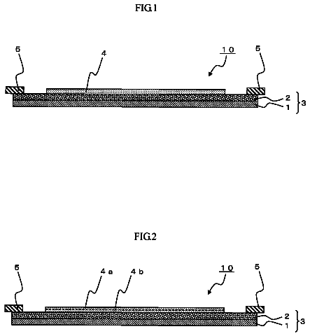
FIG. 1 is a schematic cross sectional view illustrating an example of an organic EL element.
FIG. 2 is a schematic constitutional drawing illustrating a production apparatus of an organic EL element according to one or more embodiments.
FIG. 3 is a schematic constitutional drawing illustrating an example of a film forming room constituting a production apparatus of an organic EL element.
FIG. 4 is a schematic drawing illustrating a part of a support substrate according to one or more embodiments.
FIG. 5A is a schematic side view illustrating a convey roller and a receive roller according to one or more embodiments.
FIG. 5B is a schematic side view illustrating a convey roller and a receive roller according to one or more embodiments.
FIG. 6A is a schematic drawing illustrating a part of continuous mask according to one or more embodiments.
FIG. 6B is a schematic drawing illustrating a part of continuous mask according to one or more embodiments.
FIG. 7 is a schematic constitutional drawing illustrating an example of a film forming room constituting a production apparatus of an organic EL element.
FIG. 8 is a schematic constitutional drawing illustrating an example of a film forming room constituting a production apparatus of an organic EL element.
FIG. 9A is a schematic drawing illustrating a part of continuous mask used in a film forming room of a hole injection layer according to one or more embodiments.
FIG. 9B is a schematic drawing illustrating a part of continuous mask used in a film forming room of a hole injection layer according to one or more embodiments.
FIG. 10 is a schematic constitutional drawing illustrating an example of a second patterning section.
FIG. 11 is a schematic drawing illustrating a part of continuous mask that is provided in a second patterning section according to one or more embodiments.
FIG. 12A is a schematic constitutional drawing illustrating an example of a second patterning section.
FIG. 12B is a schematic constitutional drawing illustrating an example of a second patterning section.
FIG. 13 is a schematic constitutional drawing illustrating a laminate room constituting a production apparatus of an organic EL element according to one or more embodiments.
FIG. 14 is a schematic drawing illustrating a part of back side film according to one or more embodiments.
FIG. 15 is a schematic drawing illustrating an example of an organic EL module.
FIG. 16 is a schematic cross sectional view illustrating an example of an organic EL element.
FIG. 17A is a plan view illustrating a pattern shape in a hole injection layer of a light emitting unit according to one or more embodiments.
FIG. 17AB is a plan view illustrating a pattern shape in a hole injection layer of a light emitting unit according to one or more embodiments.
FIG. 18 is a schematic drawing illustrating a schematic constitution of a mask used for light irradiation according to one or more embodiments.
A production method of an organic EL element of one or more embodiments of the present invention may be characterized in the following. At least one organic functional layer in each light emitting unit is patterned with a mask in the forming step of the organic functional layer, after formation of the organic functional layer, the organic functional layer is further patterned (patterning) by light irradiation so as to pattern into a region where a light emitting function is modulated, and a region where a light emitting function is not modulated. This feature is a common technical feature of one or more embodiments of the invention according to claim 1 to claim 7 .
In one or more embodiments of the present invention, it is preferable that the light irradiation in the second patterning step is done under conditions of: wavelength in the range of 320 to 420 nm; and radiation luminance in the range of 10 to 1,000 mW/cm.sup.2. By this, a specific light irradiation apparatus is not required in the production of an organic EL element. As a result, it can obtain an effect that an organic EL element according to one or more embodiments of the present invention may be easily produced.
Further, it is preferable that at least one of the organic functional layers patterned by light irradiation is a hole transport layer or a hole injection layer from the viewpoint of improving mask resolution.
A producing apparatus of an organic electroluminescent element according to one or more embodiments of the present invention is characterized in the following.
The producing apparatus contains:
a first patterning section to pattern with a mask at least one of the organic functional layers in each of the light emitting units; and
a second patterning section to pattern at least one of the organic functional layers by light irradiation into a region where a light emitting function is modulated, and a region where a light emitting function is not modulated,
wherein the second patterning section conducts the patterning each time when each of the light emitting units is produced.
Further, an organic EL element according to one or more embodiments of the present invention is appropriately provided in an organic EL module.
In one or more embodiments of the present invention, it is preferable that a polarizing member, a half mirror member, or a black filter is provided on a light emitting surface side of the support substrate.
Embodiments of the present invention and the constitution elements thereof, as well as configurations and embodiments to carry out embodiments of the present invention, will be detailed in the following. In the present description, when two figures are used to indicate a range of value before and after “to”, these figures are included in the range as a lowest limit value and an upper limit value.
<<Constitution of Organic EL Element>>
Preferable examples of a constitution of an organic EL element according to one or more embodiments of the present invention are described below. However, embodiments of the present invention are not limited to them. (I) Anode/first light emitting unit/intermediate electrode layer/second light emitting unit/cathode (II) Anode/first light emitting unit/first intermediate electrode layer/second light emitting unit/second intermediate electrode layer/third light emitting unit/cathode (I-1) Anode/white light emitting unit/intermediate electrode layer/white light emitting unit/cathode (II-1) Anode/white light emitting unit/first intermediate electrode layer/white light emitting unit/second intermediate electrode layer/white light emitting unit/cathode
As an example of an organic EL element according to one or more embodiments of the present invention, an organic EL element having the above-described constitution (I) is illustrated in FIG. 1 .
As illustrated in FIG. 1 , an organic EL element 1 is constituted by sequentially laminated on a support substrate 21 with an anode 23 , a first light emitting unit 25 a , an intermediate electrode layer 27 , a second light emitting unit 25 b , and a cathode 26 .
On a side edge portion of the support substrate 21 , the anode 4 is pulled out to form a taking-out wiring 24 that is formed in such a manner that a part thereof is in contact with the anode 23 . The intermediate electrode layer 27 has preferably a light transmitting property.
In one or more embodiments of the present invention, a sufficient number of light emitting units is 2 or more, and there is no limitation. However, by considering the production efficiency, a preferable number is in the range of 2 to 10, and a more preferable number is in the range of 2 to 3. Here, when a number of light emitting units is N (N is an integer of 2 or more), a number of intermediate metal layers is (N−1).
A light emitting unit in one or more embodiments of the present invention is a laminated body composed of one or a plurality of organic functional layers.
Examples of an organic functional layer used for a light emitting unit are known layers such as: a hole injection transport layer (an anode buffer layer), a hole transport layer, a light emitting layer, an electron transport layer, an electron injection layer (a cathode buffer layer), a hole blocking layer, and an electron blocking layer.
Preferable examples of a constitution and a lamination order of a light emitting unit are described below. However, embodiments of the present invention are not limited to them. (i) Hole injection transport layer/light emitting layer/electron injection transport layer (ii) Hole injection transport layer/light emitting layer/hole blocking layer/electron injection transport layer (iii) Hole injection transport layer/electron blocking layer/light emitting layer/hole blocking layer/electron injection transport layer (iv) Hole injection layer/hole transport layer/light emitting layer/electron transport layer/electron injection layer (v) Hole injection layer/hole transport layer/light emitting layer/hole blocking layer/electron transport layer/electron injection layer (vi) Hole injection layer/hole transport layer/electron blocking layer/light emitting layer/hole blocking layer/electron transport layer/electron injection layer
In one or more embodiments of the present invention, the light emitting units each may be composed of a different organic functional layer. However, it is preferable to be composed of the same organic functional layer and the same material. Further, it is preferable that the number of the light emitting layers is the same. By this, it can reduce the number of the employed substances for forming the light emitting units. This will produce a merit of cost and quality control. Moreover, it can improve production efficiency. And, when a vapor deposition process is employed for forming each organic functional layer, the film forming room can be commonly used for each light emitting unit. Thus, a merit of production efficiency will be benefited.
Each layer which constitutes a light emitting unit is formed with known thin film forming methods such as: a vapor deposition method, a spin coating method, a cast method, an LB (Langmuir-Blodgett method) method, an inkjet method, a spray method, a printing method, and a slot type coater method.
<<Production Method and Production Apparatus of Organic EL Element>>
In the following, a production method and a production apparatus of an organic EL element 1 are described by referring to FIG. 2 to FIG. 14 .
A production method of an organic EL element according to one or more embodiments of the present invention is a method of producing an organic EL element containing a support substrate having thereon: at least two light emitting units each containing one or a plurality of organic functional layers; and at least one intermediate electrode layer, the intermediate electrode layer being arranged between the light emitting units. The method is characterized in that it contains:
a first patterning step to pattern with a mask at least one of the organic functional layers in each of the light emitting units; and
a second patterning step to pattern the at least one of the organic functional layers by light irradiation into a region where a light emitting function is modulated, and a region where a light emitting function is not modulated,
wherein the second patterning step is conducted each time when each of the light emitting units is produced.
The production apparatus is not limited to a production apparatus 100 describe in the following.
In the production method of an organic EL element according to one or more embodiments of the present invention, it is preferable that the light irradiation in the second patterning step is done under conditions of: wavelength in the range of 320 to 420 nm; and radiation luminance in the range of 10 to 1,000 mW/cm.sup.2.
FIG. 2 is a schematic constitutional drawing illustrating a production apparatus 100 of an organic EL element according to one or more embodiments of the present invention. The production apparatus 100 indicated in FIG. 2 is an apparatus for producing an organic EL element 1 by continuously conveying a support substrate 21 wound in a roll condition. In addition, in one or more embodiments, a film forming surface of the support substrate 21 is provided with an inorganic insulating layer in advance. As an inorganic insulating layer, it may be suitably selected from the known compounds used in an organic EL element.
The support substrate 21 fed out from a feeding out section 101 placed under a reduced pressure enters an anterior room R 1 through guide rollers 102 and 103 . Further, it is conveyed in a surface treatment and accumulating room R 10 placed under a vacuum condition through a slit roller 104 , and dry cleaning of the surface and dewatering process are conducted. The pressure in the surface treatment and accumulating room R 10 is preferably set to be in the range of 1×10.sup.−5 to 10 Pa.
Subsequently, the support substrate 21 is continuously conveyed from the surface treatment and accumulating room R 10 to a film forming room R 20 . Between the surface treatment and accumulating room R 10 and the film forming room R 20 , there is provided with a gate valve or a pressure adjusting room. The difference of pressure between the surface treatment and accumulating room R 10 and the film forming room R 20 is adjusted.
In the production method according to one or more embodiments of the present invention, at first, a film forming process of any one of organic functional layers is conducted to the film forming surface of the conveying support substrate 21 in the film forming room R 20 and in a 6th film forming room R 30 described later.
Further, in this film forming process: a first patterning process is conducted to at least one of the organic functional layers in the light emitting unit by using a mask; and a second patterning process is conducted to make patterning by light irradiation into a region where a light emitting function is modulated, and a region where a light emitting function is not modulated.
In one or more embodiments, as a mask used for the first patterning process, a continuous mask, which will be described layer, is employed. The mask used for the first patterning process is not limited to the continuous mask, it may be used a known mask such as a plate mask.
In addition, the first patterning process is conducted in a first patterning section in which patterning is conducted to at least one of the organic functional layers in the light emitting unit by using a mask before formation of an intermediated electrode layer.
In one or more embodiments, a first patterning section designates a film forming room provided with a continuous mask among film forming rooms R 21 to R 25 described later. In the film forming room provided with a continuous mask, each organic functional layer is formed while patterning.
In one or more embodiments of the present invention, the first patterning section may be done to a plurality of organic functional layers, or to any one of organic functional layers. It is particularly preferable to be done to a hole transport layer or a hole injection layer.
The film forming room R 20 is constituted of a plurality of film forming rooms R 21 to R 25 and a second patterning section RL. Between the film forming rooms R 21 to R 25 and the second patterning section RL, there is provided with an accumulator mechanism which absorbs treatment speed. The film forming rooms R 21 to R 25 and the second patterning section RL each are independently vented to be kept in a vacuum condition or a reduced pressure condition. Although the film forming pressure depends of the film forming method, the film forming pressure is preferably set to be in the range of 1×10.sup.−6 to 10 Pa.
In the first film forming room R 21 , an anode 23 is formed on the support substrate 21 by using a film forming conductive material of a metal or a metal oxide with a film forming method such as a vacuum deposition method, a sputter method and an ion plating method.
Here, the first film forming room R 21 is described by referring to FIG. 3 . FIG. 3 is a schematic constitutional drawing of the first film forming room R 21 .
The first film forming room R 21 is constituted by containing inside with: a plurality of convey rollers 51 and 52 and receive rollers 53 and 54 conveying the support substrate 21 via a predetermined route, a raw material supplying section 55 facing the film forming surface of the support substrate 21 to be conveyed, and a back side cooling roller 56 to cool the support substrate 21 by contacting the opposite surface of the film forming surface of the support substrate 21 . Further, the inside of the first film forming room R 21 may be provided with: a continuous loop shape mask 60 having an opening section of a predetermined pattern shape, a rotate transport section 70 to rotate transport the continuous mask 60 in the loop direction, and a cleaning section 80 to make cleaning the continuous mask 60 .
Here, in one or more embodiments of the present invention, as indicated in FIG. 4 , the support substrate 21 has a plurality of first guide holes 211 having apertures with an equivalent interval at two edge portions of the width direction in the conveying direction (transport direction).
The convey rollers 51 and 52 have a plurality of projections located at the periphery in a diameter direction. During the conveying of the support substrate 21 , the projections are inserted in the first guide holes 211 of the support substrate 21 . By this, the support substrate 21 is smoothly conveyed. The convey rollers 51 and 52 are composed in the same manner as convey rollers 71 to 78 of the rotate transport section 70 that will be described later.
The receive roller 53 conveys the support substrate 21 together with convey rollers 51 and 52 by rotating driving. In addition, as indicated in FIG. 5A and FIG. 5B , the receive roller 53 is provided with a plurality of concave portions 530 on the surface thereof. The receive roller 54 is composed in the same manner as the receive roller 53 . These receive rollers 53 and 54 will be described in detail later.
The raw material supplying section 55 has a film forming mechanism corresponding to respective methods of a vacuum deposition method, a sputter method and an ion plating method. It is placed facing the film forming surface of the support substrate 21 . By this, an anode 23 is formed on the predetermined region of the film forming surface of the support substrate 21 that is conveyed in the first film forming room R 21 .
The back side cooling roller 56 is pivotably supported and it is a roller member that is provided with a predetermined cooling mechanism. The back side cooling roller 56 is placed in the opposite side of the raw material supplying section 55 across the support substrate 21 . Through contact with the opposite surface of the film forming surface of the support substrate 21 , it cools the film forming region of the support substrate 21 using by the raw material supplying section 55 .
The continuous mask 60 is a mask for continuous pattern forming. It is continuous in a loop form in the first film forming room R 21 . The continuous mask 60 is bridged with tension to a plurality of convey rollers 71 to 78 constituting the rotate transport section 70 .
The continuous mask 60 is described in the following by referring to FIG. 6A and FIG. 6A . FIG. 6A is a schematic drawing of the continuous mask 60 that is formed in a seamless state. FIG. 6B is a schematic drawing of the continuous mask 60 that is formed by bonding a plurality of sheet form masks 64 .
The continuous mask 60 has a plurality of opening section 61 having a predetermined pattern shape. Film formation is done on the support substrate 21 through this opening section 61 . Thus, it can form an anode having a predetermined pattern shape. Since the continuous mask 60 is closely contacted with the support substrate 21 being conveyed, it is preferable that the continuous mask 60 has flexibility in the same manner as the support substrate 21 .
Examples of a material for the continuous mask 60 are: Fe—Ni alloys such as SUS 300, invar, 42 alloy, Hastelloy™ and Inconel™; metal foils and alloy foils such as aluminum, magnesium, and titanium; thin plate ceramics and thin plate glass such as silicon, alumina and boronitride; thermoplastic resins such as polyester and polyurethane; and heat curable resins having high heat resistivity such as polyimide, epoxy resin, bakelite resin, polycarbonate, acrylic resin, urea resin, and phenol resin.
In particular, when a metal is used for a material of the continuous mask 60 , aperture forming is easily done, and the obtained continuous mask 60 has high thermal resistivity and low linear expansion coefficient. In addition, it can improve resistivity to the dry cleaning process that will be described later.
Moreover, when a heat curable resin is used for a material of the continuous mask 60 , it is preferable to include a glass fiber or a carbon fiber in the resin from the viewpoint of improving thermal resistivity and decreasing linear expansion coefficient. Thus, it is possible to improve size precision of the mask.
The thickness of the continuous mask 60 is preferably in the range of 0.1 to 3 mm from the viewpoint of flexibility and resistivity. Further, in order to give resistivity to the dry cleaning process and an easily peeling property from the adhered body, the surface of the continuous mask 60 may be treated with a Ni plating treatment, an alumite treatment, or a fluorine coating treatment.
As long as the continuous mask 60 is in the loop state, it may be formed in a seamless belt state having no bonding portion (refer to FIG. 6A ), or it may be formed with a plurality of sheet form masks, which are bonded together (refer to FIG. 6B ). When the continuous mask 60 is formed with a plurality of sheet form masks, the continuous mask 60 may be composed of a plurality of sheet form masks 64 by bonding them with bonding jigs 62 , the sheet form masks 64 being provided with an aperture area having a predetermined pattern beforehand, for example. As a bonding jig 62 , it may be used rivet fixing, metal chain bonding, flexible tape, and flexible belt. By the above-descried composition, the continuous mask 60 can be produced with a low cost, and even when a part of the continuous mask 60 is broken, the mask can be easily repaired and it can be reused by replacing only the broken sheet form masks.
Further, as indicated in FIG. 6A and FIG. 6B , the continuous mask 60 has a plurality of second guide holes 63 having apertures with an equivalent interval at two edge portions of the width direction in the loop direction (transport direction). The size of the plurality of second guide holes 63 and the interval are made to be the same size and interval as the first guide holes 211 of the support substrate 21 .
The rotate transport section 70 is composed of a plurality of convey rollers 71 to 78 . These convey rollers 71 to 78 are bridged with tension to the continuous mask 60 . Through rotating driving of the plurality of convey rollers 71 to 78 , the continuous mask 60 will be rotate transported to the moving direction of the loop. The rotate transport section 70 can make overlap a part of the continuous mask 60 with the support substrate 21 being conveyed by rotate transporting the continuous mask 60 . Moreover, the rotate transport section 70 can detach the continuous mask 60 overlapped with the support substrate 21 by further rotate transporting the continuous mask 60 .
In addition, the rotate transporting speed of the continuous mask 60 by the rotate transport section 70 is controlled to be the same as the transport speed of the support substrate 21 .
The convey roller 71 is described by referring to FIG. 5A and FIG. 5B . FIG. 5A is a drawing of the convey roller 71 and receive roller 53 viewed from the axis direction. FIG. 5B is a side view of the convey roller 71 and receive roller 53 .
As indicated in FIG. 5A and FIG. 5B , the convey roller 71 is composed of: a rotating shaft 711 capable of rotate driving; a roller 712 placed in the center portion of the shaft direction of the rotating shaft 711 ; and rollers 713 and 714 placed at the both edges of the rotating shaft 711 . The roller 712 is fixed to the rotating shaft 711 , and it rotates with the rotating driving of the rotating shaft 71 . The rollers 713 and 714 are fixed to the rotating direction of the rotating shaft 711 , and they are placed in a state movable to the separating direction with respect to the shaft direction of the rotating shaft 711 with each other (an arrow direction in FIG. 5B ). The rollers 713 and 714 are respectively provided with a plurality of projections 715 located at the periphery in a diameter direction. The projections 715 of the rollers 713 and 714 are inserted in the second guide holes 63 of the continuous mask 60 , thereby the convey roller 71 can smoothly rotate transport the continuous mask 60 . In addition, tension of the width direction can be given to the continuous mask 60 by making to move the rollers 713 and 714 to a separating direction with each other during the condition of inserting the projections 715 of the rollers 713 and 714 into the second guide holes 63 . By this, the continuous mask 60 can be overlapped to the support substrate 21 with high precision. It is preferable that the projections 715 are formed in a tapered shape to be easily inserted in the second guide holes 63 . The convey rollers 72 to 78 are composed in the same manner as the convey roller 71 .
Among the convey rollers 71 to 78 , the convey rollers 71 and 74 are located to be contact with the receive rollers 53 and 54 . The projections 715 of the convey roller 71 are made to be contained in the concave portions 530 of the receive roller 53 . As a result, the convey rollers 71 and 74 are contacted with the receive rollers 53 and 54 without space. By this, the continuous mask 60 rotate transported by the convey rollers 71 and 74 will be overlapped to the support substrate 21 conveyed by the receive rollers 53 and 54 to result in achieving close contact condition.
The projections 715 of the convey rollers 71 and 74 are inserted in the second guide holes 63 of the continuous mask 60 , and at the same time, they are inserted in the first guide holes 211 of the support substrate 21 . Since the first guide holes 211 and the second guide holes 63 are formed in a corresponding position with each other, it can overlap the continuous mask 60 and the support substrate 21 with making alignment by inserting the projections 715 in the first guide holes 211 and the second guide holes 63 . Consequently, alignment of high precision and patterning film formation can be made while conveying the support substrate 21 without using a complex alignment mechanism.
In addition, by the mechanism of moving the rollers 713 and 714 of the convey rollers 71 and 74 to the separating direction with each other, tension to the width direction can be given not only to the continuous mask 60 but to the support substrate 21 .
The description continues in the full USPTO document.
 Lapsed, fee not paid1 drawing