 Lapsed, fee not paid11 drawings
Software & Apps · US 9,753,638 B2
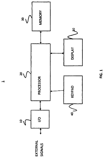
Method and apparatus for entering symbols from a touch-sensitive screen
A method enables a user to enter symbols into an entry field from a touch-sensitive screen.
US 9,753,653 B2 · Assignee: SanDisk Technologies LLC · Inventors: Ellis; Robert W. et al.
Sheet 1 of 9 from the published document. All sheets in the USPTO PDF
Systems, methods, and/or devices are used to manage high-priority NAND operations. In some embodiments, the method includes receiving a first command (e.g., requesting a high-priority memory operation) corresponding to a first location (e.g., having both a first physical address and a first aliased physical address) in a first die of a plurality of physical non-volatile memory die in a storage device. If the first die is performing a blocking low-priority memory operation (e.g., the low-priority operation was sent to the first die using a second physical address), the method includes sending a memory operation command, corresponding to the first memory operation, to the first die using the first aliased physical address. In some embodiments, a predefined die-selection portion of the second physical address matches the predefined die-selection portion of the first physical address and does not match the predefined die-selection portion of the first aliased physical address.
Semiconductor memory devices, including flash memory, typically utilize memory cells to store data as an electrical value, such as an electrical charge or voltage. A flash memory cell, for example, includes a single transistor with a floating gate that is used to store a charge representative of a data value. Flash memory is a non-volatile data storage device that can be electrically erased and reprogrammed. More generally, non-volatile memory (e.g., flash memory, as well as other types of non-volatile memory implemented using any of a variety of technologies) retains stored information even without power, as opposed to volatile memory, which requires power to maintain the stored information. State machines are, in some embodiments, used in a storage controller of a non-volatile memory device (e.g., comprising a plurality of physical non-volatile memory die) to help manage command proces
8 of 9 drawing sheets so far from the published document, cropped to the drawing. Every sheet is in the USPTO PDF.
What the patent claimed, word for word. All of it is now free to use.
The disclosed embodiments relate generally to command processing in a storage device (e.g., a device including one or more flash memory devices), and in particular, to managing high-priority NAND operations in storage devices.
Semiconductor memory devices, including flash memory, typically utilize memory cells to store data as an electrical value, such as an electrical charge or voltage. A flash memory cell, for example, includes a single transistor with a floating gate that is used to store a charge representative of a data value. Flash memory is a non-volatile data storage device that can be electrically erased and reprogrammed. More generally, non-volatile memory (e.g., flash memory, as well as other types of non-volatile memory implemented using any of a variety of technologies) retains stored information even without power, as opposed to volatile memory, which requires power to maintain the stored information.
State machines are, in some embodiments, used in a storage controller of a non-volatile memory device (e.g., comprising a plurality of physical non-volatile memory die) to help manage command processing. After receiving a command, the state machine determines whether a location on a non-volatile memory die corresponding to the received command is busy (e.g., currently executing a memory operation). If the location is busy, then the non-volatile memory device waits and sends the command (or a memory operation corresponding to the command) when the location is no longer busy. Therefore, in such embodiments, a non-volatile memory device may permit a slow low-priority operation (e.g., a write operation) to complete execution before beginning execution of a higher-priority fast operation (e.g., a read operation requested by a host device), resulting in a waste of computing resources and causing non-volatile memory devices to violate quality of service metrics (i.e., performance-based warranties) associated with a maximum latency for commands sent by a host system.
Without limiting the scope of the appended claims, after considering this disclosure, and particularly after considering the section entitled “Detailed Description” one will understand how the aspects of various embodiments are implemented and used to improve command executions times by intelligently managing high-priority NAND operations. In some embodiments, a storage device that includes a plurality of physical non-volatile memory die receives a request to perform a high-priority memory operation at a first location in a first die of the plurality of physical non-volatile memory die. The first location, in some embodiments, has both a first physical address and a first aliased physical address distinct from the first physical address. In accordance with a determination that the first die is performing a blocking low-priority memory operation (e.g., the low-priority memory operation was sent to the first die using a second physical address), the storage device sends the high-priority memory operation to the first die using the first aliased physical address. In some embodiments, a predefined die-selection portion of the second physical address matches the predefined die-selection portion of the first physical address and does not match the predefined die-selection portion of the first aliased physical address.
So that the present disclosure can be understood in greater detail, a more particular description may be had by reference to the features of various embodiments, some of which are illustrated in the appended drawings. The appended drawings, however, merely illustrate pertinent features of the present disclosure and are therefore not to be considered limiting, for the description may admit to other effective features.
FIGS. 1A and 1B are block diagrams illustrating implementations of a data storage system in accordance with some embodiments.
FIGS. 2A and 2B are block diagrams illustrating implementations of management modules in accordance with some embodiments.
FIG. 3A is a block diagram illustrating status monitoring data structures and, more specifically, a status table for managing high-priority operations, in accordance with some embodiments.
FIG. 3B is a block diagram illustrating memory operation commands.
FIG. 4 illustrates a flowchart representation of a method of managing high-priority operations in a storage device in accordance with some embodiments.
FIGS. 5A-5C illustrate flowchart representations of methods of managing high-priority operations in a storage device, in accordance with some embodiments.
In accordance with common practice, the various features illustrated in the drawings may not be drawn to scale. Accordingly, the dimensions of the various features may be arbitrarily expanded or reduced for clarity. In addition, some of the drawings may not depict all of the components of a given system, method or device. Finally, like reference numerals may be used to denote like features throughout the specification and figures.
When a storage device (e.g., a non-volatile memory device having a plurality of physical non-volatile memory die) is unable to send a command to a non-volatile memory die that is currently executing a blocking low-priority operation (e.g., because a state machine of a storage controller of the storage device indicates that the die, or a required portion of the die, is busy), violations of quality of service metrics can occur (e.g., because commands with quality of service metrics requiring fast execution times have to wait on slow commands, thereby making it difficult to meet the quality of service metric). Consequently, what is desired are mechanisms for managing high-priority NAND operations, in order to ensure that high-priority commands are executed quickly and do not need to wait for completed execution of low-priority commands.
The various embodiments described herein include systems, methods, and/or devices used to manage high-priority operations in a storage device. Some embodiments include systems, methods and/or devices to send high-priority memory operations to a non-volatile memory die using an aliased address for the non-volatile memory die, while the non-volatile memory die is executing a low-priority operation.
(A1) More specifically, some embodiments include a method of managing a storage device that includes a plurality of physical non-volatile memory die. In some embodiments, the method includes receiving at the storage device a first command corresponding to a first location in a first die of the plurality of physical non-volatile memory die in the storage device. The first command, in some embodiments or circumstances, requests a first memory operation including a high-priority operation and the first location has both a first physical address and a first aliased physical address distinct from the first physical address. In accordance with a determination that the first die is performing a blocking low-priority memory operation, the method further includes: sending a memory operation command, corresponding to the first memory operation, to the first die using the first aliased physical address. In some embodiments or circumstances, the blocking low-priority operation was sent to the first die using a second physical address. A predefined die-selection portion of the second physical address, in some embodiments, matches the predefined die-selection portion of the first physical address and does not match the predefined die-selection portion of the first aliased physical address.
(A2) In some embodiments of the method of A1, the method further includes: in response to receiving the first command, determining whether the first die is performing a blocking low-priority memory operation.
(A3) In some embodiments of the method of any one of A1 to A2, a predefined intra-die portion of the first physical address matches the predefined intra-die portion of the first aliased physical address, and the predefined die-selection portion of the first physical address does not match the predefined die-selection portion of the first aliased physical address.
(A4) In some embodiments of the method of any one of A1 to A3, the method further includes: at the first die, in response to receiving the memory operation command corresponding to the first memory operation, suspending performance of the blocking low-priority memory operation. After the suspending, the method further includes performing the first memory operation. After performing the first memory operation, the method further includes resuming performance of the blocking low-priority memory operation.
(A5) In some embodiments of the method of any one of A1 to A3, the method further includes, at the first die, in response to receiving the memory operation command corresponding to the first memory operation, suspending performance of the blocking low-priority memory operation. After the suspending, the method further includes performing the first memory operation. After performing the first memory operation and in accordance with a determination that the suspended blocking low-priority memory operation is not yet complete, the method further includes resuming performance of the blocking low-priority memory operation.
(A6) In some embodiments of the method of any of any one of A4 or A5, suspending performance of the blocking low-priority memory operation includes the first die automatically suspending performance of the blocking low-priority memory operation after receiving the memory operation command corresponding to the first memory operation.
(A7) In some embodiments of the method of any one of A4 to A6, the method further includes: after the suspending and prior to the resuming, performing the first memory operation and another memory operation including a second high-priority memory operation.
(A8) In some embodiments of the method of any one of A1 to A3, performance of the blocking low-priority memory operation includes execution of a sequence of segmented memory operations. In some embodiments, the method further includes: in response to receiving the memory operation command corresponding to the first memory operation, suspending performance of the blocking low-priority memory operation upon completion of a respective segment of the sequence of segmented memory operations. After the suspending, the method further includes performing the first memory operation. After performing the first memory operation, the method further includes resuming performance of the blocking low-priority memory operation by performing a next segment of the sequence of segmented memory operations.
(A9) In some embodiments of the method of A8, the first command is received at a storage controller of the storage device, the suspending and resuming performance of the blocking low-priority memory operation is performed by a local controller in a module having two or more die of the plurality of physical die, and the local controller is distinct from the storage controller of the storage device.
(A10) In some embodiments of the method of any one of A1 to A9, the first command requests a read operation.
(A11) In some embodiments of the method of A10, the method further includes: sending a second memory operation command, corresponding to a low-priority read operation, to the first die using a physical address having a predefined die-selection portion that matches the predefined die-selection portion of the second physical address.
(A12) In some embodiments of the method of any one of A1 to A11, the blocking low-priority memory operation is an erase operation or a write operation.
(A13) In another aspect, a storage device includes non-volatile memory (e.g., one or more non-volatile storage devices, such as flash memory devices), one or more processors, and a storage controller having one or more controller modules configured to receive at the storage device a first command corresponding to a first location in a first die of the plurality of physical non-volatile memory die in the storage device. The first command, in some embodiments or circumstances, requests a first memory operation including a high-priority operation and the first location has both a first physical address and a first aliased physical address distinct from the first physical address. The one or more controller modules are further configured to send, in accordance with a determination that the first die is performing a blocking low-priority memory operation, a memory operation command, corresponding to the first memory operation, to the first die using the first aliased physical address. The blocking low-priority operation, in some embodiments, was sent to the first die using a second physical address, a predefined die-selection portion of which matches the predefined die-selection portion of the first physical address and does not match the predefined die-selection portion of the first aliased physical address.
(A14) In some embodiments of the storage device of A13, the one or more controller modules include: 1) a status monitoring module to determine whether the first die is performing a blocking low-priority memory operation; and 2) a command processing module to receive at the storage device the first command and to send, in accordance with the determination that the first die is performing a blocking low-priority memory operation, the memory operation command corresponding to the first memory operation to the first die using the first aliased physical address.
(A15) In some embodiments of the storage device of A14, the storage device further includes a plurality of storage modules, each storage module including: 1) a local controller including an instance of the command processing module and an instance of the status monitoring module; and 2) a plurality of non-volatile memory devices. In some embodiments or circumstances, the first command is for reading data from a first storage module of the plurality of storage modules, and the first storage module includes the first die. The instance of the status monitoring module in the first storage module is configured, in some embodiments, to determine whether the first die is performing a blocking low-priority memory operation.
(A16) In some embodiments of the storage device of any one of A13 to A14, the storage device further includes a plurality of storage modules, each storage module having a local controller and a plurality of non-volatile memory devices.
(A17) In some embodiments of the storage device of any one of A13 to A16, the one or more controller modules are further configured to perform the method of any one of A2 to A12 described above.
(A18) In yet another aspect, a storage device includes non-volatile memory, one or more processors, and means for performing of the method of any one of A1 to A12 described above.
(A19) In yet another aspect, a non-transitory computer-readable storage medium stores one or more programs configured for execution by one or more processors of a storage device, the one or more programs including instructions for causing the storage device to perform the method of any one of A1 to A12 described above.
Numerous details are described herein in order to provide a thorough understanding of the example embodiments illustrated in the accompanying drawings. However, some embodiments may be practiced without many of the specific details, and the scope of the claims is only limited by those features and aspects specifically recited in the claims. Furthermore, well-known methods, components, and circuits have not been described in exhaustive detail so as not to unnecessarily obscure pertinent aspects of the embodiments described herein.
FIG. 1A is a block diagram illustrating an implementation of a data storage system 100 , in accordance with some embodiments. While some example features are illustrated, various other features have not been illustrated for the sake of brevity and so as not to obscure pertinent aspects of the example embodiments disclosed herein. To that end, as a non-limiting example, data storage system 100 includes a storage device 120 (also sometimes called an information storage device, or a data storage device, or a memory device), which includes a storage controller 124 and a storage medium 132 , and is used in conjunction with or includes a computer system 110 (e.g., a host system or a host computer). In some embodiments, storage medium 132 is a single flash memory device while in other embodiments storage medium 132 includes a plurality of flash memory devices. In some embodiments, storage medium 132 is NAND-type flash memory or NOR-type flash memory. In some embodiments, storage medium 132 includes one or more three-dimensional (3D) memory devices. Further, in some embodiments, storage controller 124 is a solid-state drive (SSD) controller. However, other types of storage media may be included in accordance with aspects of a wide variety of embodiments (e.g., PCRAM, ReRAM, STT-RAM, etc.). In some embodiments, a flash memory device includes one or more flash memory die, one or more flash memory packages, one or more flash memory channels or the like. In some embodiments, data storage system 100 can contain one or more storage devices 120 .
Computer system 110 is coupled to storage controller 124 through data connections 101 . However, in some embodiments computer system 110 includes storage controller 124 , or a portion of storage controller 124 , as a component and/or as a subsystem. For example, in some embodiments, some or all of the functionality of storage controller 124 is implemented by software executed on computer system 110 . Computer system 110 may be any suitable computer device, such as a computer, a laptop computer, a tablet device, a netbook, an internet kiosk, a personal digital assistant, a mobile phone, a smart phone, a gaming device, a computer server, or any other computing device. Computer system 110 is sometimes called a host, host system, client, or client system. In some embodiments, computer system 110 is a server system, such as a server system in a data center. In some embodiments, computer system 110 includes one or more processors, one or more types of memory, a display and/or other user interface components such as a keyboard, a touch-screen display, a mouse, a track-pad, a digital camera, and/or any number of supplemental I/O devices to add functionality to computer system 110 . In some embodiments, computer system 110 does not have a display and other user interface components.
Storage medium 132 is coupled to storage controller 124 through connections 103 . Connections 103 are sometimes called data connections, but typically convey commands in addition to data, and optionally convey metadata, error correction information and/or other information in addition to data values to be stored in storage medium 132 and data values read from storage medium 132 . In some embodiments, however, storage controller 124 and storage medium 132 are included in the same device (i.e., an integrated device) as components thereof. Furthermore, in some embodiments, storage controller 124 and storage medium 132 are embedded in a host device (e.g., computer system 110 ), such as a mobile device, tablet, other computer or computer controlled device, and the methods described herein are performed, at least in part, by the embedded storage controller. Storage medium 132 may include any number (i.e., one or more) of memory devices including, without limitation, non-volatile semiconductor memory devices, such as flash memory device(s). For example, flash memory device(s) can be configured for enterprise storage suitable for applications such as cloud computing, for database applications, primary and/or secondary storage, or for caching data stored (or to be stored) in secondary storage, such as hard disk drives. Additionally and/or alternatively, flash memory device(s) can also be configured for relatively smaller-scale applications such as personal flash drives or hard-disk replacements for personal, laptop, and tablet computers.
Storage medium 132 is divided into a number of addressable and individually selectable blocks, such as selectable portion 133 . In some embodiments, the individually selectable blocks are the minimum size erasable units in a flash memory device. In other words, each block contains the minimum number of memory cells that can be erased without erasing any other memory cells in the same flash memory device. Typically, when a flash memory block is erased, all memory cells in the block are erased simultaneously. Each block is usually further divided into a plurality of pages and/or word lines, where each page or word line is typically an instance of the smallest individually accessible (readable) portion in a block. In some embodiments (e.g., using some types of flash memory), the smallest individually accessible unit of a data set, however, is a sector, which is a subunit of a page. That is, a block includes a plurality of pages, each page contains a plurality of sectors, and each sector is the minimum unit of data for reading data from the flash memory device. For example, in some implementations, each block includes a number of pages, such as 64 pages, 128 pages, 256 pages or another suitable number of pages. Blocks are typically grouped into a plurality of zones. Each block zone can be independently managed to some extent, which increases the degree of parallelism for parallel operations and simplifies management of storage medium 132 .
Additionally, if data is written to a storage medium in pages, but the storage medium is erased in blocks, pages in the storage medium may contain invalid (e.g., stale) data, but those pages cannot be overwritten until the whole block containing those pages is erased. In order to write to the pages with invalid data, the pages (if any) with valid data in that block are read and re-written to a new block and the old block is erased (or put on a queue for erasing). This process is called garbage collection. After garbage collection, the new block contains the pages with valid data and may have free pages that are available for new data to be written, and the old block can be erased so as to be available for new data to be written. Since flash memory can only be programmed and erased a limited number of times, the efficiency of the algorithm used to pick the next block(s) to re-write and erase has a significant impact on the lifetime and reliability of flash-based storage systems.
Another phenomenon that impacts the lifetime and reliability of flash-based storage systems (in some embodiments, storage medium 132 ) is write amplification. Write amplification is a phenomenon where the actual amount of physical data written to a storage medium (e.g., NVM devices 140 , 142 in storage device 120 ) is a multiple of the logical amount of data written by a host (e.g., computer system 110 , sometimes called a host) to the storage medium. As discussed above, when a block of storage medium must be erased before it can be re-written, the garbage collection process to perform these operations results in re-writing data one or more times. This multiplying effect increases the number of writes required over the life of a storage medium, which shortens the time it can reliably operate. The formula to calculate the write amplification of a storage system is given by equation:
amount of data written to a storage medium amount of data written by a host
One of the goals of any flash memory based data storage system architecture is to reduce write amplification as much as possible so that available endurance is used to meet storage medium reliability and warranty specifications. Higher system endurance also results in lower cost as the storage system may need less over-provisioning, where over-provisioning is storage capacity in a storage device or system that is in excess of the declared capacity of the storage device or system. By reducing write amplification, the endurance of the storage medium is increased and the overall cost of the storage system is decreased. Generally, garbage collection is performed on erase blocks with the fewest number of valid pages for best performance and best write amplification.
Continuing with the description of FIG. 1A , in some embodiments, storage controller 124 includes a management module 121 - 1 , a host interface 129 , a storage medium (I/O) interface 128 , and additional module(s) 125 . Storage controller 124 may include various additional features that have not been illustrated for the sake of brevity and so as not to obscure pertinent features of the example embodiments disclosed herein, and a different arrangement of features may be possible.
Host interface 129 provides an interface to computer system 110 through data connections 101 . Similarly, storage medium interface 128 provides an interface to storage medium 132 though connections 103 . In some embodiments, storage medium interface 128 includes read and write circuitry, including circuitry capable of providing reading signals to storage medium 132 (e.g., reading threshold voltages for NAND-type flash memory, as discussed below). In some embodiments, connections 101 and connections 103 are implemented as a communication media over which commands and data are communicated, using a protocol such as DDR3, SCSI, SATA, SAS, or the like. In some embodiments, storage controller 124 includes one or more processing units (also sometimes called CPUs, processors, microprocessors, or microcontrollers) configured to execute instructions in one or more programs (e.g., in storage controller 124 ). In some embodiments, the one or more processors are shared by one or more components within, and in some cases, beyond the function of storage controller 124 .
In some embodiments, management module 121 - 1 includes one or more central processing units (CPUs, also sometimes called processors, microprocessors or microcontrollers) 122 configured to execute instructions in one or more programs (e.g., in management module 121 - 1 ). In some embodiments, the one or more CPUs 122 are shared by one or more components within, and in some cases, beyond the function of storage controller 124 . Management module 121 - 1 is coupled to host interface 129 , additional module(s) 125 and storage medium interface 128 in order to coordinate the operation of these components. In some embodiments, one or more modules of management module 121 - 1 are implemented in management module 121 - 2 of computer system 110 . In some embodiments, one or more processors of computer system 110 (not shown) are configured to execute instructions in one or more programs (e.g., in management module 121 - 2 ). Management module 121 - 2 is coupled to storage device 120 in order to manage the operation of storage device 120 .
Additional module(s) 125 are coupled to storage medium interface 128 , host interface 129 , and management module 121 - 1 . As an example, additional module(s) 125 may include an error control module to limit the number of uncorrectable errors inadvertently introduced into data during writes to memory and/or reads from memory. In some embodiments, additional module(s) 125 are executed in software by the one or more CPUs 122 of management module 121 - 1 , and, in other embodiments, additional module(s) 125 are implemented in whole or in part using special purpose circuitry (e.g., to perform encoding and decoding functions). In some embodiments, additional module(s) 125 are implemented in whole or in part by software executed on computer system 110 .
As data storage densities of non-volatile semiconductor memory devices continue to increase, stored data is more prone to being stored and/or read erroneously. In some embodiments, error control coding can be utilized to limit the number of uncorrectable errors that are introduced by electrical fluctuations, defects in the storage medium, operating conditions, device history, write-read circuitry, etc., or a combination of these and various other factors.
In some embodiments, an error control module, included in additional module(s) 125 , includes an encoder and a decoder. In some embodiments, the encoder encodes data by applying an error control code (ECC) to produce a codeword, which is subsequently stored in storage medium 132 . When encoded data (e.g., one or more codewords) is read from storage medium 132 , the decoder applies a decoding process to the encoded data to recover the data, and to correct errors in the recovered data within the error correcting capability of the error control code. Those skilled in the art will appreciate that various error control codes have different error detection and correction capacities, and that particular codes are selected for various applications for reasons beyond the scope of this disclosure. As such, an exhaustive review of the various types of error control codes is not provided herein. Moreover, those skilled in the art will appreciate that each type or family of error control codes may have encoding and decoding algorithms that are particular to the type or family of error control codes. On the other hand, some algorithms may be utilized at least to some extent in the decoding of a number of different types or families of error control codes. As such, for the sake of brevity, an exhaustive description of the various types of encoding and decoding algorithms generally available and known to those skilled in the art is not provided herein.
In some embodiments, during a write operation, host interface 129 receives data to be stored in storage medium 132 from computer system 110 . The data received by host interface 129 is made available to an encoder (e.g., in additional module(s) 125 ), which encodes the data to produce one or more codewords. The one or more codewords are made available to storage medium interface 128 , which transfers the one or more codewords to storage medium 132 in a manner dependent on the type of storage medium being utilized.
In some embodiments, a read operation is initiated when computer system (host) 110 sends one or more host read commands (e.g., via data connections 101 , or alternatively a separate control line or bus) to storage controller 124 requesting data from storage medium 132 . Storage controller 124 sends one or more read access commands to storage medium 132 , via storage medium interface 128 , to obtain raw read data in accordance with memory locations (or logical addresses, object identifiers, or the like) specified by the one or more host read commands. Storage medium interface 128 provides the raw read data (e.g., comprising one or more codewords) to a decoder (e.g., in additional module(s) 125 ). If the decoding is successful, the decoded data is provided to host interface 129 , where the decoded data is made available to computer system 110 . In some embodiments, if the decoding is not successful, storage controller 124 may resort to a number of remedial actions or provide an indication of an irresolvable error condition.
As explained above, a storage medium (e.g., NVM devices 140 , 142 ) is divided into a number of addressable and individually selectable blocks and each block is optionally (but typically) further divided into a plurality of pages and/or word lines and/or sectors. While erasure of a storage medium is performed on a block basis, in many embodiments, reading and programming of the storage medium is performed on a smaller subunit of a block (e.g., on a page basis, word line basis, or sector basis). In some embodiments, the smaller subunit of a block consists of multiple memory cells (e.g., single-level cells or multi-level cells). In some embodiments, programming is performed on an entire page. In some embodiments, a multi-level cell (MLC) NAND flash typically has four possible states per cell, yielding two bits of information per cell. Further, in some embodiments, a MLC NAND has two page types:
a lower page (sometimes called fast page), and
an upper page (sometimes called slow page). In some embodiments, a triple-level cell (TLC) NAND flash has eight possible states per cell, yielding three bits of information per cell. Although the description herein uses TLC, MLC, and SLC as examples, those skilled in the art will appreciate that the embodiments described herein may be extended to memory cells that have more than eight possible states per cell, yielding more than three bits of information per cell. In some embodiments, the encoding format of the storage media (i.e., TLC, MLC, or SLC and/or a chosen data redundancy mechanism) is a choice made (or implemented) when data is actually written to the storage media.
In some embodiments, the memory die (e.g., NVM devices 140 , 142 ) can handle only one memory operation (e.g., read, write or erase) at a time, but in other embodiments, the memory die are so-called multi-plane devices that can execute, in parallel, one command per plane. Typically, such memory die have two planes, and can execute two commands in parallel. But in other embodiments, such memory die may have N planes, where N is greater than 2, and can execute N memory commands in parallel. When a currently executing memory command and/or a previously enqueued memory command awaiting execution is directed to the same die and plane as a newly received memory command, sending the newly received memory command to the memory die must be delayed, absent some form of intervention, until the currently executing memory command and/or any previously enqueued memory command awaiting execution by the same memory die and plane have completed execution.
A “blocking low-priority memory operation” is thus a previously received memory operation (A) that requires the same resources (e.g., the same memory die, in the case of a single-plane memory die, or the same memory die and plane in the case of a multi-plan memory die) as a currently received or newly received memory operation command, and (B) that has not yet completed execution.
Flash memory devices (in some embodiments, storage medium 132 ) utilize memory cells (e.g., SLC, MLC, and/or TLC) to store data as electrical values, such as electrical charges or voltages. Each flash memory cell typically includes a single transistor with a floating gate that is used to store a charge, which modifies the threshold voltage of the transistor (i.e., the voltage needed to turn the transistor on). The magnitude of the charge, and the corresponding threshold voltage the charge creates, is used to represent one or more data values. In some embodiments, during a read operation, a reading threshold voltage is applied to the control gate of the transistor and the resulting sensed current or voltage is mapped to a data value.
The terms “cell voltage” and “memory cell voltage,” in the context of flash memory cells, mean the threshold voltage of the memory cell, which is the minimum voltage that needs to be applied to the gate of the memory cell's transistor in order for the transistor to conduct current. Similarly, reading threshold voltages (sometimes also called reading signals and reading voltages) applied to flash memory cells are gate voltages applied to the gates of the flash memory cells to determine whether the memory cells conduct current at that gate voltage. In some embodiments, when a flash memory cell's transistor conducts current at a given reading threshold voltage, indicating that the cell voltage is less than the reading threshold voltage, the raw data value for that read operation is a “1” and otherwise the raw data value is a “0.”
Attention is now directed to FIG. 1B , illustrating a block diagram of an implementation of a data storage system 100 , in accordance with some embodiments. To avoid needless repetition of explanations already provided above, features and components of data storage system 100 already shown in FIG. 1A and described above, and shown again in FIG. 1B , are not described again here, and instead only additional features and components are described with respect to FIG. 1B . Additionally, some components illustrated in FIG. 1A are, in some embodiments, still a part of the implementation illustrated in FIG. 1B , although not explicitly illustrated. For example, NVM Modules 160 , in some embodiments are included as components of storage medium 132 ( FIG. 1A ). As such, the features and components of storage medium 132 , described above with respect to in FIG. 1A , are in some embodiments also applicable to NVM devices 140 , 142 contained within NVM Modules 160 . In some embodiments in which data storage system 100 includes a plurality of storage devices 120 , one or more of the storage devices are configured as illustrated in FIG. 1B , while other storage devices are configured as illustrated in FIG. 1A .
As a non-limiting example, data storage system 100 includes storage device 120 , which includes one or more NVM modules (e.g., NVM modules(s) 160 ). Each NVM module 160 includes one or more NVM module controllers (e.g., NVM module controllers 130 - 1 through 130 -m), and one or more NVM devices (e.g., one or more NVM device(s) 140 , 142 ).
In this non-limiting example, data storage system 100 is used in conjunction with computer system 110 . In some implementations, storage device 120 includes a single NVM device while in other implementations storage device 120 includes a plurality of NVM devices. In some implementations, NVM devices 140 , 142 include NAND-type flash memory or NOR-type flash memory. Further, in some implementations, each NVM module controller 130 is or includes a solid-state drive (SSD) controller. However, one or more other types of storage media may be included in accordance with aspects of a wide variety of implementations.
In some embodiments, the one or more NVM controllers 130 are coupled with storage controller 124 through connections 103 . Connections 103 are sometimes called data connections, but typically convey commands in addition to data, and optionally convey metadata, error correction information, and/or other information in addition to data values to be stored in NVM devices 140 , 142 and data values read from NVM devices 140 , 142 . In some embodiments, however, storage controller 124 , the one or more NVM controllers 130 , and NVM devices 140 , 142 are included in the same device (i.e., an integrated device such as storage medium 132 of FIG. 1A ) as components thereof. Furthermore, in some embodiments, storage controller 124 , is embedded in a host device (e.g., computer system 110 ), such as a mobile device, tablet, other computer or computer controlled device, and the methods described herein are performed, at least in part, by the embedded storage controller.
In some embodiments, one or more NVM modules 160 include NVM devices 140 , 142 such as flash memory devices (e.g., NVM devices 140 - 1 through 140 -n, and NVM devices 142 - 1 through 142 -k) and NVM controllers 130 (e.g., NVM controllers 130 - 1 through 130 -m). Viewed another way, storage device 120 includes m memory channels, each of which has an NVM controller 130 and a set of NVM devices 140 or 142 coupled to the NVM controller 130 , where m is an integer greater than one. However, in some embodiments, two or more memory channels share an NVM controller 130 . In either example, each memory channel has its own distinct set of NVM devices 140 or 142 . In a non-limiting example, the number of memory channels in a typical NVM module is 8, 16 or 32. In another non-limiting example, the number of NVM devices 140 or 142 per memory channel is typically 8, 16, 32 or 64. Furthermore, in some embodiments, the number of NVM devices 140 / 142 is different in different memory channels.
The description continues in the full USPTO document.
About 6,397 words. The USPTO PDF has it with every drawing.
Fees are due 3.5, 7.5 and 11.5 years after grant. This patent expired on September 5, 2025, so the fee marked "not paid" was the one that went unpaid.
High-Priority NAND Operations Management
Filed Oct 2015 · published Oct 2016High-priority NAND operations management
Filed Oct 2015 · granted Sep 2017Earlier publications, parents and continuations. None of them can still be enforced, or this patent would not be listed.
Prior art cited by the examiner or applicant. Useful when you check your own idea for novelty.
Everything on this page comes from the documents linked above.


