Background of the invention
Field of the Invention
The present invention relates to a color filter substrate, a liquid crystal display device, and a method for manufacturing a color filter substrate.
This application is based on and claims priority from earlier Japanese Patent Application No. 2013-012006 filed Jan. 25, 2013, the description of which is incorporated herein by reference.
Discussion of the Background
Liquid crystal panels provided to generally used liquid crystal display devices have a configuration in which a liquid crystal layer is sandwiched between two substrates. For example, the two substrates each include a transparent substrate made such as of glass. Such a liquid crystal panel has a front side and a back side each of which is provided with a polarizing plate, or a polarizing plate and a retardation plate.
An organic electroluminescence display device (hereinafter referred to as organic EL display device) includes a white light-emitting organic EL in place of liquid crystal. The organic EL display device includes a color filter that includes a red filter, a green filter and a blue filter to enable color display. The organic EL display device is used as a high-definition display.
Patent Literature 1 (JP-A-2006-139058) and Patent Literature 2 (WO2007/148519) each disclose a color filter that includes a red filter, a green filter and a blue filter, in which the green filter is smaller than the red filter and the blue filter. However, neither of Patent Literatures 1 and 2 discloses a technique of configuring the green filter of a ½ pixel width with twice the number of lines of that of the red or blue filter (twice the number of picture elements when a ½ pixel is a picture element) so as to isolate the red filter from the blue filter. In Patent Literature 2, display of a green filter can be covered by the blue filter and a yellow filter, and thus, from a viewpoint of white balance, the red filter is required to have a relatively larger area. Neither of Patent Literatures 1 and 2 discloses color separation using stereoscopic image display, touch sensing, and an optical sensor.
Being able to perform three-dimensional display (stereoscopic display) or being able to control viewing angle, a liquid crystal display device displays an image using a backlight unit or an external light source. Being able to perform three-dimensional display or being able to control viewing angle, a liquid crystal display device controls the angle of light emitted from a surface of the liquid crystal panel toward an observer (to the outside) according to the purpose of display.
A liquid crystal display device or a display unit, which is able to perform three-dimensional display, uses various display methods. For example, three-dimensional displays include a method of using eye glasses and a method of not using eye glasses. The method of using eye glasses includes, for example, an anaglyph method that utilizes a color difference, or a polarized glasses method that utilizes polarization. In the method of using eye glasses, an observer is required to wear eye glasses dedicated to the three-dimensional display, which is annoying. Therefore, for three-dimensional display in recent years, there is an increasing need for a method that does not involve use of eye glasses.
In a technique under development, a light control element is set up on the front or back surface of a liquid crystal panel to adjust an angle of light emitted from the liquid crystal panel to a single observer (hereinafter may also referred to as a “binocular method”) or a plurality of observers (hereinafter may also referred to as “multilocular method”). The light control element may be used in a liquid crystal display device for a method of not using eye glasses.
As an example of the light control element, there is one that uses a lenticular lens in which optical lenses are two-dimensionally arrayed to realize regular refraction. Such a lenticular lens is formed by processing a transparent resin into a sheet shape, and may be used by being stuck onto the front or back surface of a liquid crystal display device.
Patent Literature 3 (JP-B-4010564) or Patent Literature 4 (JP-B-4213226) discloses a technique of three-dimensional display using a lenticular lens or a lenticular screen.
Patent Literature 5 (JP-A-2010-210982) discloses a parallax barrier for glasses-free three-dimensional display. Patent Literature 5 discloses in paragraphs
and
that a translucent film is provided between a parallax barrier and a color filter to keep a distance between the parallax barrier necessary for three-dimensional display and the color filter. However, the parallax barrier disclosed in Patent Literature 5 is chiefly electrically conductive, and there is no mention of increasing an aperture ratio using a relationship between a black matrix normally formed in the color filter and the parallax barrier. For example, Patent Literature 5 illustrates in FIG. 9 that the parallax barrier is arranged at a position overlapping with a portion of the color filter (blue filter, green filter and red filter), which may lower the transmittance. Patent Literature 5 shows in FIG. 10 what is estimated to be a cross-section structure of a pixel. Patent Literature 5 shows in FIG. 10 a black matrix. However, in FIG. 10 of Patent Literature 5, the parallax barrier is formed traversing the color filter. In this case, the transmittance is considered to be lowered. Further, when a parallax barrier is electrically conductive as in Patent Literature 5, it is difficult to apply touch sensing of electrostatic capacity type that is based on an in-cell method, because of the influence of the electrical conductivity of the parallax barrier.
A direct input method applied to a liquid crystal display screen includes an on-cell method in which a touch panel having a sensing function is set up on the front surface of a liquid crystal panel to have the touch panel receive input, and an in-cell method in which a sensing function, as a sensor with a matrix array, is formed in an array substrate or a color filter substrate of a liquid crystal display device so as to be internally provided in a liquid crystal cell.
Patent Literature 6 (JP-A-H10-171599) discloses a technique used for the on-cell method, that is, a touch panel based on a resistive film method, an electromagnetic induction method, an electrostatic capacity type method, and an optical method. In the on-cell method in which a touch panel is arranged on a surface of a liquid crystal panel, the thickness and weight of the touch panel are added to the thickness and weight of the liquid crystal display device, thereby increasing the thickness and weight of the device as a whole. Further, in the on-cell method, the quality of the liquid crystal display may be lowered due to the light reflection on the front surface of the touch panel and the internal surface of the touch panel.
In contrast, the in-cell method, in which a sensor is internally set up in the liquid crystal cell, is favorable because it is able to suppress the increase in the thickness of the liquid crystal display device and the lowering in the quality of liquid crystal display. An optical sensor as a sensor having a sensing function is under development.
Liquid crystal display devices used for information machine are increasingly used for three-dimensional display. For example, there are increasing technical needs such as of realizing a clicking feeling relative to a three-dimensionally displayed button, or preventing erroneous operation through finger input. For the detection of finger input, the on-cell method as mentioned above is used, for example, in which a touch panel is externally provided to a surface of a liquid crystal display. Alternatively, for the detection of finger input, the in-cell method as mentioned above may be used, in which an optical sensor is integrated into a liquid crystal panel. The liquid crystal display device integrating an optical sensor may require compensation of an optical sensor to prevent the occurrence of erroneous operation in relation to finger input, due to being influenced by temperature and a backlight light source.
A silicon photodiode may be used as an optical sensor, which includes a channel layer formed of polysilicon or amorphous silicon. In such a case, dark current may be caused due to the variation of environmental temperature or the like, and hence noise other than observation light may be applied to observation data.
Patent Literature 7 (JP-A-2002-335454) and Patent Literature 8 (JP-A-2007-018458) each disclose that dark current is subjected to operation/correction using a photodiode. These Patent Literatures 7 and 8 disclose a technique for dark current correction by using an imaging device.
Patent Literature 9 (JP-A-2009-151039) discloses that an S/N ratio of detection signals is improved by performing an operation based on the detection signals of a first light-receiving element and a second light-receiving element. However, Patent Literature 9 discloses no technique of performing color separation of visual light with good accuracy. In addition, according to claim 1 of Patent Literature 9, the first light-receiving element is provided thereon with an optical filter that absorbs light in the visible range, and a light-shielding member that absorbs and shields incident light. Thus, claim 1 of Patent Literature 9 seems to give no consideration to color separation of blue light, green light and red light. Furthermore, Patent Literature 9 does not disclose an alignment method used for manufacturing a color filter substrate. As described above, the technique disclosed in Patent Literature 9 relates to touch sensing for cancelling noise components.
Patent Literature 10 (JP-A-2010-186997) discloses a technique for an optical sensor (light-receiving element) that uses an oxide semiconductor. Patent Literature 10 chiefly discloses a technique for an optical sensor applied to a display that uses an organic material as a light-emitting layer.
Patent Literature 11 (JP-B-4857569) discloses that dry etching is applied to an image sensor, and to coloring of a first color. In Patent Literature 11, the pixel array is a Bayer array, but there is no mention of forming linear patterns with different line widths. A Bayer array may impair reproducibility in the corner portions of a green pixel. For example, in a liquid crystal display device or an organic EL display device, a Bayer array may vary the area ratios of colors, impair color balance, and cause color unevenness in display. A Bayer array, in which the area ratio of green pixels is twice of the area ratio of the blue pixels, is difficult to apply to a liquid crystal display device or an organic EL display device which places importance on white balance. In a liquid crystal display device or an organic EL display device having a Bayer array, it may be difficult to ensure reproducibility in displaying text (textual information) or consistency in stereoscopic display. Patent Literature 11 does not disclose contamination by using halogen and metal contained in organic pigments which are used in dry-etching a color filter layer. Patent Literature 11 does not disclose that, in coloring a second and the subsequent colors, fluidity at the time of heat curing is not utilized.
Patent Literature 12 (JP-A-2004-354662) discloses that a filter is overlapped with another filter. The overlapped portion of the two filters is projected compared to other portions and thus impair planarity of the color filter substrate. In general, a color filter has a thickness ranging from about 1.5 μm to 3 μm. Therefore, the overlapped portion of the two filters forms a projection of at least 1 μm which may cause alignment irregularity of the liquid crystal or deterioration in the quality of a liquid crystal image. Patent Literature 1: JP-A-2006-139058 Patent Literature 2: WO2007/148519 Patent Literature 3: JP-B-4010564 Patent Literature 4: JP-B-4213226 Patent Literature 5: JP-A-2010-210982 Patent Literature 6: JP-A-H10-171599 Patent Literature 7: JP-A-2002-335454 Patent Literature 8: JP-A-2007-018458 Patent Literature 9: JP-A-2009-151039 Patent Literature 10: JP-A-2010-186997 Patent Literature 11: JP-B-4857569 Patent Literature 12:
Jp-a-2004-354662 summary of the invention
According to one aspect of the present invention, a color filter substrate includes a transparent substrate having an effective display region and a frame region enclosing the effective display region, color filters including a first color filter, a second color filter and a third color filter having different colors, the color filters being formed in linear patterns on the transparent substrate such that adjacent two of the first, second, and third color filters are formed without a gap therebetween, and a light-shielding layer formed on the first color filter, the second color filter and the third color filter. The light-shielding layer includes an organic pigment as a main material of a light-shielding color material and is capable of shielding a visible light and transmitting an infrared light. The first color filter is positioned such that the second color filter is separated from the third color filter. The first color filter has a line width which is substantially ½ of a line width of the second color filter and a line width of the third color filter. The first color filter, the second color filter and the third color filter have no projection formed by an overlap of at least two color filters of different colors.
Brief description of the drawings
A more complete appreciation of the invention and many of the attendant advantages thereof will be readily obtained as the same becomes better understood by reference to the following detailed description when considered in connection with the accompanying drawings, wherein:
FIG. 1A is a plan view illustrating an example of a color filter substrate according to a first embodiment;
FIG. 1B is a plan view illustrating an example of a color filter substrate according to the first embodiment, that is, an enlarged view illustrating a part indicated by a reference sign A;
FIG. 1C is a plan view illustrating an example of a color filter substrate according to the first embodiment, that is, an enlarged view illustrating a part indicated by a reference sign B;
FIG. 2 is a cross-sectional view illustrating an example of a color filter substrate according to the first embodiment;
FIG. 3 is a cross-sectional view illustrating an example of a liquid crystal panel that includes a color filter substrate according to the first embodiment;
FIG. 4A is a state-transition diagram illustrating an example of a method for manufacturing a color filter substrate according to the first embodiment;
FIG. 4B is a state-transition diagram illustrating an example of a method for manufacturing a color filter substrate according to the first embodiment;
FIG. 4C is a state-transition diagram illustrating an example of a method for manufacturing a color filter substrate according to the first embodiment;
FIG. 4D is a state-transition diagram illustrating an example of a method for manufacturing a color filter substrate according to the first embodiment;
FIG. 4E is a state-transition diagram illustrating an example of a method for manufacturing a color filter substrate according to the first embodiment;
FIG. 4F is a state-transition diagram illustrating an example of a method for manufacturing a color filter substrate according to the first embodiment;
FIG. 4G is a state-transition diagram illustrating an example of a method for manufacturing a color filter substrate according to the first embodiment;
FIG. 5 is a plan view illustrating a modification of a pixel shape in a color filter substrate according to the first embodiment;
FIG. 6 is a cross-sectional view illustrating an example of a color filter substrate based on conventional art;
FIG. 7 is a plan view illustrating an example of a color filter substrate having a Bayer array;
FIG. 8 is a plan view illustrating an example of white spots C 2 of a red filter RF, a blue filter BF and a green filter GF;
FIG. 9 is a plan view illustrating an example of connecting portions C 3 of a green filter GF;
FIG. 10 is a cross-sectional view illustrating a modification of a color filter substrate according to the first embodiment;
FIG. 11A is a cross-sectional view illustrating an example of an intermediate product formed in a process related to a method of forming a green filter GF according to the second embodiment;
FIG. 11B is a cross-sectional view illustrating an example of an intermediate product formed in a process related to a method of forming a green filter GF according to the second embodiment;
FIG. 11C is a cross-sectional view illustrating an example of an intermediate product formed in a process related to a method of forming a green filter GF according to the second embodiment;
FIG. 11D is a cross-sectional view illustrating an example of an intermediate product formed in a process related to a method of forming a green filter GF according to the second embodiment;
FIG. 12A is a cross-sectional view illustrating an example of an intermediate product formed in a process related to a method for manufacturing a color filter substrate according to a third embodiment;
FIG. 12B is a cross-sectional view illustrating an example of an intermediate product formed in a process related to a method for manufacturing a color filter substrate according to a third embodiment;
FIG. 12C is a cross-sectional view illustrating an example of an intermediate product formed in a process related to a method for manufacturing a color filter substrate according to a third embodiment;
FIG. 12D is a cross-sectional view illustrating an example of an intermediate product formed in a process related to a method for manufacturing a color filter substrate according to a third embodiment;
FIG. 12E is a cross-sectional view illustrating an example of an intermediate product formed in a process related to a method for manufacturing a color filter substrate according to a third embodiment;
FIG. 12F is a cross-sectional view illustrating an example of an intermediate product formed in a process related to a method for manufacturing a color filter substrate according to a third embodiment;
FIG. 12G is a cross-sectional view illustrating an example of an intermediate product formed in a process related to a method for manufacturing a color filter substrate according to a third embodiment;
FIG. 12H is a cross-sectional view illustrating an example of an intermediate product formed in a process related to a method for manufacturing a color filter substrate according to a third embodiment;
FIG. 12I is a cross-sectional view illustrating an example of an intermediate product formed in a process related to a method for manufacturing a color filter substrate according to a third embodiment;
FIG. 13 is a cross-sectional view illustrating an example of a liquid crystal panel according to a fourth embodiment;
FIG. 14 is a cross-sectional view illustrating an example of a liquid crystal display device according to the fourth embodiment;
FIG. 15A is a plan view illustrating an example of a liquid crystal display device according to the fourth embodiment;
FIG. 15B is a plan view illustrating an example of a liquid crystal display device according to the fourth embodiment, that is, an enlarged view illustrating a part indicated by a reference sign C in FIG. 15A ;
FIG. 16 is a cross-sectional view illustrating an example of a liquid crystal panel according to the fourth embodiment;
FIG. 17 is a graph illustrating an example of transmittance characteristics of a color filter according to the fourth embodiment;
FIG. 18 is a graph illustrating an example of light-shielding characteristics B 1 L of a light-shielding layer BLK 1 and light-shielding characteristics B 2 L of a light-shielding layer BLK 2 according to the fourth embodiment;
FIG. 19 is a graph illustrating an example of transmission characteristics of a green filter, and transmission characteristics of optically overlapped green filter and light-shielding layer;
FIG. 20 is a graph illustrating an example of transmission characteristics of a red filter, and transmission characteristics of optically overlapped red filter and light-shielding layer;
FIG. 21 is a graph illustrating an example of transmission characteristics of a blue filter, and transmission characteristics of optically overlapped blue filter and light-shielding layer;
FIG. 22 is a cross-sectional view illustrating an example of a liquid crystal display device in a state of three-dimensional display according to the fourth embodiment;
FIG. 23 is a cross-sectional view illustrating an example of a liquid crystal display device used for direct copying;
FIG. 24 is a cross-sectional view illustrating an example of a liquid crystal panel according to a fifth embodiment;
FIG. 25 is a cross-sectional view illustrating an example of a green pixel GPa and a green pixel GPb;
FIG. 26 is a cross-sectional view illustrating an example of the green pixel GPa in a state of being applied with a liquid crystal drive voltage;
FIG. 27 is a cross-sectional view illustrating an example of the green pixel GPb in a state of being applied with a liquid crystal drive voltage;
FIG. 28 is a cross-sectional view illustrating an example of the green pixels GPa and GPb in a state of being applied with a liquid crystal drive voltage;
FIG. 29 is a cross-sectional view illustrating an example of a blue pixel BP;
FIG. 30A is a cross-sectional view illustrating an example of a liquid crystal display device according to a sixth embodiment;
FIG. 30B is a cross-sectional view illustrating an example of a liquid crystal display device according to the sixth embodiment, that is, an enlarged view illustrating a structure of an angle controller illustrated in FIG. 30A ;
FIG. 31 is a plan view illustrating an example of a configuration of a light control element according to the sixth embodiment;
FIG. 32 is a graph illustrating an example of transmittance characteristics V 23 L of a coating film that contains a violet pigment V 23 , transmittance characteristics G 36 L of a coating film that contains C.I. Pigment Green 36 that is a typical green pigment, and transmittance characteristics G 58 L of a coating film that contains C.I. Pigment Green 58 that is a typical green pigment; and
FIG. 33 is a graph illustrating an example of transmittance characteristics of a light-shielding layer with an adjusted half-value wavelength.
Description of the embodiments
Hereinafter, with reference to the drawings, embodiments of the thin film transistor array will now be described. In the respective drawings to be referenced, portions having identical configuration in the respective drawings described below are labeled with the same symbols.
With reference to the drawings, hereinafter are described embodiments of the present invention. It should be noted that in the following description, components identical or substantially identical with each other are given the same reference signs for the sake of omitting explanation, or otherwise explanation is given only when necessary.
In the embodiments, only characteristic portions are described, while omitting description in respect of those portions which have no difference from the components of a normal liquid crystal display device.
In the embodiments, description is given in respect of the case where a display unit of a liquid crystal display device is one pixel (or picture element). However, a display element may be one sub-pixel, or a display element may be configured by a plurality of pixels, or a display element may be configured by an optionally defined pixel or a picture element. A pixel is a polygon having at least two sides parallel to each other.
In a plan view, the lateral direction of a pixel is parallel to a direction along which the right and left eyes of an observer lie side by side.
In a plan view, a direction perpendicular to the lateral direction of a pixel is a longitudinal direction of the pixel.
A plurality of pixels may include pixels each having a width in a lateral direction (hereinafter referred to as lateral width), which is ½ compared to other pixels. A pixel with a ½ lateral width is in a shape that is long in a longitudinal direction. However, in place of the shape that is long in a longitudinal direction, the plurality of pixels may include pixels each having a width in a longitudinal direction (hereinafter referred to as longitudinal width), which is ½ compared to other pixels. In this case, a pixel of a ½ longitudinal width is in a shape that is long in a lateral direction.
In the embodiments, a pixel has a longitudinal width which is substantially equal to the longitudinal width of an opening of the pixel. Each pixel has a lateral width which is substantially equal to the lateral width of an opening of the pixel.
In the embodiments, various liquid crystal drive methods may be used. For example, liquid crystal orientation methods or liquid crystal drive methods that can be used include: an IPS method (horizontal electric field method using horizontally oriented liquid crystal molecules); VA (Vertical Alignment: vertical electric field method using vertically oriented liquid crystal molecules); HAN (Hybrid-aligned Nematic); TN (Twisted Nematic); OCB (Optically Compensated Bend); and CPA (Continuous Pinwheel Alignment). A liquid crystal layer may contain liquid crystal molecules having positive dielectric anisotropy, or may contain liquid crystal molecules having negative dielectric anisotropy.
The liquid crystal molecules, when applied with a liquid crystal drive voltage, may have a rotating direction (operating direction) which is parallel to a surface of a substrate, or which vertically rises from the plane of a substrate. The direction of the liquid crystal drive voltage applied to the liquid crystal molecules may be a horizontal direction, or may be a two- or three-dimensionally oblique direction, or may be a vertical direction. First Embodiment
The present embodiment describes a color filter substrate and a manufacturing method therefor. The present embodiment describes a color filter substrate in which, in a plan view, a light-shielding layer (black matrix) is formed on neither of the longitudinal sides of each color filter. Thus, by forming no light-shielding layer (which is used synonymously with a black matrix herein and thus hereinafter may sometimes be referred to as black matrix) on either side of each color filter in a longitudinal direction, each pixel can have an opening, with the lateral width being increased by an amount corresponding to a line width of the light-shielding layer. A pixel having a large opening width with no black matrix can significantly facilitate a post-process, that is, cell formation, of a liquid crystal display device, i.e. facilitate alignment (alignment in a cell-forming process) with an array substrate described above. When there is a black matrix, it is necessary to accurately align the end portions of a metal line relative to respective two line width ends of a pattern line width of the black matrix, the metal line being electrically connected to a thin-film transistor on an array substrate. In the absence of the black matrix, the metal line on the array substrate only has to be aligned with a boundary relative to an adjacent color filter and thus the margin of alignment is broadened.
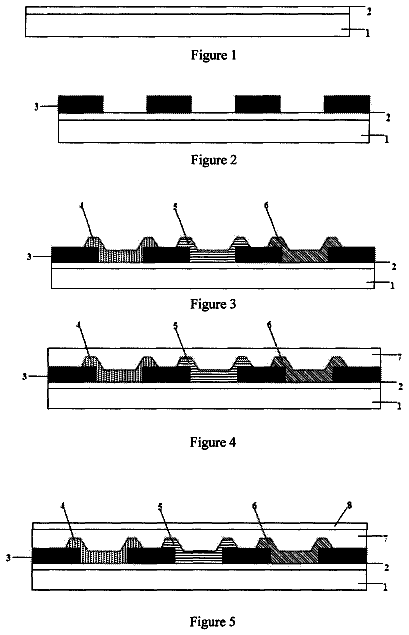
A color filter substrate includes a first linear pattern formed of a first color filter, a second linear pattern formed of the first color filter, and a third linear pattern formed of a third color filter dividing the first pattern from the second linear pattern. In the present embodiment, the adjacently located first, second and third color filters with no gap therebetween have no formation of projections in a film thickness direction, the projections being ascribed to at least two color filters of different colors overlapped with each other in a thickness direction of the color filter substrate. In other words, the first, second and third color filters are formed such that no projections are formed in the film thickness direction, the projections being ascribed to at least two color filters of different colors overlapped with each other. Further, in other words, in the first, second and third color filters, two color filters are in contact with each other only via their side faces.
The color filters adjacent to each other in this way are formed in a heat treatment process (reflow processing) of a manufacturing process, by having one color filter material melted and contacted with a side face of another color filter that have been firstly formed on the substrate. The heat treatment processing is performed so that the melted color filter material does not flow toward the upper surface of the firstly fixed and formed color filter.
Further, in order to realize a structure in which the mutually adjacent color filters do not overlap in the thickness direction, it is preferable that the color filter firstly formed on the substrate has a cross sectional in a rectangular shape. The color filter having a rectangular cross section has a side face that is vertical to the substrate, and thus the subsequently formed color filter is arranged so as to be in contact with the vertical side face. Thus, the mutually adjacent color filters are arranged sandwiching their vertical side faces, thereby realizing the structure of the present invention in which no projection is formed.
It should be noted that the projection herein has a height that is equal to or more than a wavelength of light (e.g., 550 nm) that is liable to influence liquid crystal display. In the present embodiment, in arranging the first, second and third color filters with no gap therebetween, a very small degree of alignment error and bleeding may be tolerated. For example, quite a small degree of alignment error equal to or more than ½ of the wavelength of light which is liable to influence liquid crystal display, may be construed as corresponding to “no projection is formed” of the present embodiment. For example, in the event that a very small uplift is caused in a color filter due such as to bleeding of a color, this may be construed as corresponding to “no projection is formed” of the present embodiment. Further, in the heat treatment processing, in the event that the melted color filter is formed slightly covering a corner portion formed between the upper surface and the side face of the firstly formed color filter, this may be construed as corresponding to “no projection is formed” of the present embodiment.
The present embodiment is described by way of an example in which a color filter substrate is provided to a liquid crystal display device, but the color filter substrate may be provided to an organic EL display device.
FIGS. 1A to 1C are plan views illustrating an example of a color filter substrate 1 according to the present embodiment.
The color filter substrate 1 includes, in plan view, an effective display region 2 and a frame region 3 . The frame region 3 encloses the effective display region 2 . The effective display region 2 includes a plurality of areas 4 . In FIGS. 1A to 1C , the effective display region 2 includes a total of sixteen areas 4 , i.e. four in a longitudinal direction and four in a lateral direction. The number of the areas 4 included in the effective display region 2 can be changed according to the screen size of the liquid crystal display.
The color filter substrate 1 includes, in a plan view, two or more alignment marks 5 in the frame region 3 . The alignment marks 5 are used in the process of manufacturing the color filter substrate 1 . For example, the alignment marks 5 may be formed together with a firstly formed filter, with a color material of the firstly formed filter.
As a color filter CF, the color filter substrate 1 includes red filters RF, green filters GF and blue filters BF.
The red filters RF are each in a linear pattern which is long in a longitudinal direction.
The blue filters GF are also each in a linear pattern which is long in a longitudinal direction.
The green filters BF are each in a linear pattern which is long in a longitudinal direction and are each located between a red filter RF and a blue filter BF to isolate the red filter RF from the blue filter BF.
In the present embodiment, the lateral width of each red filter RF and the lateral width of each blue filter BF are W 1 . The lateral width of each green filter GF is W 2 . The width W 2 is substantially ½ of the lateral width W 1 .
The numerical value of substantially ½ as a ratio of the lateral width W 2 to the lateral width W 1 is specified so as to obtain a desired color balance and chromaticity of the red filters RF, the green filters GF and the blue filters BF. In order to obtain a desired color balance and chromaticity, the ratio of the lateral width W 2 relative to the lateral width W 1 may be slightly different from the numerical value ½.
Such red filters RF, the blue filters BF and the green filters GF are arranged in a stripe.
FIG. 2 is a cross-sectional view illustrating an example of the color filter substrate 1 . FIG. 2 corresponds to a cross section taken along A-A′ of FIG. 1C .
Further, FIG. 3 is a cross-sectional view illustrating an example of a liquid crystal panel 6 including the color filter substrate 1 . FIG. 3 corresponds to a cross section taken along B-B′ of FIG. 1A .
The color filter 1 includes a transparent substrate 7 , a color filter layer 8 , a transparent resin layer 9 and counter electrodes 10 . The counter electrodes 10 may be omitted.
As the transparent substrate 7 , glass is used, for example. The transparent substrate 7 has a first plane on which the color filter layer 8 is formed.
In the present embodiment, the color filter layer 8 includes the color filter CF, but may additionally include a light-shielding layer. The color filter CF includes the red filters RF, the blue filters BF and the green filters GF.
In the present embodiment, the color filter CF is formed over the effective display region 2 and the frame region 3 . In the color filter layer 8 , the thickness of the color filter CF in the effective display region 2 is substantially the same as the thickness of the color filter CF in the frame region 3 .
The transparent resin layer 9 is formed on the color filter layer 8 .
The counter electrodes 10 are formed on the transparent resin.
The counter electrodes 10 each have a linear pattern which is long in a longitudinal direction, and are formed along the respective red filters RF, the blue filters BF and the green filters GF.
The counter electrodes 10 may be formed, for example, into comb-shaped, band-shaped, linear or striped patterns.
The counter electrodes 10 may contain an electrically conductive metal oxide. As the electrically conductive metal oxide, for example, a transparent electrically conductive film such as Indium-Tin-Oxide (ITO) can be used.
In the present embodiment, the counter electrodes 10 overlap with the respective red, blue and green filters RF, BF and GR in a thickness direction.
In the present embodiment, the red, blue and green filters RF, BF and GR adjacent to each other with no gap therebetween do not substantially overlap with each other in a thickness direction even when an adjacent portion includes an irregularity of not more than ½ of the wavelength of light.
The liquid crystal panel 6 includes an array substrate 11 , a color filter substrate 1 and a liquid crystal layer 12 . The liquid crystal panel 6 has a front side (observer side or a surface of the color filter substrate 1 ) which is provided with a polarizing plate 131 . The liquid crystal panel 6 has a back side (inner side of the liquid crystal display device or a surface of the array substrate 11 ) which is provided with a polarizing plate 132 . The liquid crystal display device includes a light control element and a backlight unit under the liquid crystal panel 6 shown in FIG. 3 . The liquid crystal display device provided with the liquid crystal panel 6 is in black state of display when no liquid crystal drive voltage is applied. Unlike the liquid crystal orientation method with initial horizontal orientation called IPS (horizontal electric field method using horizontally oriented liquid crystal molecules) or ECB (Electrically Controlled Birefringence), no deviation is caused between the orientation direction of the liquid crystal molecules and the optical axes of the polarizing plates 131 and 132 , and thus a pitch black display (deep black display) can be obtained.
The array substrate 11 and the color filter substrate 1 face with each other. The liquid crystal layer 12 is sandwiched between the array substrate 11 and the color filter substrate 1 .
The liquid crystal layer 12 is arranged so as to face the counter electrodes 10 of the color filter substrate 1 . The transparent substrate 7 of the color filter substrate 1 has a second plane that is a display surface of the liquid crystal panel 6 , or a surface that an observer observes.
The array substrate 11 includes a transparent substrate 14 , insulating layers 15 a to 15 c , a common electrode, a pixel electrode and a liquid crystal drive element (active element). The common electrode and the pixel electrode however are omitted from FIG. 3 . For example, the liquid crystal drive elements that can be used may be thin-film transistors.
For example, a glass plate can be used as the transparent substrate 14 .
The transparent substrate 14 has a first plane on which the insulating layers 15 a and 15 b are formed. The common electrode is formed on the insulating layer 15 b . The insulating layer 15 c is formed on the insulating layer 15 b on which the common electrode is formed. The pixel electrode is formed on the insulating layer 15 c . As the insulating layers 15 a to 15 c , a mixture that contains, for example, SiN, SiO.sub.2, or SiN and SiO.sub.2 may be used. The pixel electrode and the common electrode, not shown, may contain electrically conductive metal oxide. For example, a transparent electrically conductive film that contains ITO or the like as the electrically conductive metal oxide can be used.
The liquid crystal layer 12 is arranged so as to face the pixel electrode of the array substrate 11 . The transparent substrate 14 of the array substrate 11 has a second plane which is located inside the liquid crystal display device.
The polarizing plate 131 is provided to the second plane (display surface of the liquid crystal panel 6 ) of the transparent substrate 7 . The polarizing plate 132 is provided to the second plane (inside the device of the liquid crystal panel 6 ).
In the present embodiment, the alignment marks 5 may be formed of a first color of the color filter CF. The alignment marks 5 are formed at least at two positions on the transparent substrate 7 . The alignment marks 5 are used for alignment in an exposure processing that follows the formation of a coating film of a photoresist that is a material of the color filter CF.
Hereinafter is described a method for manufacturing the color filter substrate 1 according to the present embodiment.
FIGS. 4A to 4G are state-transition diagrams illustrating an example of a method for manufacturing the color filter substrate 1 .
Apparatus used for manufacturing the color filter substrate 1 includes, for example, a resist coater, a dryer, an exposure apparatus, a developing apparatus and a film curing apparatus. Typical dryers and film curing devices that can be used include a clean oven, a hot plate, and the like.
The description continues in the full USPTO document.
 Lapsed, fee not paid5 drawings