Lapsed, fee not paid6 drawings
Chips & Semiconductors · US 9,748,467 B2
Piezoelectric vibrator
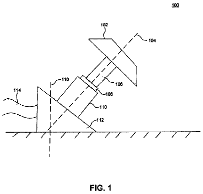
A piezoelectric vibrator element is more stably bonded to reduce the displacement with respect to an external force.
US 9,751,755 B2 · Assignee: Hewlett-Packard Development Company, L.P. · Inventors: Mardilovich; Peter et al.
Sheet 1 of 16 from the published document. All sheets in the USPTO PDF
A method of forming a micro-structure involves forming a multi-layered structure including i) an oxidizable material layer on a substrate and ii) another oxidizable material layer on the oxidizable material layer. The oxidizable material layer is formed of an oxidizable material having an expansion coefficient, during oxidation, that is more than 1. The method further involves forming a template, including a plurality of pores, from the other oxidizable material layer, and growing a nano-pillar inside each pore. The nano-pillar has a predefined length that terminates at an end. A portion of the template is selectively removed to form a substantially even plane that is oriented in a position opposed to the substrate. A material is deposited on at least a portion of the plane to form a film layer thereon, and the remaining portion of the template is selectively removed to expose the nano-pillars.
The present disclosure relates generally to methods of forming a micro-structure. Porous anodic oxide structures may be used in a variety of applications including, but not limited to, micro- and nano-electronics (such as, e.g., in planarized aluminum interconnections, precision thin-film resistors, thin-film capacitors, and nano-structured field-emission cathodes), electrostatic and thermo-activated switching devices, LC high-frequency oscillators, AC amplifiers, triggers and other logic vacuum integrated circuits (VICs), gas micro- and nano-sensors, micro- and nano-channel plates, mesoscopic engines, wavelength-sensitive filters, reflective and absorbing surfaces, membranes, nozzles, precision apertures, and/or like. These anodic oxide structures may also include one or more arrays of nano-pores that are used, for example, to form structures having one or more arrays of nano-pillars fo
8 of 16 drawing sheets so far from the published document, cropped to the drawing. Every sheet is in the USPTO PDF.
What the patent claimed, word for word. All of it is now free to use.
The present disclosure relates generally to methods of forming a micro-structure.
Porous anodic oxide structures may be used in a variety of applications including, but not limited to, micro- and nano-electronics (such as, e.g., in planarized aluminum interconnections, precision thin-film resistors, thin-film capacitors, and nano-structured field-emission cathodes), electrostatic and thermo-activated switching devices, LC high-frequency oscillators, AC amplifiers, triggers and other logic vacuum integrated circuits (VICs), gas micro- and nano-sensors, micro- and nano-channel plates, mesoscopic engines, wavelength-sensitive filters, reflective and absorbing surfaces, membranes, nozzles, precision apertures, and/or like. These anodic oxide structures may also include one or more arrays of nano-pores that are used, for example, to form structures having one or more arrays of nano-pillars formed on and supported by a substrate. In some cases, the structures may be insensitive to vibration (i.e., brittle). This may be due, at least in part, to a lack of internal structural flexibility of the structures themselves.
Features and advantages of embodiments of the present disclosure will become apparent by reference to the following detailed description and drawings, in which like reference numerals correspond to similar, though perhaps not identical, components. For the sake of brevity, reference numerals or features having a previously described function may or may not be described in connection with other drawings in which they appear.
FIGS. 1A through 1I together schematically depict an embodiment of a method of forming an embodiment of a micro-structure;
FIGS. 1A through 1G, 1J, and 1K together schematically depict another embodiment of the method of forming another embodiment of a micro-structure;
FIG. 2A is a schematic three-dimensional representation of the porous anodic alumina template prior to complete anodization of the aluminum;
FIG. 2B is a top view of the example of the anodic alumina template of FIG. 2A ;
FIG. 2C is a scanning electron micrograph (SEM) image showing a cross section of an anodic alumina template after about 30 minutes of etching;
FIG. 3 is a schematic side view of an example of a master that can be used to form an embodiment of an anodic alumina template;
FIGS. 4A through 4D are scanning electron micrograph (SEM) images of a top view ( FIG. 4A ), a cross-section ( FIG. 4B ), another top view at a higher magnification than that shown in FIG. 4A ( FIG. 4C ), and a tilted view ( FIG. 4D ) of a micro-structure including nano-pillars having a diameter of about 65 nm and a gap between adjacent nano-pillars of about 105 nm;
FIGS. 5A through 5D are SEM images of a top view ( FIG. 5A ), a cross-section ( FIG. 5B ), another top view at a higher magnification than that shown in FIG. 5A ( FIG. 5C ), and a tilted view ( FIG. 5D ) of a micro-structure including nano-pillars having a diameter of about 30 nm and a gap between adjacent nano-pillars of about 50 nm;
FIGS. 6A through 6D are SEM images of a top view ( FIG. 6A ), a cross-section ( FIG. 6B ), another top view at a higher magnification than that shown in FIG. 6A ( FIG. 6C ), and a tilted view ( FIG. 6D ) of a micro-structure including nano-pillars having a diameter of about 15 nm and a gap between adjacent nano-pillars of about 25 nm;
FIG. 7 is a top view schematically depicting an example of a micro-structure formed according to the embodiment of the method described in conjunction with FIGS. 1A through 1G, 1J, and 1K ;
FIG. 8 schematically depicts another example of a micro-structure that may be used for micro- or nano-filtration;
FIG. 9 is a SEM image of an example of a micro-structure being used as a filter for latex ink particles; and
FIG. 10 is a schematic diagram of another embodiment of the micro-structure of FIG. 1K used as a filter for gas filtration and sensing.
Embodiment(s) of the method disclosed herein may be used to form a micro-structure having an internal structure that is flexible enough so that the micro-structure may suitably be used as a shock absorber, a sensor, and/or the like. Devices made with or incorporating the micro-structure disclosed herein are considered to be robust, at least in part because of the built in shock absorbing property of the nano-structure. This is due, at least in part, to the fact that the weakest part of the structure, i.e., the nano-pillars, are built from amorphous oxide (i.e., no microcrystals with grain boundaries) and are built from the same material as the underlying support (i.e., no interfaces are present between the nano-pillars and the underlying dense oxide). As such, when exposed to external forces (e.g., mechanical pressure) the nano-pillars bend rather than break.
The micro-structure disclosed herein may include components that are on the micro-scale (i.e., from 1 μm to 1000 μm) and components that are on the nano-scale (i.e., from 1 nm to 1000 nm). In some cases, the micro-structure may also be used as a micro- or nano-fluidic device. As used herein, a “microfluidic device” refers to a device for capturing or separating micrometer-sized or smaller particulates within a fluid sample, whereas a “nanofluidic device” refers to a device for capturing or separating nanometer-sized or smaller particulates within a fluid sample. Examples of micro- or nano-fluidic devices include lab-on-a-chip devices, devices for the detection of an analyte, filtration devices, and/or devices for separation of fluidic media.
Briefly, the micro-structure formed by embodiment(s) of the method disclosed herein includes a plurality of micro-islands supported by a set of nano-pillars. As used herein, a “micro-island” is a dense or non-porous film or layer established on a pre-designated set of nano-pillars. The combination of the micro-island and the set of nano-pillars upon which the micro-island is formed may be referred to herein as a “micro-cluster”. In some instances, the term micro-cluster may be used interchangeable with the term “multi-legged table structure”.
One example of the micro-structure is identified by reference numeral 100 shown in FIG. 1I , another example of the micro-structure is identified by 100 ′ shown in FIG. 1K , and still other examples of the micro-structure are identified by 100 ″ and 100 ′″ are shown, respectively, in FIGS. 8 and 10 . It is to be understood that the embodiment(s) of the method may be used to selectively control the placement of each nano-pillar in the micro-structures 100 , 100 ′, 100 ″, 100 ′″ so that each nano-pillar is substantially uniformly spaced from an adjacent nano-pillar and/or each set of nano-pillars (e.g., for a micro-cluster) is substantially uniformly spaced from an adjacent set of nano-pillars. In other words, the size of a gap formed between adjacent nano-pillars or sets of nano-structures may be selectively controlled. In instances where the nano-structure is used as a micro- or nano-filter, the controlled size of the gap at least between adjacent nano-pillars advantageously improves the selectivity of the device. Furthermore, the nano-structures 100 , 100 ′, 100 ″, 100 ′″ enable micro- or nano-filtration of fluidic media in a vertical direction (see, e.g., FIG. 8 ) or in a lateral direction (see, e.g., FIG. 10 ). Vertical filtration enables the filtrate to reach a substrate surface relatively quickly. This may be desirable when the substrate surface is a sensing surface. Lateral filtration provides a path for effective separation. The embodiments of the structure 100 , 100 ′, 100 ″, 100 ′″ can improve both the selectivity and efficiency of the filtration process.
The embodiment(s) of the method may also be used to control other properties of the nano-pillars. The geometry and/or dimensions of the nano-pillars (such as their height, diameter, shape, etc.) may be controlled by adjusting one or more parameters of the anodizing process employed in the instant methods. The process(es) used for controlling the property/ies of the nano-pillars will be described in further detail below. In one example, the geometry of the nano-pillars may be controlled so that the nano-pillars each have a uniform aspect ratio (where the difference between nano-pillars does not exceed 10%). This imparts at least some flexibility to the micro-structures 100 , 100 ′, 100 ″, 100 ′″ so that the micro-structures 100 , 100 ′, 100 ″, 100 ′″ can be used as shock absorbers. The control allowed throughout the processes disclosed herein enables process uniformity and reproducibility at least up to the wafer level.
One embodiment of the method of forming the nano-structure 100 (depicted in FIG. 1I ) is schematically depicted in FIGS. 1A through 1I , while another embodiment of the method of forming the micro-structure 100 ′ (depicted in FIG. 1K ) is schematically depicted in FIGS. 1A through 1G, 1J, and 1K . As mentioned above, still another embodiment of forming the micro-structure 100 ′″ (depicted in FIG. 10 ) is described below in conjunction with FIG. 10 . The micro-structures 100 , 100 ′, 100 ″, 100 ′″ formed by the embodiments of the instant method may, in some instances, be planar structures that, as mentioned above, may be used as shock absorbers, sensors, and/or the like. In some cases, as also mentioned above, the micro-structures 100 , 100 ′, 100 ″, 100 ′″ may also be used as micro- or nano-filters for liquid filtration/separation. The micro-structures 100 , 100 ′, 100 ″, 100 ′″ may also be used for gas filtration/separation, such as, for example, when portions of the nano-structures 100 , 100 ′, 100 ″ are exposed to air, it may be desirable to filter out particles from the air that should not reach a sensor (see, e.g., FIG. 5 discussed further hereinbelow). It is to be understood, however, that the micro-structures 100 , 100 ′, 100 ″, 100 ′″ may also be used for other applications, such as for actuators, pumps, or for delivery of small and discrete quantities of liquid to a particular location, for example, via a capillary effect (where liquid is sucked into spaces between the pillars when the surface properties (e.g., surface tension, contact angle, etc.) of the pillars are aligned with the properties of the liquid).
Referring now to FIG. 1A , the method of forming the nano-structure 100 includes forming a multi-layered structure 10 that contains i) an oxidizable material layer 14 established on a substrate 12 , and ii) another oxidizable material layer 16 established on the oxidizable material layer 14 . The multi-layered structure 10 may be formed, for example, by depositing an oxidizable material on the substrate 12 to form the oxidizable material layer 14 having a thickness, and then depositing another oxidizable material on the oxidizable material layer 14 to form the other oxidizable material layer 16 , which also has a thickness. In one embodiment, the oxidizable material layer 14 is formed of a metal or metal alloys that forms a dense oxide after electrochemical oxidation and the other oxidizable material layer 16 is formed of a metal or metal alloy that forms a porous oxide after electrochemical oxidation. Examples of suitable materials will be discussed further hereinbelow.
The layers 14 , 16 have respective thicknesses that may be different or may be substantially the same. In one embodiment, the thickness of each of the layers 14 , 16 ranges from about 10 nm to about 10 μm. The layer 14 may have any suitable thickness that will produce (during electrochemical oxidation) enough oxide to form the nano-pillars 20 . In an example, the thickness of the oxide grown from the layer 14 (i.e., the structure 14 ′, the nano-pillars 20 , and the cap layer 22 ) is determined by multiplying the anodization voltage by an anodization coefficient (i.e., the number of nanometers that the oxide grows per one volt of anodization voltage). For instance, for a Ta layer 14 , about 1.8 nm of Ta.sub.2O.sub.5 grows per volt of anodization voltage applied to the layer 14 to form a dense Ta.sub.2O.sub.5 film. In another instance, from about 1.3 nm to about 1.8 nm of Ta.sub.2O.sub.5 grows per volt of anodization voltage applied to the layer 14 to form nano-pillars with an underlying dense Ta.sub.2O.sub.5 film. In the latter instance (i.e., when there is a dense Ta.sub.2O.sub.5 film beneath the nano-pillars), the anodization coefficient depends, at least, on the diameter of the pores in the template 16 ′, the overall porosity of the template 16 ′, the nature of the electrolyte used for Ta anodization, and the current density during Ta anodization.
The thickness of the Ta layer 14 should be thick enough to produce a Ta.sub.2O.sub.5 layer having any desired thickness and, in some cases, to maintain some of the Ta layer 14 on the substrate 12 underneath the formed nano-pillars 20 and the dense portion of Ta.sub.2O.sub.5 (i.e., 14 ′). For example, to produce a dense Ta.sub.2O.sub.5 layer with no nano-pillars, the total thickness of the Ta layer 14 may be calculated by i) multiplying the completed anodization voltage (i.e., the specific voltage at which the oxide thickness reaches a steady state value) by 1.8 nm of Ta.sub.2O.sub.5 growth per volt to determine the thickness of Ta.sub.2O.sub.5 that grows, and ii) then dividing that number by the expansion coefficient (i.e., the ratio of Ta.sub.2O.sub.5 to consumed Ta), which is 2.3. For instance, if an anodization voltage of 200 V is used and 1.8 nm of Ta.sub.2O.sub.5 grows per volt (which produces about 360 nm of Ta.sub.2O.sub.5), and the expansion coefficient is 2.3, then the thickness of the Ta layer 14 is about 160 nm. In instances where nano-pillars, with an underlying dense Ta.sub.2O.sub.5 film, are grown from the Ta layer 14 , the thickness of the Ta layer 14 is based, at least in part, on the volume of Ta.sub.2O.sub.5 (which depends, at least in part, on the fraction of pillars in the entire stack, as well as their filling factor, i.e., pillar density) and the anodization coefficient (which depends, at least in part, on the electrolyte used and the anodization conditions, and is from about 1.3 nm to about 1.8 nm per volt for tantalum). The following is an example of how the Ta layer thickness is calculated when it is desirable to form both nano-pillars and the underlying dense layer. In this example, the nano-pillars with an underlying dense Ta.sub.2O.sub.5 layer are fabricated at 200 V. The height of pillars is 240 nm and the dense layer is 50 nm. The anodization coefficient is 1.45 nm/V. The pillar filling factor (or pillars density) is around 25%. In this example, nano-pillars of 240 nm are equivalent to 60 nm of dense Ta.sub.2O.sub.5, and thus there is a total of 110 nm of dense Ta.sub.2O.sub.5 that will be formed. In order to generate 110 nm of dense Ta.sub.2O.sub.5, at least about 50 nm of Ta is used in layer 14 (i.e., 110/2.3≈47.8). In other examples, these calculations may be performed assuming that the overall density of the nano-pillars is about 90%.
The thickness of the layer 16 , on the other hand, should be thick enough to form a template 16 ′ (see FIG. 1B ) that has a height that greater than the height of the nano-pillars 20 to be grown from the layer 14 . In one example, the layer 16 has a thickness of 100 nm or less. In another example, the layer 16 has a thickness of 50 nm or less. In still another example, the thickness of the template 16 ′ is about the thickness of the layer 16 times the expansion coefficient (e.g., about 1.3, which is the ratio between the thickness of the porous anodic alumina and the thickness of the aluminum layer 16 consumed).
In an example, each of the layers 12 , 14 are planar (e.g., are substantially flat and may include, if any, a minimal amount of irregularities). In another example, one or more of the layers 14 , 16 are non-planar. In this example, the non-planar layer(s) 14 , 16 may also include a special morphology, features, structures, and/or the like that are etched into or incorporated into the layers 14 , 16 . The planar or non-planar layers 14 , 16 may be deposited on a planar or non-planar substrate 12 , which will be described further below.
The deposition of the oxidizable material on the substrate 12 and the deposition of the other oxidizable material on the oxidizable material layer 14 may be accomplished using any suitable deposition technique known in the art. Some examples of suitable deposition techniques include physical vapor deposition (PVD) (such as, e.g., sputtering, thermal evaporation, and/or pulsed laser deposition), atomic layer deposition (ALD), or, in some instances, chemical vapor deposition (CVD).
The substrate 12 upon which the oxidizable material is deposited to form the layer 14 may be chosen based, at least in part, on the application for which the micro-structure 100 will ultimately be used. If, for example, the micro-structure 100 is to be used for semiconductor applications, the substrate 12 may be chosen from suitable support structures for semiconductors such as, e.g., a substantially planar silicon wafer. By “substantially planar”, it is meant that the surface is flat but may contain some irregularities. In this example, the substrate 12 may have formed thereon a layer of insulating material (not shown) such as, e.g., silicon oxide or silicon nitride. The substrate 12 may also or otherwise be a non-planar structure, e.g., the substrate 12 may have a special morphology etched on or fabricated into the substrate 12 . The substrate 12 may also be chosen from other materials such as, e.g., glass, quartz, alumina, stainless steel, plastic, and/or the like, and/or combinations thereof. In instances where the micro-structure 100 is used as a filter, the substrate 12 may be chosen from a silicon wafer having a thermally grown oxide (TOX) layer thereon, such as TOX/Si or SiO.sub.2/Si. In an example, TOX/Si may be formed by oxidizing Si at a high temperature (i.e., from about 800° C. to about 1200° C.) using water vapor (steam) or molecular oxygen as the oxidant. In other words, TOX/Si may be formed via dry or wet oxidation, and the TOX/Si oxide layer may be referred to as a high temperature oxide layer. In some cases, a dry oxygen atmosphere produces a higher quality SiO.sub.2, but the process itself is relatively slow. For thicker TOX/Si layers (i.e., a thickness of about 0.5 μm to about 4 μm or more), oxidation of the Si in a wet oxygen atmosphere is desirable. Other examples of TOX include, but are not limited to, SiN, SiC, TEOS (which is SiO.sub.2, but is prepared using a chemical vapor deposition (CVD) method from tetra-ethyloxy-silane (i.e., tetra-ethyl-ortho-silicate)), or the like.
The oxidizable material for the oxidizable material layer 14 is a conductor and may be chosen from a material that i) can be electrochemically oxidized and ii) has an expansion coefficient, during oxidation, that is more than 1. In some cases, the oxidizable material for the layer 14 may also or otherwise be thermally oxidized. In one embodiment, the oxidizable material layer 14 includes a material having an expansion coefficient that is more than 1. Without being bound to any theory, it is believed that an expansion coefficient of more than 1 allows the oxidizable material to squeeze into the pores 18 of the template 16 ′ (which will be described in further detail below). It is further believed that the height of the nano-pillars 20 that are formed may, at least partially, be based on the expansion coefficient of the material in the layer 14 . In an example, a nano-pillar 20 height ranging from about 10 nm to 1000 nm may be achieved when the expansion coefficient of the oxidizable material in layer 14 is more than 1. It is to be understood that the height of the nano-pillars 20 (including the thickness of structure 14 ′) may also be based, at least in part, on other factors including the anodization voltages used during the respective anodization of layers 16 and 14 . Further details about the height of the nano-pillars 20 will be described below. Some examples of suitable oxidizable materials include tantalum (which has an expansion coefficient for thermal oxidation of 2.3, as mentioned above), titanium (which has an expansion coefficient for thermal oxidation of 1.7), niobium (which has an expansion coefficient for thermal oxidation of 2.7), and tungsten (which has an expansion coefficient for thermal oxidation of 3.3). It is to be understood that the expansion coefficient for thermal oxidation for each of the foregoing materials is substantially the same as that for electrochemical oxidation so long as the phase of each of these materials during oxidation is the same.
The other oxidizable material for the other oxidizable material layer 16 is also a conductor, but is chosen from a metal or metal alloy that, after electrochemical oxidation, produces a porous oxide. One example of the other oxidizable material includes aluminum or aluminum alloys, such as an aluminum alloy having aluminum as the main component. It is further to be understood that silicon, titanium, tantalum, niobium, and tungsten in the aluminum alloy may be present in small quantities such as, e.g., up to about 5%. Another example of the other oxidizable material includes titanium, where such material may be oxidized using an appropriate electrolyte and anodization conditions to ultimately produce a porous oxide. In still another embodiment, the material layer 16 may be formed of silicon. When silicon is selected, field assisted anisotropic etching of silicon may take place in the presence of an HF-based electrolyte to create a porous silicon template, which is then oxidized to form a porous silicon dioxide template. It is believed that the layer 14 can still be anodized in the desirable manner when porous silicon dioxide is used as the template 16 ′. In yet another example, it is believed that the silicon may be transformed into Si.sub.xN.sub.y, which is not an oxide but is a dielectric and may be used as a template for Ta.sub.2O.sub.5 nano-pillar growth.
The oxidizable material forming the oxidizable material layer 14 and the other oxidizable material forming the other oxidizable material layer 16 are substantially pure. As used herein, the term “substantially pure” refers to a material (such as a metal or a metal alloy) having a minimal amount, if any, impurities present therein. In an example, a substantially pure metal may be one that includes at least 95% of the metal. In some cases the substantially pure metal includes about 100% metal, and thus practically no impurities. In these cases, the metal may be referred to as a substantially pure metal, a pure metal, or just a metal. In an example, the substantially pure metal has at least about a 99.9% (e.g., often expressed as 3N), and in some cases at least about 99.99% purity (e.g., often expressed as 4N). It is to be understood that, in some instances, the oxidizable material and/or the other oxidizable material may be a metal alloy.
For purposes of illustration, the methods depicted in the FIG. 1 series will now be described using tantalum as the oxidizable material in the oxidizable material layer 14 , and aluminum as the oxidizable material in the other oxidizable material layer 16 . As such, in reference to FIGS. 1A through 1K , the layer 14 will be referred to as the tantalum layer 14 , and the layer 16 will be referred to as the aluminum layer 16 . However, as previously noted, the layers 14 and 16 are not to be construed as being limited to being formed of tantalum and aluminum, respectively, but can be any of the oxidizable materials listed herein for the respective layers 14 , 16 .
After the multi-layered structure 10 is formed, a template 16 ′ is formed out of the aluminum layer 16 , as shown in FIG. 1B . In one embodiment, the template 16 ′ is formed by anodizing the aluminum layer 16 . Anodization refers to the oxidation of less than the entire thickness of the layer being anodized. It is to be understood that enough of the aluminum layer 16 is anodized to form the desired template 16 ′, which includes a plurality of pores 18 defined therein and a barrier layer B of alumina that defines the bottom of each pore 18 . As illustrated in FIG. 1B , after template 16 ′ formation, there is some remaining non-anodized aluminum 16 (e.g., the pyramids of aluminum 16 ).
Referring back to FIG. 1B , anodization of the aluminum layer 16 to form the template 16 ′ may be accomplished by employing the aluminum layer 16 as the anode of an electrolytic cell and selecting at least one of H.sub.2SO.sub.4 (sulfuric acid), H.sub.3PO.sub.4 (phosphoric acid), C.sub.2H.sub.2O.sub.4 (oxalic acid), or H.sub.2CrO.sub.4 (chromic acid) as the electrolyte. These electrolytes form porous alumina rather than dense alumina. The electrolyte may be present in a water based solution. In one embodiment where the electrolyte is oxalic acid (C.sub.2H.sub.2O.sub.4), the electrolyte may be present, in solution with water, at a wt % ranging from about 1 wt % to about 5 wt %. In another embodiment where the electrolyte is H.sub.2SO.sub.4, the electrolyte may be present, in solution with water, at a vol % ranging from about 5 vol % to about 40 vol %. In some instances, certain additives (e.g., an alcohol, a surfactant, etc.) may also be added to the electrolyte solution. It is to be understood that the concentration of electrolyte in solution and the other conditions may vary as long as they are suitable for porous anodization (i.e., the formation of the porous template 16 ′). Any suitable cathode may be used, for example, aluminum or platinum (e.g., foil or mesh). A suitable amount of voltage and current is then applied to the electrolytic cell for an amount of time to anodize the aluminum layer 16 (i.e., where the anodized portion of the aluminum layer 16 is oxidized). The anodization of the aluminum layer 16 forms porous anodic aluminum oxide (i.e., porous anodic alumina), and allows the alumina to grow to a desired thickness.
The porous template 16 ′ is shown in FIG. 1B . It is to be understood that the pores 18 at this point in the process do not extend through to, and expose, the underlying tantalum layer 14 . The size of the pores 18 formed during anodization may be controlled through the selection of the electrolyte and the anodization conditions. For instance, for an alumina template, the diameter D of a cell 17 is about 2.8 nm per volt (e.g., when Al is used for layer 16 ), and the diameter d of the pore 18 depends on the electrolyte and the current density. In one embodiment, the diameter d of the pore 18 is proportional to the voltage used. The ratio of the cell diameter and the pore diameter (D/d) is, for example, 3.3 for a H.sub.2CrO.sub.4 electrolyte, 4.9 for a H.sub.2SO.sub.4 electrolyte, 3.0 for a H.sub.2C.sub.2O.sub.4 electrolyte, and between 1.7 and 2.1 for a H.sub.3PO.sub.4 electrolyte. As some examples, pores of the following sizes may be obtained using the following electrolytes: pores having about 20 nm diameters may be obtained using H.sub.2SO.sub.4 as the electrolyte, pores having about 40 nm diameters may be obtained using C.sub.2H.sub.2O.sub.4 as the electrolyte, and pores having about 120 nm may be obtained using H.sub.3PO.sub.4 as the electrolyte. The size of the pores 18 may also be controlled via anisotropic etching after anodization is complete. This etching process further defines the already formed pores 18 , and in many instances increases the diameter of the formed pores 18 . Anisotropic etching may be performed using diluted phosphoric acid (5 vol. %), a solution of H.sub.2SO.sub.4 (20 vol. %), or a diluted form of a hydroxide such as, e.g., NaOH or KOH. The time for etching may vary, depending, at least in part, upon the desirable average diameter for the final pores 18 . In an embodiment, the anisotropic etching time ranges from about 1 minute to about 45 minutes in instances where anisotropic etching is performed using a diluted phosphoric acid (5 vol. %). The temperature for etching may also depend upon the process and etchant used. In one embodiment, the etchant temperature ranges from about 0° C. to about 100° C. depending, at least in part, on the type of etchant used. In an example, the etchant temperature ranges from about 20° C. to about 40° C., for example, when a diluted phosphoric acid etchant is used.
In another embodiment, prior to performing anodization, the method includes patterning the aluminum layer 16 . Patterning may be accomplished via any suitable technique, and is used to perform localized anodization of the aluminum layer 16 . Any standard photolithography method may be utilized. One example of patterning with standard photolithography includes depositing a hard mask material (e.g., Si.sub.xN.sub.y such as SiN or Si.sub.3N.sub.4) on the aluminum layer 16 , and then using a photoresist to pattern the Si.sub.xN.sub.y material to allow localized exposure of aluminum. In an example, the mask is patterned to expose portion(s) of the aluminum to the electrolyte. In some cases, the aluminum may also be patterned and etched to produce clusters of aluminum (i.e., formed when areas of aluminum are etched, but the Ta is still present). In other cases, aluminum and tantalum are patterned and etched to produce clusters of aluminum/tantalum. In this example, the interface formed between the mask and the aluminum layer 16 is robust, which advantageously prevents separation of the layers during anodization. In one embodiment, the areas that remain exposed once the mask and photoresist are in position are subject to local anodization. The aluminum layer exposed via the patterned mask or the patterned aluminum layer (not shown) is then locally anodized, for example, by employing the exposed or patterned aluminum layer as the anode of an electrolytic cell, and employing any suitable cathode, such as aluminum (having a 99.99% purity) and/or platinum (foil or mesh). The electrolyte may be selected from any electrolyte that will suitably allow the formation of porous alumina. Some examples of the electrolyte include solutions of H.sub.2SO.sub.4, H.sub.3PO.sub.4, H.sub.2C.sub.2O.sub.4, and H.sub.2CrO.sub.4. A suitable voltage and current is then applied to the electrolytic cell for an amount of time to completely or fully anodize the patterned aluminum layer (i.e., where the entire thickness of the patterned aluminum layer is oxidized).
In still another embodiment, the template 16 ′ may be patterned by transferring a pattern from a master (see, e.g., reference numeral 28 in FIG. 3 ) onto the aluminum layer 16 (which may be annealed prior to the transfer). In one example, a SiC master having a surface with hexagonally-ordered array of convexes may be pressed against the aluminum layer 16 to form an array of concaves on the surface of the aluminum layer 16 . The aluminum layer 16 may thereafter be anodized via the method described above using a constant voltage (i.e., a potentiostatic regime). The dimensions of the master 28 are chosen for a specific anodic alumina cell diameter D, and as such, that master 28 is used to obtain a single cell diameter D and a single pore diameter d (noting that small differences may be expected for pore diameter d when different electrolytes and/or anodization voltages are used). This method forms a highly hexagonally-ordered array of pores (having uniform diameters) in the anodic alumina.
The combination of patterning and anodization forms a porous anodic alumina template 16 ′ with specific dimensions (e.g., a hexagonally-ordered array of pores). The template 16 ′ formed via this embodiment of the method may also be anisotropically etched as previously described to further define the pores 18 .
In one example, the anodization of the aluminum layer 16 may be accomplished via a potentiostatic regime, whereby a constant anodization voltage is applied. Due at least in part to the pore diameter being proportional to voltage, anodization using a constant voltage produces pores having a substantially constant diameter from top to bottom. In another example, the anodization may be accomplished via a galvanostatic regime, whereby a constant current density is applied, and thus a constant rate of anodization is achieved. In this example, the voltage may vary during the anodization, which produces pores having a varying diameter from top to bottom.
The anodic alumina template 16 ′ is schematically shown in FIG. 1B (cross-sectional view). Another example of the anodic alumina template 16 ′ (where a portion of the aluminum layer 16 remains) is shown in FIGS. 2A (perspective view), 2 B (top view), and 2 C (an SEM image of a cross section of the template 16 ′) where the template 16 ′ includes a plurality of cells 17 (see FIGS. 2A and 2B ) each having a pore 18 defined therein. It is to be understood that the SEM image shown in FIG. 2C was anisotropically etched for 30 minutes to increase the diameter of the pores 18 . In an example, each of the pores 18 defined in the template 16 ′ is oriented substantially normal to the substrate 12 surface.
Referring now to FIG. 1C , either anodization is continued or another anodization current and voltage is applied to initiate a plurality of steps that lead to complete anodization of the remaining aluminum layer 16 and the formation of tantalum pentoxide nano-pillars 20 (see FIGS. 1D and 1E ). The anodization process that oxidizes remaining aluminum 16 and oxidizes the tantalum 14 may be accomplished, for example, using the same process described above for initial anodization of the aluminum layer 16 (to form the template 16 ′). In one embodiment, the anodization of remaining portions of the aluminum layer 16 and the layer 14 is accomplished by employing the tantalum layer 14 as the anode of an electrolytic cell and employing platinum, stainless steel, or any other appropriate material as the cathode, and applying a suitable anodization voltage and/or current density to initiate the various processes described herein.
It is to be understood that the remaining aluminum layer 16 (e.g., aluminum fragments located between alumina cells 17 of the template 16 ′) may become anodized via a variety of methods. When the remaining aluminum layer 16 is anodized, it become alumina and essentially becomes part of the barrier layer B. This alumina barrier layer B is a dielectric layer between the electrolyte and the metal (in this case, tantalum).
It is to be understood that the remaining aluminum layer 16 can be anodized using the same electrolyte used to form the template 16 ′, or can be anodized using another electrolyte that results in the formation of dense (as opposed to porous) alumina. When the electrolyte used to form the template 16 ′ is used to oxidize the remaining aluminum layer 16 , the anodization process used for the aluminum layer 16 may simply be continued until complete aluminum anodization is achieved and the tantalum interface is reached (as indicated, for e.g., by the change in current density). In the embodiment where the electrolyte used to complete aluminum anodization is the same electrolyte that forms the porous template 16 ′, it is believed that the barrier layer B making up the bottom of the pores 18 is etched away by field assisted dissolving. This dissolution opens up the pores 18 to enable growth of tantalum pentoxide nano-pillars 20 therein. In this embodiment, tantalum anodization may be performed using the same electrolyte (i.e., the electrolyte that forms the porous template) or another electrolyte.
When the same electrolyte is used for template 16 ′ formation and tantalum layer 14 anodization, the anodization process is continued in order to begin the oxidation of the tantalum layer 14 . As shown in FIGS. 1B and 1C , in this embodiment, complete aluminum anodization (i.e., formation of the template 16 ′, oxidation of the remaining aluminum 16 , and dissolution of the bottom of each pore 18 ) and tantalum anodization may take place in the same electrolyte (e.g., oxalic acid). This electrolyte will form the template 16 ′, anodize remaining aluminum 16 , will dissolve alumina from the bottom of the pores 18 , and will subsequently grow a dense oxide from the layer 14 . This advantageously enables the barrier layer B at the bottom of each pore 18 to dissolve and the Ta.sub.2O.sub.5 to be generated at the same time, thus keeping the overall thickness of the oxide such that it corresponds to the applied voltage.
In another embodiment, complete aluminum anodization is performed in the electrolyte that results in the porous alumina template 16 ′ with open pores 18 (e.g., oxalic acid), and then the electrolyte may be switched to form the dense tantalum pentoxide. In this embodiment, the electrolyte used during the subsequent anodization is selected from citric acid (C.sub.6H.sub.8O.sub.7), boric acid (H.sub.3BO.sub.3), ammonium pentaborate ((NH.sub.4).sub.2B.sub.10O.sub.16×8H.sub.2O), ammonium tartrate (H.sub.4NO.sub.2CCH(OH)CH(OH)CO.sub.2NH.sub.4), mixtures thereof, or another suitable electrolyte. This electrolyte will form the dense tantalum pentoxide layer 14 ′ that will ultimately grow to form the nano-pillars 20 .
In still another embodiment (not shown in figures), after the template 16 ′ is formed and some aluminum layer 16 remains, another electrolyte (i.e., an electrolyte that results in the formation of a dense, rather than porous, alumina) is used to oxidize the remaining aluminum layer 16 and to grow the Ta.sub.2O.sub.5. In this embodiment, the electrolyte solution will be switched, and anodization of the remaining aluminum layer 16 and of the tantalum layer 14 will take place in this other electrolyte (examples of which include citric acid (C.sub.6H.sub.8O.sub.7), boric acid (H.sub.3BO.sub.3), ammonium pentaborate ((NH.sub.4).sub.2B.sub.10O.sub.16×8H.sub.2O), ammonium tartrate (H.sub.4NO.sub.2CCH(OH)CH(OH)CO.sub.2NH.sub.4), and/or another suitable electrolyte). In this embodiment, the anodization of the remaining aluminum layer 16 will form a dense alumina that increases the thickness of the barrier layer B, but will not open up the pores 18 . Without being bound to any theory, it is believed that when the electrolyte selected to anodize the remaining aluminum layer 16 forms dense alumina (e.g., electrolyte is citric acid), the growth of the tantalum pentoxide nano-pillars will push the remaining barrier layer B up through the pores 18 , which may be the source of alumina traces in the resulting nano-pillars 20 .
Whichever process and electrolyte is selected for tantalum layer 14 anodization, it is to be understood that as the anodization of the oxidizable material layer 14 (in this example the tantalum layer 14 ) continues, the oxidized form of the tantalum (i.e., tantalum pentoxide structure 14 ′) grows through the individual pores 18 defined in the template 16 ′ to form a nano-pillar 20 of tantalum pentoxide in each pore 18 , as shown in FIGS. 1D and 1E . This structure 14 ′ is grown from the tantalum layer 14 , and some of the structure 14 ′ grows through the pores 18 of the template 16 ′. The growing of the structure 14 ′ may be accomplished, for example, by partially anodizing the tantalum layer 14 (i.e., part of the layer 14 is oxidized, and part of the layer 14 remains non-oxidized) as previously described. As anodization continues, both the interface between the oxidizable material layer 14 and the formed anodic oxide (i.e., oxide structure) 14 ′ and the interface between the anodic oxide 14 ′ and the electrolyte (not shown) are planarized (see FIG. 1E ).
The description continues in the full USPTO document.
About 6,581 words. The USPTO PDF has it with every drawing.
Fees are due 3.5, 7.5 and 11.5 years after grant. This patent expired on September 5, 2025, so the fee marked "not paid" was the one that went unpaid.
METHOD OF FORMING A MICRO-STRUCTURE
Filed Oct 2010 · published Jul 2013Method of forming a micro-structure
Filed Oct 2010 · granted Sep 2017Earlier publications, parents and continuations. None of them can still be enforced, or this patent would not be listed.
Prior art cited by the examiner or applicant. Useful when you check your own idea for novelty.
Everything on this page comes from the documents linked above.