 Lapsed, fee not paid4 drawings
Cameras, Displays & Optics · US 9,733,487 B2
Retaining device
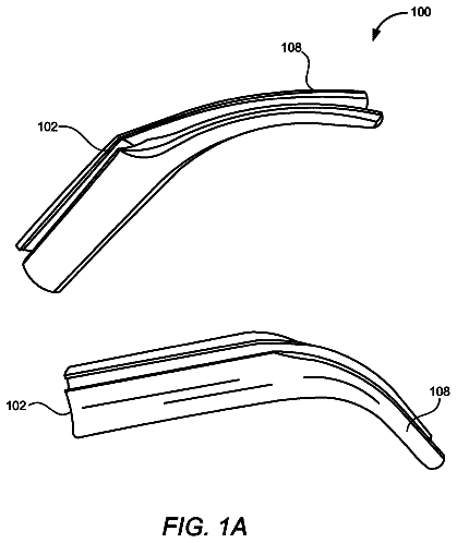
A retaining device joins with a frame from a pair of eyeglasses to securely retain the eyeglasses to the ears and head.
US 9,733,500 B2 · Assignee: Sony Corporation · Inventors: Ebisui; Akira et al.
Sheet 1 of 29 from the published document. All sheets in the USPTO PDF
An illumination unit includes a light modulation layer including a first region and a second region that have optical anisotropy and different responsiveness to an electric field. The light modulation layer satisfies an expression A/B<A 1 /B 1 when the light modulation layer exhibits the scattering characteristics.
The present application relates to an illumination unit that includes a light modulation device that exhibits scattering characteristics or transparency with respect to light, and also relates to a display. Recently, high image quality and energy saving in liquid crystal displays have been radically proceeded and there is proposed a scheme that achieves improvement in contrast in a dark place by partially modulating light intensity of a backlight. In this technique, mainly, a light emitting diode (LED) used as a light source of the backlight is partially driven to modulate light from the backlight in accordance to a display image. Also, a demand for reducing thickness has been increased in a large liquid crystal display as in a small liquid crystal display. Therefore, attention has been attracted not to a scheme that arranges, for example, a cold cathode fluorescent lamp (CCFL), an LED,
1 of 29 drawing sheets so far from the published document, cropped to the drawing. Every sheet is in the USPTO PDF.
What the patent claimed, word for word. All of it is now free to use.
The present application claims priority to Japanese Priority Patent Application JP 2012-116746 filed in the Japan Patent Office on May 22, 2012, the entire content of which is hereby incorporated by reference.
The present application relates to an illumination unit that includes a light modulation device that exhibits scattering characteristics or transparency with respect to light, and also relates to a display.
Recently, high image quality and energy saving in liquid crystal displays have been radically proceeded and there is proposed a scheme that achieves improvement in contrast in a dark place by partially modulating light intensity of a backlight. In this technique, mainly, a light emitting diode (LED) used as a light source of the backlight is partially driven to modulate light from the backlight in accordance to a display image. Also, a demand for reducing thickness has been increased in a large liquid crystal display as in a small liquid crystal display. Therefore, attention has been attracted not to a scheme that arranges, for example, a cold cathode fluorescent lamp (CCFL), an LED, or the like directly beneath the liquid crystal panel, but to an edge-light scheme that arranges a light source at an end of a light guide plate.
The present applicant has achieved partial drive that partially modulates light intensity of the light from the backlight in the edge-light scheme, and has disclosed the technique, for example, in Japanese Unexamined Patent Application Publication No. 2011-142065 (JP 2011-142065A). In JP 2011-142065A, a polymer dispersed liquid crystal (PDLC) is used in order to achieve the above-described partial drive. In JP 2011-142065A, the PDLC is formed by mixing a liquid crystal material and a low-molecular material with alignment properties and polimerizability and by causing phase-separation by ultraviolet irradiation, and the PDLC is a composite layer in which the liquid crystal material is dispersed in a polymer material having a streaky structure. The PDLC is classified into a horizontal alignment type, a vertical alignment type, and an isotropic type, depending on alignment upon no voltage application. Out of the foregoing types, the horizontal alignment type achieves high luminance and high contrast, and therefore, is most suitable for a backlight.
In the above-described PDLC of a horizontal alignment type, interfaces of the polymer material and the liquid crystal material are formed densely in a minor-axis direction of the streaky structure and is formed sparsely in a major-axis direction of the streaky structure. Therefore, when the streaky structure extends in a direction that is parallel to a light incident surface, light that propagates in the above-described minor-axis direction of the streaky structure inside the PDLC enters the interface with a cycle of average streaky organization size in the minor-axis direction of the streaky structure, and as a result, is scattered largely. On the other hand, light that propagates in the above-described major-axis direction of the streaky structure inside the PDLC has less opportunity to enter the interface, and therefore is not scattered much.
Moreover, light that propagates in a direction (hereinafter, referred to as “X direction”) that is the minor-axis direction of the streaky structure and is perpendicular to the light incident surface inside the PDLC propagates with a cycle of the average streaky organization size in the minor-axis direction of the streaky structure, with being influenced by a difference between an extraordinary refractive index of the liquid crystal material and an ordinary refractive index of the polymer material and by a difference between an ordinary refractive index of the liquid crystal material and an extraordinary refractive index of the polymer material. On the other hand, light that propagates in the above-described major-axis direction (hereinafter, referred to as “Y direction”) of the streaky structure inside the PDLC or in a thickness direction (hereinafter, referred to as “Z direction”) of the PDLC propagates being influenced only by the difference between the extraordinary refractive index of the liquid crystal material and the ordinary refractive index of the polymer material or by the difference between the ordinary refractive index of the liquid crystal material and the extraordinary refractive index of the polymer material. Therefore, light that propagates in the X direction inside the PDLC is scattered largely, and light that propagates in the Y direction and in the Z direction inside the PDLC is not scattered much.
As described above, in the PDLC of a horizontal alignment type, anisotropy of scattering is caused between light that propagates in the X direction and light that propagates in the Y or Z direction due to the above-described two factors. As a result, light that propagates in the Z direction is scattered preferentially in a direction in which a light guide condition is destroyed, and therefore, light extraction efficiency is increased. Accordingly, high luminance and high contrast are obtained.
However, when the PDLC of a horizontal alignment type is applied to a backlight of an edge-light scheme, luminance distribution is likely to be non-uniform between light that propagates in the X direction and light that propagates in the Y direction due to anisotropy in scattering. In particular, when arrangement pitches of respective point light sources in a linear light source is sparse, there has been an issue that bright-dark stripes may be caused in the vicinity of the linear light source.
It is desirable to provide an illumination unit capable of improving uniformity in luminance and a display that includes the illumination unit.
According to an embodiment of the present disclosure, there is provided an illumination unit including: a first transparent substrate and a second transparent substrate that are arranged to be separated from each other and to face each other; a light source applying light to an end face of the first transparent substrate; and a light modulation layer provided in a gap between the first transparent substrate and the second transparent substrate and exhibiting scattering characteristics or transparency with respect to the light from the light source depending on magnitude of an electric field, the light modulation layer including a first region that has optical anisotropy and relatively-high responsiveness to the electric field and a second region that has optical anisotropy and relatively-low responsiveness to the electric field, and the light modulation layer satisfying a following expression when the light modulation layer exhibits the scattering characteristics, A/B<A 1 /B 1
where A is magnitude of first scattering with respect to the light propagating in a first direction that is perpendicular to the end face; B is magnitude of second scattering with respect to the light propagating in a second direction that is parallel to the end face and is parallel to a surface of the first transparent substrate; A 1 is magnitude of scattering with respect to the light propagating in a direction perpendicular to the end face when an optical axis of the first region is in a direction of a normal to the first transparent substrate, and an optical axis of the second region is in a direction that is parallel to the end face and is orthogonal to the optical axis of the first region; and B 1 is magnitude of scattering with respect to the light propagating in a direction that is parallel to the end face and is parallel to the surface of the first transparent substrate when the optical axis of the first region is in the direction of the normal to the first transparent substrate and the optical axis of the second region is in a direction that is parallel to the end face and is orthogonal to the optical axis of the first region.
According to an embodiment of the present disclosure, there is provided a display provided with a display panel displaying an image by modulating light and an illumination unit illuminating the display panel from back thereof, the illumination unit including: a first transparent substrate and a second transparent substrate arranged to be separated from each other and to face each other; a light source applying light to an end face of the first transparent substrate; and a light modulation layer provided in a gap between the first transparent substrate and the second transparent substrate and exhibiting scattering characteristics or transparency with respect to the light from the light source depending on magnitude of an electric field, the light modulation layer including a first region that has optical anisotropy and relatively-high responsiveness to the electric field and a second region that has optical anisotropy and relatively-low responsiveness to the electric field, and the light modulation layer satisfying a following expression when the light modulation layer exhibits the scattering characteristics, A/B<A 1 /B 1
where A is magnitude of first scattering with respect to the light propagating in a first direction that is perpendicular to the end face; B is magnitude of second scattering with respect to the light propagating in a second direction that is parallel to the end face and is parallel to a surface of the first transparent substrate; A 1 is magnitude of scattering with respect to the light propagating in a direction perpendicular to the end face when an optical axis of the first region is in a direction of a normal to the first transparent substrate, and an optical axis of the second region is in a direction that is parallel to the end face and is orthogonal to the optical axis of the first region; and B 1 is magnitude of scattering with respect to the light propagating in a direction that is parallel to the end face and is parallel to the surface of the first transparent substrate when the optical axis of the first region is in the direction of the normal to the first transparent substrate and the optical axis of the second region is in a direction that is parallel to the end face and is orthogonal to the optical axis of the first region.
In the illumination unit and the display according to the embodiments of the present application, the light modulation layer has the configuration by which the foregoing expression is satisfied when the light modulation layer exhibits the scattering characteristics. Therefore, anisotropic scattering of the light that propagates in the first direction and the light that propagates in the second direction is moderated in whole of the light modulation layer.
According to the illumination unit and the display according to the embodiments of the present application, the light modulation layer has the configuration that satisfies the foregoing expression when the light modulation layer exhibits scattering characteristics. Therefore, the above-described anisotropic scattering is moderated in the whole of the light modulation layer. Here, the bright-dark stripes due to the arrangement of the light source are caused by a large difference between the first scattering and the second scattering. Therefore, contrast of the bright-dark stripes due to the arrangement of the light source is reduced by moderating the above-described anisotropic scattering in the whole of the light modulation layer. As a result, uniformity in luminance is improved.
It is to be understood that both the foregoing general description and the following detailed description are exemplary, and are intended to provide further explanation of the technology as claimed.
Additional features and advantages are described herein, and will be apparent from the following Detailed Description and the figures.
The accompanying drawings are included to provide a further understanding of the disclosure, and are incorporated in and constitute a part of this specification. The drawings illustrate embodiments and, together with the specification, serve to explain the principles of the technology.
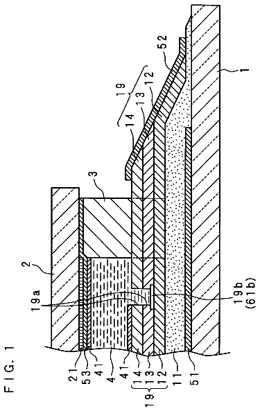
FIG. 1 is a diagram illustrating an example of a cross-sectional configuration of an illumination unit according to an embodiment of the present application.
FIG. 2 is a diagram illustrating an example of a cross-sectional configuration in an XZ plane of a light modulation device in FIG. 1 .
FIG. 3 is a plan view illustrating alignment directions of alignment films in FIG. 2 .
FIG. 4 is a diagram illustrating an example of a cross-sectional configuration in an XY plane of a light modulation layer in FIG. 2 .
FIG. 5 is a diagram illustrating another example of the cross-sectional configuration in the XY plane of the light modulation layer in FIG. 2 .
FIGS. 6A and 6B are diagrams illustrating an example of structural cycles in the light modulation layer in FIG. 2 .
FIG. 7 is a diagram illustrating an example of a proportion of a polymer region in the light modulation layer in FIG. 2 .
FIG. 8 is a diagram schematically illustrating an example of functions of the light modulation device in FIG. 1 .
FIG. 9 is a diagram schematically illustrating another example of the function of the light modulation device in FIG. 1 .
FIG. 10 is a diagram schematically illustrating an example of a function of the illumination unit in FIG. 1 .
FIG. 11 is a plan view illustrating alignment directions of alignment films according to a comparative example.
FIG. 12 is a diagram illustrating an example of a cross-sectional configuration in an XY plane of a light modulation layer according to the comparative example.
FIGS. 13A and 13B are diagrams illustrating an example of structural cycles in the light modulation layer in FIG. 12 .
FIG. 14 is a diagram schematically illustrating an example of functions of a light modulation device according to the comparative example.
FIG. 15 is a diagram schematically illustrating another example of the function of the light modulation device according to the comparative example.
FIGS. 16A to 16C are diagrams illustrating an example of a method of manufacturing the light modulation device in FIG. 1 .
FIGS. 17A to 17C are diagrams illustrating manufacturing processes following that in FIG. 16C .
FIGS. 18A to 18C are diagrams illustrating manufacturing processes following that in FIG. 17C .
FIG. 19 is a diagram illustrating an example of an outline configuration of an illumination unit according to a second embodiment of the present application.
FIG. 20 is a diagram illustrating an example of a cross-sectional configuration in an XZ plane of a light modulation device in FIG. 19 .
FIG. 21 is a plan view illustrating alignment directions of alignment films in FIG. 20 .
FIG. 22 is a diagram illustrating an example of a cross-sectional configuration in the XY plane of a light modulation layer in FIG. 20 .
FIGS. 23A and 23B are diagrams illustrating an example of structural cycles in the light modulation layer in FIG. 20 .
FIG. 24 is a diagram illustrating an example of a proportion of a polymer region in the light modulation layer in FIG. 20 .
FIG. 25 is a diagram schematically illustrating an example of functions of the light modulation device in FIG. 19 .
FIG. 26 is a diagram schematically illustrating another example of the functions of the light modulation device in FIG. 19 .
FIG. 27 is a diagram illustrating an example of an outline configuration of an illumination unit according to a third embodiment of the present application.
FIG. 28 is a diagram illustrating an example of a cross-sectional configuration in the XZ plane of a light modulation device in FIG. 27 .
FIG. 29 is a plan view illustrating alignment directions of alignment films in FIG. 28 .
FIG. 30 is a diagram illustrating an example of a cross-sectional configuration in the XY plane of a light modulation layer in FIG. 28 .
FIG. 31 is a diagram illustrating another example of the cross-sectional configuration in the XY plane of the light modulation layer in FIG. 28 .
FIGS. 32A and 32B are diagrams illustrating an example of structural cycles in the light modulation layer in FIG. 28 .
FIG. 33 is a diagram illustrating an example of proportion of a polymer region in the light modulation layer in FIG. 28 .
FIG. 34 is a diagram schematically illustrating an example of a function of the light modulation device in FIG. 27 .
FIG. 35 is a diagram schematically illustrating another example of the function of the light modulation device in FIG. 27 .
FIG. 36 is a diagram illustrating a first modification of the outline configurations of the illumination units in FIGS. 1, 19, and 27 .
FIG. 37 is a diagram illustrating a second modification of the outline configurations of the illumination units in FIGS. 1, 19, and 27 .
FIG. 38 is a diagram illustrating a third modification of the outline configurations of the illumination units in FIGS. 1, 19, and 27 .
FIG. 39 is a diagram illustrating a fourth modification of the outline configurations of the illumination units in FIGS. 1, 19, and 27 .
FIG. 40 is a diagram illustrating a fifth modification of the outline configurations of the illumination units in FIGS. 1, 19, and 27 .
FIG. 41 is a diagram illustrating a first modification of a light guide plate or a transparent substrate in the illumination units in FIGS. 1, 19, and 27 .
FIG. 42 is a diagram illustrating a second modification of the light guide plate or the transparent substrate in the illumination units in FIGS. 1, 19, and 27 .
FIG. 43 is a diagram illustrating a third modification of the light guide plate or the transparent substrate in the illumination units in FIGS. 1, 19, and 27 .
FIG. 44 is a diagram illustrating an example of a display according to a fourth embodiment of the present application.
Preferred embodiments of the present disclosure will be described below in detail with reference to the drawings. The description will be given in the following order. 1. First Embodiment (illumination unit)
An example using a horizontal alignment film (aligned at 0°) and a vertical alignment film 2. Second Embodiment (illumination unit)
An example using two horizontal alignment films (aligned at θ 1 °) 3. Third Embodiment (illumination unit)
An example using a horizontal alignment film (aligned at θ 1 °) and a horizontal alignment film (aligned at 0°). 4. Modifications (illumination unit) 5. Fourth Embodiment (display)
[1. First Embodiment]
[Configuration]
FIG. 1 illustrates an example of a cross-sectional configuration of an illumination unit 1 according to a first embodiment of the present application. FIG. 2 is a cross-sectional view illustrating an example of an outline configuration of a light modulation device 30 in the illumination unit 1 in FIG. 1 . It is to be noted that FIGS. 1 and 2 are mere schematic diagrams and dimensions and shapes illustrated therein are not necessarily the same as the actual ones. The illumination unit 1 emits illumination light from a top face thereof. The illumination unit 1 may be used, for example, for application of illuminating a component such as a liquid crystal display panel from the back thereof. The illumination unit 1 may include, for example, a light guide plate 10 , a light source 20 arranged on a side face of the light guide plate 10 , the light modulation device 30 and a reflective plate 40 arranged on the back of the light guide plate 10 , and a drive circuit 50 that drives the light modulation device 30 .
The light guide plate 10 guides light from the light source 20 arranged on the side face of the light guide plate 10 to the top face of the illumination unit 1 . The light guide plate 10 has a shape corresponding to a display panel (not illustrated) that is arranged on a top face of the light guide plate 10 , for example, a rectangular parallelepiped shape that is surrounded by a top face, a bottom face, and side faces. It is to be noted that, hereinafter, a side face which light from the light source 20 enters, out of the side faces of the light guide plate 10 , is referred to as a light incident surface 10 A. The light guide plate 10 may have a predetermined patterned shape on one or both of the top face and the bottom face thereof, and may have a function that scatters light entering from the light incident surface 10 A to be uniform, for example. The light guide plate 10 may function, for example, as a supporting member that supports an optical sheet (such as a diffusion plate, a diffusion sheet, a lens film, and a polarization separation sheet) arranged between the display panel and the illumination unit 1 . The light guide plate 10 may mainly include, for example, a transparent thermoplastic resin such as a polycarbonate resin (PC) and an acrylic resin (polymethyl methacrylate (PMMA)).
The light source 20 applies light to the side face of the light guide plate 10 . The light source 20 is a linear light source and, in particular, is configured of a plurality of LEDs arranged in a line. The LEDs are preferably white LEDs. It is to be noted that the plurality of LEDs may include, for example, a red LED, a green LED, and a blue LED. The light source 20 may be provided, for example, only on one side face of the light guide plate 10 as shown in FIG. 1 . It is to be noted that the light source 20 may be provided, for example, on both side faces of the light guide plate 10 , which is not illustrated.
The reflective plate 40 returns, toward the light guide plate 10 , light leaked out from the back of the light guide plate 10 through the light modulation device 30 . The reflective plate 40 may have, for example, functions such as reflection, diffusion, and scattering. This allows light emitted from the light source 20 to be utilized efficiently, and also contributes to improvement in front luminance. The reflective plate 40 may be formed, for example, of foamed PET (polyethylene terephthalate), a silver-deposited film, a multi-layered reflective film, white PET, and/or the like.
In the present embodiment, the light modulation device 30 is closely attached to the back (bottom face) of the light guide plate 10 without an air layer in between, and may be attached to the back of the light guide plate 10 with an adhesive agent (not illustrate) in between, for example. The light modulation device 30 may include, for example, a transparent substrate 31 , a lower electrode 32 , an alignment film 33 , a light modulation layer 34 , an alignment film 35 , an upper electrode 36 , and a transparent substrate 37 arranged in order from the reflective plate 40 , as shown in FIG. 2 .
The transparent substrates 31 and 37 are arranged to be separated from each other and to face each other. The transparent substrates 31 and 37 support the light modulation layer 34 , and are each typically formed of a substrate that is transparent to visible light such as a glass plate and a plastic film. The lower electrode 32 is provided on a surface of the transparent substrate 31 that faces the transparent substrate 37 . The lower electrode 32 and the upper electrode 36 may be formed, for example, of a transparent conductive material such as indium tin oxide (ITO). The transparent conductive material is preferably a material that absorbs visible light in an amount as small as possible.
The lower electrode 32 may include, for example, a plurality of strip-like sub-electrodes 32 A that are arranged side by side, extending in one direction in the plane. The upper electrode 36 is provided on a surface of the transparent substrate 37 that faces the transparent substrate 31 . The upper electrode 36 may include, for example, a plurality of strip-like sub-electrodes 36 A that are arranged side by side, extending in a direction that is one direction in the plane and intersects with (is orthogonal to) the extending direction of the sub-electrodes 32 A.
The patterns of the lower electrode 32 and the upper electrode 36 depend on a driving scheme. For example, when the lower electrode 32 and the upper electrode 36 include strip-like sub-electrodes that are arranged side by side as described above, each sub-electrode may be driven by simple matrix driving, for example. When one of the electrodes has a sheet-like shape (is a continuous film) and the other electrode has a small rectangular shape, each electrode may be driven by active matrix driving, for example. Alternatively, when one of the electrodes has a sheet-like shape (is a continuous film) and the other electrode has a block-like shape provided with a fine extraction wiring, each divided block may be driven by a segmented scheme, for example.
Seeing the lower electrode 32 and the upper electrode 36 from a direction of a normal to the light modulation device 30 , a portion, of the light modulation device 30 , in which the lower electrode 32 and the upper electrode 36 face each other configures a light modulation cell 30 - 1 . Each light modulation cell 30 - 1 may be separately and independently driven by applying a predetermined voltage to the lower electrode 32 and the upper electrode 36 . Also, each light modulation cell 30 - 1 exhibits transparency or scattering characteristics with respect to light from the light source 20 depending on magnitude of a value of the voltage applied to the lower electrode 32 and the upper electrode 36 . It is to be noted that the transparency and the scattering characteristics will be described in detail when the light modulation layer 34 will be described.
The alignment films 33 and 35 are arranged to sandwich the light modulation layer 34 . The alignment films 33 and 35 may align, for example, liquid crystals, monomers, etc. that are used for the light modulation layer 34 . The alignment films 33 and 35 are so formed that the light modulation layer 34 satisfies at least one (A/B<A 1 /B 1 ) of the two expressions (A>C>B and A/B<A 1 /B 1 ) which will be described later, when the light modulation layer 34 exhibits scattering characteristics. Specifically, the alignment film 33 as a whole is formed of a horizontal alignment film, and the alignment film 35 as a whole is formed of a vertical alignment film. The horizontal alignment film used for the alignment film 33 has an alignment direction in a direction that is parallel or substantially-parallel to the light incident surface 10 A (or the linear light source), as shown in FIG. 3 . When the horizontal alignment film used for the alignment film 33 is formed by a rubbing process, the rubbing direction of the alignment film 33 is in the direction that is parallel or substantially-parallel to the light incident surface 10 A (or to the linear light source). On the other hand, the vertical alignment film used for the alignment film 35 has an alignment direction in a direction that is parallel or substantially-parallel to a direction of a normal to the transparent substrate 31 .
Examples of the horizontal alignment film and the vertical alignment film may include an alignment film formed by performing a rubbing process on a material such as polyimide, polyamide-imide, or polyvinyl alcohol, and an alignment film provided with a groove-like shape by a process such as transfer and etching. Further, examples of the horizontal alignment film and the vertical alignment film may include an alignment film formed by obliquely depositing an inorganic material such as silicon oxide, a diamond-like carbon alignment film formed by ion-beam irradiation, and an alignment film provided with an electrode-pattern slit. When a plastic film is used as the transparent substrates 31 and 37 , it is preferable that a burning temperature after applying the alignment films 33 and 35 to the surfaces of the transparent substrates 31 and 37 be as low as possible. Therefore, it is preferable to use polyamide-imide that is formable at a temperature of 100° C. or lower as the alignment films 33 and 35 .
It is preferable to use, as the horizontal alignment film, an alignment film that has a function that pre-tilts liquid crystal molecules in contact with the horizontal alignment film. Similarly, it is preferable to use, as the vertical alignment film, an alignment film that has a function that pre-tilts liquid crystal molecules in contact with the vertical alignment film. Examples of a method of providing the horizontal alignment film and the vertical alignment film with the pre-tilt function may include rubbing. “Pre-tilt” refers to cause the major axis of the liquid crystal molecule in proximity to the alignment film to intersect at a slight angle with “a plane that is parallel to the surface of the alignment film” or “a normal to the alignment film”. For example, it is preferable that the above-described horizontal alignment film has a function that causes the major axis of the liquid crystal molecule in proximity to the horizontal alignment film to intersect at a slight angle with a surface of the horizontal alignment film in a plane that is parallel to the light incident surface 10 A. Also, for example, it is preferable that the above-described vertical alignment film has a function that causes the major axis of the liquid crystal molecule in proximity to the vertical alignment film to intersect at a slight angle with a normal to the vertical alignment film in a plane that is parallel to the light incident surface 10 A.
It is enough that the horizontal alignment film and the vertical alignment film used for the alignment films 33 and 35 have the function that aligns liquid crystals and monomers, and it is not necessary to have characteristics such as reliability based on repeated voltage application which may be necessary in ordinary liquid crystal displays. One reason for this is that reliability based on voltage application after forming the device depends on an interface of liquid crystals and a material in which monomers are polymerized. Alternatively, it is possible to align the liquid crystals, monomers, etc. used for the light modulation layer 34 also, for example, by applying an electric field, a magnetic field, etc. between the lower electrode 32 and the upper electrode 36 , even without using an alignment film. In other words, it is possible to fix the alignment states of the liquid crystals, monomers, etc. in a voltage application state by irradiating ultraviolet rays while applying an electric field, a magnetic field, etc. between the lower electrode 32 and the upper electrode 36 . When a voltage is used to form the alignment film, different electrodes may be formed for alignment and for driving, or a material such as a dual-frequency liquid crystal may be used as the liquid crystal material in which signs of dielectric anisotropy is reversed depending on frequencies. Further, when a magnetic field is used upon forming the alignment film, it is preferable to use a material having large magnetic susceptibility as the alignment film, for example, a material having multiple benzene rings.
Part or whole of the light modulation layer 34 exhibits scattering characteristics or transparency with respect to light from the light source 20 depending on magnitude of an electric field. For example, the light modulation layer 34 exhibits transparency with respect to light from the light source 20 when a voltage is not applied between the sub-electrode 32 A and the sub-electrode 36 A (hereinafter, simply referred to as “upon no voltage application”). Further, for example, the light modulation layer 34 exhibits scattering characteristics with respect to light from the light source 20 when a voltage is applied between the sub-electrode 32 A and the sub-electrode 36 A (hereinafter, simply referred to as “upon voltage application”). As used herein, the wording “upon no voltage application” encompasses a concept that includes a case in which a voltage is applied that is smaller than a voltage by which the light modulation layer 34 exhibits scattering characteristics and that causes the light modulation layer 34 to exhibit transparency. As used herein, the wording “upon voltage application” refers to a case in which a voltage is applied that causes the light modulation layer 34 to exhibit scattering characteristics.
The light modulation layer 34 may be, for example, a composite layer that includes a polymer region 34 A and a plurality of liquid crystal regions 34 B dispersed in the polymer region 34 , as shown in FIG. 2 . The polymer region 34 A and the liquid crystal regions 34 B have shape anisotropy and also have optical anisotropy. It is to be noted that the liquid crystal region 34 B and the polymer region 34 A correspond to specific but not limitative examples of the first region and the second region in one embodiment of the present application, respectively.
[Shape Anisotropy]
FIG. 4 illustrates an example of a cross-sectional configuration of the light modulation layer 34 in the XY plane in the vicinity of the alignment film 35 . FIG. 5 illustrates an example of a cross-sectional configuration of the light modulation layer 34 in the XY plane in the vicinity of the alignment film 33 .
The polymer region 34 A and the liquid crystal regions 34 B both extend in a direction that intersects with the surface of the transparent substrate 31 in the vicinity of the alignment film 35 . Further, the liquid crystal regions 34 B may be scattered in the polymer region 34 A in the vicinity of the alignment film 35 when viewed from the direction of the normal to the transparent substrate 31 , for example, as shown in FIG. 4 . Further, the polymer region 34 A and the liquid crystal regions 34 B both extend in a direction that is parallel or substantially parallel to the light incident surface 10 A and is parallel or substantially parallel to the surface of the transparent substrate 31 , in the vicinity of the alignment film 33 . In other words, the polymer region 34 A and the liquid crystal regions 34 B both extend in a direction that is parallel or substantially parallel to the light source 20 (linear light source) in the vicinity of the alignment film 33 . The polymer region 34 A and the liquid crystal regions 34 B both may extend, for example, continuously or discontinuously across from one end to the other end of the light modulation layer 30 , in the vicinity of the alignment film 33 . Further, the polymer region 34 A and the liquid crystal regions 34 B may be arranged, for example, alternately in a direction that is orthogonal to the light incident surface 10 A in the vicinity of the alignment film 33 , as shown in FIG. 5 .
FIGS. 6A and 6B illustrate structural cycles in the X-axis direction, in the Y-axis direction, and in the Z-axis direction in the light modulation layer 34 . The light modulation layer 34 may have, for example, a regular structure having a cycle Ph 4 in the X-axis direction, a cycle Ph 2 in the Y-axis direction, and a cycle Pv 2 in the Z-axis direction in the vicinity of the alignment film 35 , as shown in FIGS. 6A and 6B . The light modulation layer 34 may have, for example, a regular structure having a cycle Ph 3 in the X-axis direction, a cycle Ph 1 in the Y-axis direction, and a cycle Pv 1 in the Z-axis direction in the vicinity of the alignment film 33 , as shown in FIGS. 6A and 6B .
The polymer region 34 A in the vicinity of the alignment film 33 includes a polymer material obtained by polymerizing a later-described low-molecular monomer in a state of being aligned by a function of the alignment film 33 . Therefore, in the light modulation layer 34 in the vicinity of the alignment film 33 , the interfaces of the polymer region 34 A and the liquid crystal regions 34 B are formed densely in a direction that is orthogonal to the alignment direction of the alignment film 33 , and are formed sparsely in a direction that is parallel to the alignment direction of the alignment film 33 . The direction that is orthogonal to the alignment direction of the alignment film 33 refers to a direction that is orthogonal to the light incident surface 10 A or to a direction that is orthogonal to the surface of the transparent substrate 31 . The direction that is parallel to the alignment direction of the alignment film 33 refers to a direction that is parallel to the light incident surface 10 A and is parallel to the surface of the transparent substrate 31 . Therefore, the cycles Ph 3 and Pv 1 are short and the cycle Ph 1 is long.
Moreover, the polymer region 34 A in the vicinity of the alignment film 35 includes a polymer material obtained by polymerizing later-described low-molecular monomers in a state of being aligned by a function of the alignment film 35 . Therefore, in a portion of the light modulation layer 34 in the vicinity of the alignment film 35 , the interfaces of the polymer region 34 A and the liquid crystal regions 34 B are formed densely in a direction that is orthogonal to the alignment direction of the alignment film 35 , and is formed sparsely in the alignment direction of the alignment film 35 . Therefore, the cycles Ph 2 and Ph 4 are short and the cycle Pv 2 is long.
Proportion of the polymer region 34 A in the light modulation layer 34 may be, for example, constant (uniform) or substantially constant (substantially uniform) irrespective of distance from the light source 20 , as shown in FIG. 7 . The proportion may be, for example, from 50 wt % to 98 wt % both inclusive, preferably from 75 wt % to 95 wt % both inclusive, and more preferably from 85 wt % to 92 wt % both inclusive. The proportion may be adjustable, for example, by a factor such as a weight ratio of the low-molecular monomer used as one of raw materials of the light modulation layer 34 , and intensity and an integral amount of ultraviolet rays irradiated to the low-molecular monomer.
The polymer region 34 A and the liquid crystal region 34 B have different response speed with respect to an electric field. The polymer region 34 A has relatively-low responsiveness to an electric field, and the liquid crystal region 34 B has relatively-high responsiveness to an electric field. The polymer region 34 A includes a polymer material. The polymer region 34 A may have, for example, a streaky structure or a porous structure that does not respond to an electric field, or may have a rod-like structure that has response speed slower than that of the liquid crystal region 34 B. The streaky structure, the porous structure, or the rod-like structure of the polymer region 34 A extends in the direction that intersects with the surface of the transparent substrate 31 , in the vicinity of the alignment film 35 . The streaky structure, the porous structure, or the rod-like structure of the polymer region 34 A extends in a direction that is parallel or substantially parallel to the light incident surface 10 A and is parallel or substantially parallel to the surface of the transparent substrate 31 , in the vicinity of the alignment film 33 . In other words, the streaky structure, the porous structure, or the rod-like structure of the polymer region 34 A extends in the direction that is parallel or substantially parallel to the linear light source in the vicinity of the alignment film 33 .
The liquid crystal region 34 B includes a liquid crystal material and has response speed sufficiently faster than that of the polymer region 34 A. The liquid crystal material (liquid crystal molecule) included in the liquid crystal region 34 B may be, for example, a rod-like molecule. It is preferable to use a liquid crystal molecule that has positive dielectric constant anisotropy (a so-called positive liquid crystal) as the liquid crystal molecule included in the liquid crystal region 34 B.
The description continues in the full USPTO document.
About 6,709 words. The USPTO PDF has it with every drawing.
Fees are due 3.5, 7.5 and 11.5 years after grant. This patent expired on August 15, 2025, so the fee marked "not paid" was the one that went unpaid.
ILLUMINATION UNIT AND DISPLAY
Filed May 2013 · published Nov 2013Illumination unit and display
Filed May 2013 · granted Aug 2017Earlier publications, parents and continuations. None of them can still be enforced, or this patent would not be listed.
Prior art cited by the examiner or applicant. Useful when you check your own idea for novelty.
Everything on this page comes from the documents linked above.