Background of the invention
1. Field of the invention
The present invention relates to a liquid crystal apparatus and to a manufacturing method therefor. More particularly, the present invention relates to an in-plane switching liquid crystal display apparatus and to a manufacturing method therefor.
2. Description of the related art
In an active matrix liquid crystal display apparatus, an IPS (In Plane Switching) method, according to which the direction of an electric field to be applied to liquid crystals is set to be parallel to a substrate, is used mainly as a technique for obtaining an ultrawide viewing angle (see JP-A-8-254712). It has been revealed that the employment of this method almost eliminates change in contrast and inversion of a gradation level, both of which would occur when a viewing angle direction is changed (see M. Oh-e, et al.: Asia Display 95, pp. 577-580). FIG. 11A is a plan view showing a pixel portion of a conventional ordinary IPS liquid crystal display apparatus. Further, FIG. 11B is an enlarged view showing a part thereof. In these figures, reference numeral 100 designates a TFT array substrate, and numeral 200 denotes a color filer (CF) substrate. Further, numeral 1 designates a gate wiring that is a plurality of scanning-signal lines formed on an insulating substrate, numeral 2 denotes a gate insulating film, numeral 3 designates a source wiring, numeral 4 denotes an insulating film provided on the source wiring 3, and reference characters 5a and 5b designate common electrodes provided on a same layer as the gate wiring. Reference numeral 6 a pixel electrode disposed opposite to the common electrode. Especially, in this example, a common electrode 5 is placed by being split into the common electrode 5a and the common electrode 5b. Thus, in a sate in which a voltage is applied to the source wiring, an electric field E is generated due to the voltage and changes the orientation condition of liquid crystals provided between the TFT array substrate 100 and the CF substrate 200. Consequently, the portion of the configuration shown in FIGS. 11A and 11B needs a large width indicated by "L1" in the figure, so that the transmission of light therethrough is restricted. Therefore, this apparatus has a problem that the aperture rate thereof is low.
To solve such a problem, a structure shown in FIGS. 12A and 12B has been proposed. In this structure, a common electrode 5 covers a source wiring 3. Both the common electrode 5 and the source wiring 3 are disposed in such a way as to overlap with each other. With such a structure, an electric field generated from the source wiring 3 is shielded by the common electrode 5. Thus, the electric field does not reach the liquid crystal, so that the change in the orientation condition of the liquid crystal can be reduced. Consequently, the width L2 for restricting the transmission of light can be narrowed. The aperture rate can be enhanced.
In such an IPS liquid crystal display apparatus, an electric potential is generated in a direction being horizontal to the substrate due to a common electric potential V.sub.com at the common electrode 5 and an electric potential V.sub.s at the pixel electrode 6, as shown in FIG. 13. A desired image is displayed by driving the liquid crystals in the direction being horizontal to the substrate.
Usually, an active matrix liquid crystal display apparatus is employed as the IPS liquid crystal display apparatus. In the active matrix liquid crystal display apparatus, pixels shown in FIGS. 12A and 12B are disposed in a matrix manner. Therefore, plural gate wirings 1 and plural source wirings 3 are placed therein. Further, a TFT, which is a switching device, is disposed in the vicinity of each of intersections between the gate wirings 1 and the source wirings 3.
Scanning signals are supplied to each of the gate wirings in Such a way as to switch between ON/OFF modes of the TFT connected thereto. On the other hand, display signals for driving the liquid crystals are supplied to the source wirings. In a time period during which this TFT is turned on, the source wiring 3 and the pixel electrode are conducted to one another, so that a display signal is written to the pixel electrode. The common electrode disposed opposite to the pixel electrode is supplied with common electric potential. The liquid crystals are driven by a driving voltage generated between the pixel electrode and the common electrode according to this display signal. Among the plural gate wirings, the gate wirings, the TFT connected to each of which is turned on, are sequentially scanned from an end one thereof. Then, the display signals are sequentially supplied to the plural source wirings 3 in synchronization with the scanning of the gate wirings, the TFT of each of which is turned on. That is, display signals for the pixels are written thereto in a period during which the associated TFT is turned on.
A period of turning-on of TFTs connected to all the gate wirings is called a vertical period. Generally, the frequency in the vertical period is 60 Hz. That is, in a time period of ( 1/60) sec., the gate wirings are sequentially scanned from the Lop one to the bottom one thereof, so that the display signals are written to all the pixel electrodes. Therefore, the rewriting of the screen is performed 60 times per second. Furthermore, a period of turning-on of each of TFTs connected to the gate wirings is called a horizontal period. The frequency in the horizontal period is given by multiplying (the frequency of the vertical period) by (the number of the gate wirings). Therefore, generally, a write time assigned to one gate wiring 1 is given by dividing ( 1/60 sec.) by (the number of the gate wirings).
Next, the scanning signal inputted to the gate wiring, and the display signal inputted to the source wiring 3 are described by using FIG. 14. FIG. 14 is a timing chart schematically showing the scanning signal inputted to the gate wiring, and the display signal inputted to the source wiring. In FIG. 14, reference character G designates a scanning signal inputted to the gate wiring, while character S denotes a display signal inputted to the source wiring. Further, reference character V.sub.com designates a common potential supplied to the common electrode, while character V.sub.s denotes a pixel potential supplied to the pixel electrode. FIG. 14 is drawn by focusing attention to a scanning signal for the single gate wiring 1 and to a display signal for the single source wiring.
As shown in FIG. 14, a positive gate pulse having a duration corresponding to one horizontal period ("1 H" shown in FIG. 14) is added to the scanning signal G. Consequently, the TFT is brought into an ON-state. In the horizontal period in which this TFT is in the ON-state, the level of the display signal S is at the pixel potential V.sub.s corresponding to an associated pixel. This pixel potential V.sub.s is written to the pixel electrode 6. The liquid crystals are driven by the electric field generated between the pixel electrode 6 and the common electrode 5. That is, the potential difference (V.sub.s-V.sub.com) between the pixel potential V.sub.s and the common potential V.sub.com is employed as a driving voltage.
Regarding the scanning signal G, in the next horizontal period, the TFT connected to the adjacent gate wiring 1 is turned on, so that a gate pulse is not added to the scanning signal G. That is, the scanning signal G is a signal adapted so that one gate pulse is added thereto in one vertical period. On the other hand, regarding the display signal S, in the next horizontal period, the level thereof is the pixel potential V.sub.s to be written to the pixel electrode corresponding to the adjacent gate wiring. Therefore, the display signal S is a signal adapted so that the pixel potentials V.sub.s of the plural pixel electrodes arranged in a line are sequentially set out as the levels thereof respectively associated with consecutive horizontal periods thereof.
The display signal, in which the pixel potentials V.sub.s of the plural pixel electrodes arranged in a line are set out as such levels thereof, is supplied to the single source wiring 3. Thus, on the source wiring 3, even a pixel, the associated TFT of which is turned off, is supplied with the pixel potential V.sub.s associated with another pixel placed on the same source wiring. This pixel potential V.sub.s associated with the latter pixel causes the following problems.
As shown in FIGS. 12A and 12B, the source wiring 3 is disposed in the vicinity of the pixel electrode 6. In the case of the pixel, the associated TFT of which is turned off, the associated source wiring 3 and the associated pixel electrode 6 are at different potentials, respectively. For example, in a case where the adjacent pixels placed on the same source wiring respectively perform a white display and a black display, an electric potential causing a black display is applied to the pixel electrode 6, while an electric potential causing a white display is applied to the source wiring 3. Therefore, an error electric field differing from the electric field generated between the pixel electrode 6 and the common electrode 5 is generated between the pixel electrode 6 and the source wiring 3. The error field, which is generated between the pixels electrode 6 and the source wiring 3 at such writing of another pixel, affects a voltage applied to the liquid crystal and disturbs the orientation of the liquid crystals. Consequently, a problem has occurred, in which degradation in quality of display, such as a crosstalk, is caused.
As described above, the conventional. IPS liquid crystal apparatus has the problems that the error field generated between the pixel electrode 6 and the source wiring 3 at the writing of another pixel disturbs the orientation of the liquid crystals and causes defective display. To solve this problem, the width of the common electrode 5 shown in FIGS. 12A and 12B should be broadened. Thus, the conventional IPS liquid crystal apparatus has the problems that the aperture rate is restricted, that due to such restriction on the aperture rate, the aperture rate cannot be improved and the efficiency in using light is decreased.
Thus, the conventional IPS liquid crystal apparatus has the problems that the aperture rate is restricted by the error field between the pixel electrode 6 and the source wiring 3 at the writing of another pixel.
Summary of the invention
The invention is accomplished in view of such problems. An object of the invention is to provide a liquid crystal display apparatus, which is enabled to reduce the error electric field between the pixel electrode 6 and the source wiring 3 at the writing of another pixel and which has high quality of display, and to provide a driving method therefor.
According to a first aspect of the invention, there is provided a liquid crystal display apparatus, which has plural gate wirings (for example, gate wirings 1 according to an embodiment of the invention) formed on a substrate (for instance, a TFT array substrate 100 according to the embodiment of the invention), source wirings (for example, source wirings 3 according to the embodiment of the invention) intersecting with the gate wirings through an insulating film, switching elements (for instance, TFTs 100 according to the embodiment of the invention) connected to the source wirings, pixel electrodes (for example, pixel electrodes 6 according to the embodiment of the invention) connected to the source wirings through the switching elements, to which pixel potentials (for example, pixel potential V.sub.s according to the embodiment of the invention) are inputted according to a driving voltage for driving liquid crystals, and common electrodes (for instance, common electrodes 5 according to the embodiment of the invention), disposed opposite to the pixel electrodes and adapted so that a common potential (for example, a common potential V.sub.com according to the embodiment of the invention) is inputted thereto. A scanning signal is inputted to the gate wrings so that one horizontal period of the liquid crystal display apparatus has a write time (for instance, a write time A according to a first embodiment of the invention), in which the pixel potential is written to the pixel electrode, and a non-write time (for example, a non-write time B according to the first embodiment of the invention) in which the pixel potential is not written to the pixel electrode. The pixel potential is inputted to the source wiring in the write time. An electric potential being closer to the common potential than the pixel potential is inputted to the source wiring in the non-write time. Consequently, an error electric field between the pixel electrode 6 and the source wiring 3 can be reduced. The quality of display can be improved.
According to a second aspect of the invention, in the aforementioned display apparatus, an electric potential being substantially equal to the common potential is inputted to the source wiring in the non-write time. Consequently, an error electric field between the pixel electrode 6 and the source wiring 3 can be reduced. The quality of display can be improved.
According to a third aspect of the invention, in the aforementioned display apparatus, an electric potential being close to the common potential is inputted in the non-write time by undergoing a reverse driving operation so that the pixel potentials to be applied to adjacent ones of the source wirings differ from each other in polarity, and by electrically connecting one of the adjacent ones of the source wirings with the other of the adjacent ones of the source wirings. Consequently, the error electric field between the pixel electrode 6 and the source wiring 3 can be reduced. The quality of display can be improved.
According to a fourth aspect of the invention, the aforementioned display apparatus further includes a driving circuit for inputting the pixel potentials to the source wirings according to a predetermined gradation voltage, and a voltage supply circuit for supplying the gradation voltage to the driving circuit according to a supplied reference voltage. An electric potential, which is closer to the common potential than the pixel potential, is inputted to the source wirings by changing the reference voltage. Consequently, the error electric field between the pixel electrode 6 and the source wiring 3 can be reduced. The quality of display can be improved.
According to a fifth aspect of the invention, in the aforementioned display apparatus, a liquid crystal is driven horizontally to the substrate according to an electric field generated by the pixel potential of the pixel electrode and the common potential of the common electrode. Consequently, the error electric field between the pixel electrode 6 and the source wiring 3 can be reduced. The aperture rate can be enhanced.
According to a sixth aspect of the invention, there is provided a driving method for a liquid crystal display apparatus, which has plural gate wirings formed on a substrate, source wirings intersecting with the gate wirings through an insulating film, switching elements connected to the source wirings, pixel electrodes connected to the source wirings through the switching element, to which pixel potentials are inputted according to a driving voltage for driving liquid crystals, and common electrodes, disposed opposite to the pixel electrodes and adapted so that a common potential is inputted thereto. The method including the steps of supplying a scanning signal to the gate wirings in such a way as to form a write time, in which a pixel potential is written to the pixel electrode, in one horizontal period, of inputting the pixel potential to the source wrings in the write time, of supplying a scanning signal to the gate rings so that the one horizontal period has a non-write time in which the pixel potential is not written thereto, and of inputting an electric potential being closer to the common potential than the pixel potential to the source wirings in the non-write time. Consequently, the error electric field between the pixel electrode 6 and the source wiring 3 can be reduced. The quality of display can be improved.
According to a seventh aspect of the invention, in the aforementioned driving method for a liquid crystal display apparatus, an electric potential being substantially equal to the common potential is inputted to the source wirings in the non-write time. Consequently, the error electric field between the pixel electrode 6 and the source wiring 3 can be reduced. The quality of display can be improved.
According to an eighth aspect of the invention, in the aforementioned driving method for a liquid crystal display apparatus, the liquid crystal display apparatus is a in-plane switching liquid crystal display apparatus, which drives liquid crystals horizontally to the substrate according to an electric field generated by the pixel potential of the pixel electrode and the common potential of the common electrode. Consequently, the error electric field between the pixel electrode 6 and the source wiring 3 can be reduced. The aperture rate can be enhanced.
According to a ninth aspect of the invention, there is provided a liquid crystal display apparatus, which has plural gate wirings formed on a substrate, source wirings intersecting with the gate wirings through an insulating film, switching elements connected to the source wirings, pixel electrodes connected to the source wirings through the switching elements, to which pixel potentials are inputted according to a driving voltage for driving liquid crystals, and common electrodes, disposed opposite to the pixel electrodes and adapted so that a common potential is inputted thereto. A time period corresponding to one horizontal period of the liquid crystal display apparatus includes a first time including a moment at which a state of the switching element changes from an ON-state to an Off-state, and a second time that is present in such a way as to be precedent to the first time. The pixel potential is inputted to the source wirings in the first time. An electric potential being closer to the common potential than the pixel potential is inputted to the source wirings in the second time. Consequently, the error electric field between the pixel electrode 6 and the source wiring 3 can be reduced. The aperture rate can be enhanced.
According to a tenth aspect of the invention, there is provided a liquid crystal display apparatus, which has plural gate wirings formed on a substrate, source wirings intersecting with the gate wirings through an insulating film, switching elements connected to the source wirings, pixel electrodes connected to the source wirings through the switching elements, to which pixel potentials are inputted according to a driving voltage for driving liquid crystals, and common electrodes, disposed opposite to the pixel electrodes and adapted so that a common potential is inputted thereto. The method includes the step of inputting an electric potential being closer to the common potential than the pixel potential to the source wirings in a time period corresponding to one horizontal period of the liquid crystal display apparatus, and the step of supplying the pixel potential until a state of the switching element changes from an ON-state to an OFF-state after the potential being closer to the common potential than the pixel potential is inputted to the source wirings. Consequently, the error electric field between the pixel electrode 6 and the source wiring 3 can be reduced. The aperture rate can be enhanced.
The invention can provide a liquid crystal apparatus, which is enabled to reduce an error electric field generated by a pixel during the writing of another pixel and which has high quality of display, and also can provide a driving method therefor.
Brief description of the drawings
These and other objects and advantages of this invention will become more fully apparent from the following detailed description taken with the accompanying drawings in which:
FIG. 1 is a plan view illustrating the configuration of a liquid crystal display apparatus according to the invention;
FIG. 2 is a plan view illustrating a pixel portion of the liquid crystal display apparatus according to the invention;
FIGS. 3A to 3E are views illustrating a manufacturing flow of the liquid crystal display apparatus according to the invention;
FIG. 4 is a timing chart illustrating signal processing in the liquid crystal display apparatus according to the invention;
FIG. 5 is a circuit view illustrating the configuration of a driver IC according to a first embodiment of the invention;
FIG. 6 is a timing chart illustrating signal processing in a liquid crystal display apparatus according to the first embodiment of the invention;
FIG. 7 is a circuit view illustrating the configuration of a control portion according to a second embodiment of the invention;
FIG. 8 is a circuit view illustrating the configuration of a driver IC according to the second embodiment of the invention;
FIG. 9 is a timing chart illustrating signal processing in a liquid crystal display apparatus according to the second embodiment of the invention;
FIG. 10 is a timing chart illustrating signal processing in a liquid crystal display apparatus according to a third embodiment of the invention;
FIGS. 11A and 11B are views illustrating the configuration of a pixel in a conventional IPS liquid crystal display apparatus;
FIGS. 12A and 12B are views illustrating the configuration of a pixel in a conventional IPS liquid crystal display apparatus;
FIG. 13 is a schematic view illustrating an electric field generated in the IPS liquid crystal display apparatus;
FIG. 14 is a timing chart illustrating signal processing in the conventional liquid crystal display apparatus.
Detailed description of the preferred embodiments
Hereinafter, embodiments, to which the invention can be applied, are described. The following description describes the embodiments of the invention. The invention is not limited to the embodiments described hereinbelow. For clarification of explanation, the following description is appropriately omitted and simplified. Additionally, those skilled in the art can easily change, add and convert each of elements of the following embodiments within the scope of the invention. Incidentally, in the drawings, same reference character designates same element. Accordingly, the description of such an element is omitted.
First Embodiment
Generally, in an active matrix liquid crystal display apparatus, a color filter (CF) substrate and a TFT array substrate, which are paired with each other, are disposed opposite to each other at a certain distance. Further, a liquid crystal layer is sandwiched between these substrates. Moreover, gate wirings and source wirings, which intersect with one another through a gate insulating film, are formed on the TFT array substrate. Furthermore, switching elements, such as a thin film transistor, connected to the gate wirings and the source wirings are formed. Additionally, comb-like pixel electrodes constituted by plural electrodes provided in parallel to the source wirings are connected to the switching elements. Besides, comb-like common electrodes constituted by plural electrodes disposed alternately in parallel to the plural electrodes of the pixel electrodes are formed. An electric field being nearly parallel to is applied to the liquid crystal layer by applying a voltage between the pixel electrodes and the common electrodes. In the case of a transmissive liquid crystal display apparatus, a planar light source device is attached to the rear thereof as a backlight. A desired image is displayed by causing the liquid crystal layer to selectively transmit light sent from the backlight.
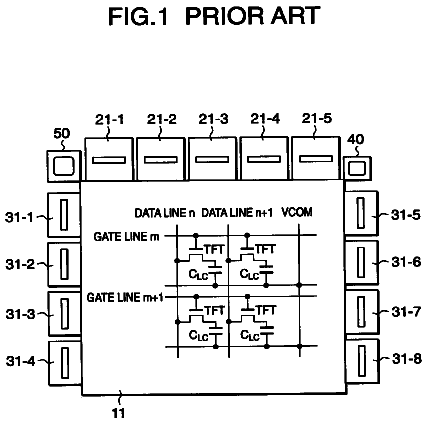
The configuration of the liquid crystal display apparatus according to the invention is described by using FIG. 1. FIG. 1 is a plan view illustrating the TFT array substrate in a liquid crystal display panel of the liquid crystal display apparatus. The TFT array substrate is used in an active matrix liquid crystal display apparatus. Reference numeral 1 designates a gate wiring, numeral 3 denotes a source wiring, numeral 11 designates a display region, numeral 12 denotes a picture frame region, numeral 30 denotes a control portion, numeral 31 designates a gate driver IC, numeral 32 denotes a source driver IC, and numeral 100 designates the TFT array substrate.
In the display region 11, the plural gate wirings 1 and the plural source wirings 3 are formed in such a way as to intersect with one another. The gate wirings 1 and the source wirings 3 are extended to the picture frame region serving as a nondisplay region. In the picture frame region 12 provided on the periphery of the display region 11, the gate driver ICs 31 and the source driver ICs 32 are connected to one another through, for example, an ACF. Moreover, on the TFT array substrate, plural gate driver ICs 31 are disposed at an end part of a side thereof, which is perpendicular to the gate wirings 1, and plural source driver ICs 32 are disposed at an end part of a side thereof, which is perpendicular to the source wirings 3. That is, the gate driver ICs 31 and the source driver ICs 32 are disposed on end parts of adjacent sides of the TFT array substrate 100, respectively. The plural gate driver ICs 31 are disposed along an end part of and along a side of the TFT array substrate 100. The plural source driver ICs 32 are disposed along an end part of and along a side adjoining the side, along which the gate driver ICs 31 are disposed, of the TFT array substrate 100.
A control portion 30 for supplying electric power and signals to each of the driver ICs is formed in the proximity of a corner portion at which the side provided with the gate driver ICs 31 intersects with the side provided with the source driver ICs 32. This control portion 30 is connected to each of the driver ICs put on the TFT array substrate 100 through wirings, such as FPC. The control portion 30 outputs digitalized display data (represented by, for instance, R, G, and B signals respectively associated with red, green, and blue) and various kinds of control signals to each of the driver ICs according to information sent from an external input apparatus, such as a personal computer. Each of the driver ICs is driven by the electric power sent from the control portion 30, and outputs a scanning signal or a display signal to the gate wiring 1 or the source wiring 3 according to the control signal and the display data sent from the control portion 30. Major control signals sent to the gate driver ICs 31 are vertical synchronization signals, gate driver clock signals, and so on. On the other hand, major control signals sent to the source driver ICs 32 are horizontal synchronization signals, start pulse signals, source driver clock signals, and so forth. Moreover, the control portion 30 outputs a gradation voltage, which is generated according to a reference voltage, to the source driver ICs 32. The source driver ICs 32 latch the inputted display data therein in a time sharing manner. Thereafter, a DA (digital to analog) conversion is performed in synchronization with the horizontal synchronization signal inputted from the control portion 30. Display signals are outputted to the source wiring 3 from output terminals of the source driver ICs 32 according to analog voltages obtained by this conversion.
A TFT (not shown) is formed in the vicinity of each of the intersections between the gate wirings 1 and the source wirings 3. Scanning signals are supplied to the gate wirings 1 in such a manner as to switch between on and off states of the TFT connected thereto. On the other hand, display signals for driving the liquid crystals are supplied to the source wirings 3. In a period during which the TFT is turned on, the source wiring 3 and the pixel electrode formed in each of the pixels are conducted to each other, so that the display signal is written to the pixel electrode. In a state in which the TFT is turned on, the pixel potential V.sub.s is inputted to the pixel electrode according to the display signal. On the other hand, the common potential V.sub.com is always supplied to the common electrode disposed opposite to the pixel electrode. The liquid crystal is driven by a driving voltage generated between the pixel electrode and the common electrode according to this display signal. The driving voltage is generated according to the difference between the pixel potential V.sub.s and the common potential V.sub.com. Concretely, the driving voltage is (V.sub.s-V.sub.com).
Among the plural gate wirings 1, the gate wirings, the associated TFT of each of which is turned on, are sequentially scanned from the top one thereof. Then, display signals are sequentially supplied to the source wirings 3, the TFT of each of which is turned on, in synchronization with the scanning of the gate wirings 1, the associated TFT of each of which is turned on. That is, display signals for the pixels are written thereto in a period during which the associated TFT is turned on. The display signal is supplied to the source wirings 3 so that the pixel potential V.sub.s is written to the gate wiring 1, the associated TFT of which is turned on. These scanning signals and display signals are supplied from the gate driver IC or the source driver IC 32.
A period of turning-on of TFTs connected to all the gate wirings is called a vertical period (or a vertical scanning period). Generally, a vertical scanning frequency is 60 Hz. That is, in a time period of ( 1/60) sec., the gate wirings are sequentially scanned from the top one to the bottom one thereof, so that the display signals are written to all the pixel electrodes. Therefore, the rewriting of the screen is performed 60 times per second. Furthermore, a period of turning-on of each of TFTs connected to the gate wirings is called a horizontal period (or a horizontal scanning period). A horizontal scanning frequency is given by multiplying (the frequency of the vertical period) by (the number of the gate wirings). Therefore, generally, a write time assigned to one gate wiring 1, that is, the horizontal period is given by dividing ( 1/60 sec.) by (the number of the gate wirings). Within a time allotted to this one gate wiring 1, the pixel potential V.sub.s is written to the pixel electrode associated with this gate wiring. The rewriting of the screen is performed by sequentially performing scanning on the gate wirings from the top one thereof. Then, when the writing is completed up to the bottom, the writing is repeatedly performed from the top again.
The configuration of a pixel, in which this TFT is formed, is described by using FIG. 2. FIG. 2 is a plan view illustrating the configuration, of a pixel in the IPS liquid crystal display apparatus.
In FIG. 2, reference numeral 3 designates a source wiring, which extends from an end portion of one pixel in a direction being nearly perpendicular to the direction of an electric field generated between the common electrode 5 (to be described later) and the pixel electrode 6. The film thickness of this source wiring 3 ranges, for instance, from 200 nm to 500 nm. Reference numeral 5 is a comb-like common electrode, which is constituted by plural electrodes disposed alternately in parallel to plural electrodes of the pixel electrode 6 (to be described later) and which is also called a counter electrode. The film thickness of this common electrode 5 is, for example, 100 nm. Reference numeral 6 denotes a comb-like pixel electrode that is constituted by plural electrodes, which are connected to a thin film transistor and provided in parallel to the source wiring 3, and that is made of metal, such as chrome (Cr), or formed of a transparent electrically conductive film made of ITO (Indium Tin Oxide). Reference numeral 7 designates a common capacitance wiring made of metal, such as chrome (Cr), and connected to the common electrode 5 through a through hole. In this example, each of the source wiring 3, the common electrode 5, and the pixel electrode 6 is bent once at the central portion thereof. Further, this inflection point is provided on the common capacitance wiring 7. Thus, with the configuration including bent electrodes, two directions can be obtained as the direction in which the liquid crystal is driven. Consequently, deterioration in viewing-angle characteristics, which would occur in a specific direction in an IPS liquid crystal panel, can be prevented.
As shown in FIG. 2, the source wiring 3 and the common electrode 5 provided between the pixels adjoining in a lateral direction that is the direction, in which an electric field is generated, overlap with each other. In, other words, the common electrode 5 is provided on the source wiring 3 in such a way as to wrap around the source wiring 3 through an insulating film 4 and an organic planarization film 9. A TFT 10 is formed in the vicinity of the intersection between the gate wiring 1 and the source wiring 3. This TFT 10 is turned on/off by a gate pulse of a scanning signal inputted to the gate wiring 1. In a state in which the TFT 10 is turned on, the source wiring 3 and the pixel electrode 6 are conducted to each other, and the pixel potential is written thereto.
A process of manufacturing the liquid crystal display apparatus, in which pixels shown in FIG. 2 are formed, is described by using FIGS. 3A to 3E. FIGS. 3A to 3E are process cross-sectional views illustrating a manufacturing process of the TFT array substrate. First, as shown in FIG. 3A, on an insulating substrate, a film made of Cr, Al, Ti, Ta, Mo, W, Ni, Cu, Au, Ag, or an alloy mainly consisting of these metals, or an electrically conductive transparent film, such as an ITO film, or a multilayer film consisting of these films is formed by a sputtering method or evaporation method, and subsequently, the gate wiring 1, a gate electrode, and a common capacitance wiring are formed thereon by photoengraving and processing. Then, as shown in FIG. 3B, the gate insulating film 2 made of silicon nitride or the like is formed. Moreover, a semiconductor film 93 made of an amorphous silicon, polycrystalline polysilicon or the like, alternatively, in the case of an n-TFT, a contact film made of n.sup.+-amorphous-silicon, n.sup.+-polycrystalline-polysilicon or the like heavily doped with impurities, such as P, is continuously formed by, for example, a plasma CVD method, an atmospheric CVD method, or a reduced-pressure CVD method. Subsequently, the contact film and the semiconductor film 93 are processed like islands.
Subsequently, as shown in FIG. 3C, a film made of Cr, Al, Ti, Ta, Mo, W, Ni, Cu, Au, Ag, or an alloy mainly consisting of these metals, or an electrically conductive transparent film, such as an ITO film, or a multilayer film consisting of these films is formed by a sputtering method or evaporation method. Then, the source wiring 3, a source electrode, a drain electrode and a retention volume electrode are formed thereon by photoengraving and by fine processing techniques. Furthermore, the contact film is etched and removed from a channel region by using the source electrode and the drain electrode or a photoresist, which is used for forming these electrodes, as a mask.
Then, the insulating film 4 made of an inorganic material, such as silicon nitride, oxide silicon, or the like or constituted by an organic film is formed. Thereafter, a contact hole is formed by photoengraving and by subsequently etching. The source wiring 3 or the gate wiring 1 is exposed by providing the contact hole. The insulating film 4 may be a laminated film constituted by the inorganic film and the organic film. Consequently, the configuration shown in FIG. 3D is obtained.
After a film made of Cr, Al, Ti, Ta, Mo, W, Ni, Cu, Au, Ag, or an alloy mainly consisting of these metals, or an electrically conductive transparent film, such as an ITO film, or a multilayer film consisting of these films is formed on the insulating film 4, as shown in FIG. 3E, the pixel electrode and the common electrode 5 are formed by patterning. Consequently, the common electrode can be formed on an opening portion of the organic planarization film 9 in a disconnection repairing region or on the laminated part.
The TFT array substrate 100 composing the IPS liquid crystal display apparatus according to this embodiment can be manufactured by the above process. Further, the liquid crystals are sandwiched between this TFT substrate 100 and the CF substrate disposed opposite thereto and bonded therebetween by a sealant. At that time, liquid crystal molecules are oriented at a predetermined angle by a rubbing method, an optical orientation method, or the like. Incidentally, any known methods may be employed as the method of orienting the liquid crystals. Additionally, the gate driver ICs 31, the source driver ICs 32, and the common capacitance power supplies are connected to the gate wirings, the source wirings, and the common capacitance wiring, respectively, to thereby manufacture the liquid crystal display apparatus.
In the configuration shown in FIG. 2, the source wirings 3 and the pixel electrodes 6 are formed so that each of the source wirings is close to the associated pixel electrode. According to the invention, to reduce an error electric field generated between the source wiring 3 and the pixel electrode of a pixel, which are disposed close to each other, at the writing in another pixel, the following signal processing is performed. This signal processing is described by using FIG. 4. FIG. 4 is a timing chart illustrating a scanning signal and a display signal.
In FIG. 4, reference character G designates a scanning signal to be inputted to the gate wiring, and character S denotes a display signal to be inputted to the source wiring. Also, reference character V.sub.com designates a common potential to be supplied to the common electrode, and character V.sub.s denotes a pixel potential to be written to the pixel electrode. FIG. 4 is drawn by focusing attention to a scanning signal for the single gate wiring 1 and to a display signal for the single source wiring.
A positive gate pulse is added to the gate wiring 1 selected as shown in FIG. 4. Consequently, the TFT is put into an ON-state. Thus, the writing of the pixel potential V.sub.s to the pixel electrode 6 is performed. That is, in a period in which the TFT is in an ON-sate, the level of a display signal is the pixel potential V.sub.s of an associated pixel. Also, the writing thereof to the pixel electrode is performed. Then, the liquid crystal is driven by an electric field generated between the pixel electrode 6 and the common electrode 5. That is, the electric potential difference (V.sub.s-V.sub.com) between the pixel potential V.sub.s and the common potential V.sub.com is used as a driving voltage. The liquid crystal is driven horizontally to the substrate according to this driving voltage. Incidentally, among the plural gate wirings 1, a gate pulse is inputted to the gate wiring, which is shifted in turn from the top one of the plural gate wirings by one horizontal period ("1H" shown in FIG. 4). Then, the writing of the pixel potential V.sub.s is sequentially performed on the pixel electrodes 6 of pixels each associated with the gate wiring to which the gate pulse is inputted.
The description continues in the full USPTO document.
 Lapsed, fee not paid7 drawings