Cross-reference to related applications
The disclosure of Japanese Patent Application No. 2010-259022 filed on Nov. 19, 2010 including the specification, drawings and abstract is incorporated herein by reference in its entirety.
Background
The present invention relates to a semiconductor device and a manufacturing method thereof, and particularly to a technology which is effective when applied to the manufacturing of a semiconductor element having a metal silicide layer.
With the increasing integration of semiconductor devices, a field effect transistor (MISFET: Metal Insulator Semiconductor Field Effect Transistor) has been scaled down according to a scaling rule. However, the resistances of a gate electrode and source/drain regions increase to result in the problem that, even when the field effect transistor is scaled down, a high-speed operation cannot be obtained. To solve the problem, a Salicide (Self Aligned Silicide) technique has been studied in which a low-resistance metal silicide layer such as, e.g., nickel silicide layer or cobalt silicide layer is formed by self-alignment over a surface of each of a conductive film forming the gate electrode and semiconductor regions forming the source/drain regions to thereby reduce the resistances of the gate electrode and the source/drain regions.
In Japanese Unexamined Patent Publication No. 2010-114449 (Patent Document 1), it is disclosed that a silicide layer containing NiSi (nickel monosilicide) and retaining phase stability and film stability even at a high temperature is formed over the main surface of a semiconductor substrate. It is also disclosed that the silicide layer described above contains, e.g., Pt (platinum) or the like.
Related art documents
Patent Documents
[Patent Document 1]
Japanese Unexamined Patent Publication No. 2010-114449 [Patent Document 2] Japanese Unexamined Patent Publication No. 2002-141504
Summary
As semiconductor devices have been scaled down, it has been required to reduce the film thickness of a silicide layer formed over the upper surface of each of the source/drain regions and gate electrodes of field-effect transistors. However, when the thickness of the silicide layer is reduced, the silicide layer is physically unstabilized and abnormally grows in the semiconductor substrate. As a result, in the semiconductor substrate under the gate electrodes, the silicide layers mainly containing NiSi.sub.2 are formed. In this case, a leakage defect resulting from a junction leakage current may increase to degrade the reliability of the semiconductor device, and therefore it is difficult to reduce the film thickness of the silicide layer.
In recent years, in a salicide process for forming a silicide layer, a metal film formed over a semiconductor substrate is caused to react with a part of a source region, a drain region, and a gate electrode to form the silicide layer. Accordingly, it is common practice to adopt a method which performs an anneal treatment (heat treatment) in two separate steps. In this case, in a 2nd anneal treatment as a second heat treatment, the semiconductor substrate is heated at temperature higher than that of a 1st anneal treatment as a first heat treatment.
However, when the second heat treatment is performed at a high temperature of about 500 to 600.degree. C. to form an extremely thin silicide layer having a film thickness of, e.g., not more than 14 nm, it is difficult to suppress abnormal growth of the silicide layer because of the excessively high temperature of the heat treatment. On the other hand, when the second heat treatment is performed using a lamp type or heat-conduction type anneal apparatus or the like, it is difficult to form a silicide layer with a uniform film thickness. Thus, when the film thickness of the silicide layer cannot be controlled accurately and abnormal growth of crystals (grains) in the silicide layer or the like occurs, a leakage current is likely to flow between the semiconductor substrate and the silicide layer, and so forth, resulting in the problem of the degraded junction leakage characteristic of the silicide layer.
In Japanese Unexamined Patent Publication No. 2002-141504 [Patent Document 2], it is disclosed that a heat treatment is performed at a temperature of not less than 850.degree. C. for a period of not more than 60 seconds using, e.g., a microwave anneal process to form a silicide layer. Here, it is stated that, by performing a first heat treatment using, e.g., the microwave anneal process or the like in the step of forming the silicide layer and subsequently performing a second heat treatment under the same conditions as or different conditions from those for the first heat treatment, the silicide layer can be activated. Thus, it is disclosed that the heat treatment using a microwave is performed also in the 1st anneal.
However, if the first heat treatment is to be performed using the microwave as shown in Patent Document 2, a problem arises that a junction leakage current in the silicide layer increases compared with that in the case where the first heat treatment is performed using a heat-conduction type anneal apparatus or the like. The reason for this is as follows, which has been found by the present inventors. That is, with the microwave, it may be occasionally difficult to uniformly heat the semiconductor substrate having a pure metal attached to the entire surface thereof. If the semiconductor substrate containing, e.g., silicon is directly heated with the microwave, abnormal growth of the silicide layer is more likely to occur due to a subsequent heat treatment, such as the second heat treatment or the step of forming interconnects, than in the case where the first heat treatment is performed by heating a metal film over the semiconductor substrate using a heat-conduction type anneal apparatus or the like.
An object of the present invention is to provide a technique for improving the junction leakage characteristic of a semiconductor device having a silicide layer.
The above and other objects and novel features of the present invention will become apparent from a statement in the present specification and the accompanying drawings.
The following is a brief description of the outline of a representative embodiment of the invention disclosed in the present application.
That is, a method of manufacturing a semiconductor device of the present invention includes the steps of: (a) preparing a semiconductor substrate; (b) forming a semiconductor region in the semiconductor substrate; (c) forming a metal film over the semiconductor substrate including the semiconductor region; (d) performing a first heat treatment to cause the metal film to selectively react with the semiconductor region and form a metal silicide layer over the semiconductor region; (e) after the step (d), removing an unreacted part of the metal film to leave the metal silicide layer over the semiconductor region; (f) after the step (e), performing a second heat treatment; and (g) after the step (f), forming an insulating film over the semiconductor substrate including the metal silicide layer. In the step (d), the first heat treatment is performed using a heat-conduction type anneal apparatus. In the step (f), the second heat treatment is performed using a microwave anneal apparatus.
The following is a brief description of an effect obtained according to the representative embodiment of the invention disclosed in the present application.
According to the representative embodiment, it is possible to improve the reliability of a semiconductor device having an element in which a metal silicide layer is formed over a surface of a semiconductor substrate.
Brief description of the drawings
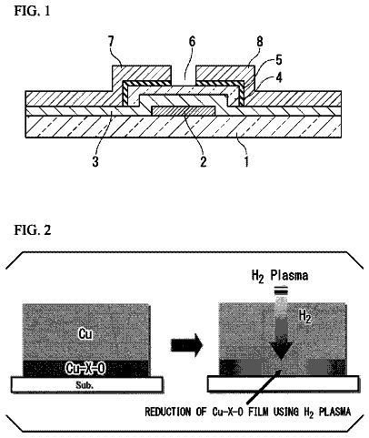
FIG. 1 is a main-portion cross-sectional view showing a semiconductor device as an embodiment of the present invention;
FIGS. 2(a) to 2(d) are tables showing Pt concentration distributions in the respective metal silicide layers of the semiconductor device as the embodiment of the present invention and a semiconductor device as a comparative example, of which FIG. 2(a) is the table showing the Pt concentration distribution in each of the metal silicide layers of an n-channel MISFET of the comparative example, FIG. 2(b) is the table showing the Pt concentration distribution in the metal silicide layer of a p-channel MISFET of the comparative example, FIG. 2(c) is the table showing the Pt concentration distribution in each of the metal silicide layers of an n-channel MISFET as the embodiment of the present invention, and FIG. 2(d) is the table showing the Pt concentration distribution in the metal silicide layer of a p-channel MISFET as the embodiment of the present invention;
FIG. 3 is a main-portion cross-sectional view of the semiconductor device as the embodiment of the present invention during a manufacturing step;
FIG. 4 is a main-portion cross-sectional view of the semiconductor device during a manufacturing step subsequent to that of FIG. 3;
FIG. 5 is a main-portion cross-sectional view of the semiconductor device during a manufacturing step subsequent to that of FIG. 4;
FIG. 6 is a main-portion cross-sectional view of the semiconductor device during a manufacturing step subsequent to that of FIG. 5;
FIG. 7 is a main-portion cross-sectional view of the semiconductor device during a manufacturing step subsequent to that of FIG. 6;
FIG. 8 is a main-portion cross-sectional view of the semiconductor device during a manufacturing step subsequent to that of FIG. 7;
FIG. 9 is a main-portion cross-sectional view of the semiconductor device during a manufacturing step subsequent to that of FIG. 8;
FIG. 10 is a main-portion cross-sectional view of the semiconductor device during a manufacturing step subsequent to that of FIG. 9;
FIG. 11 is a main-portion cross-sectional view of the semiconductor device during a manufacturing step subsequent to that of FIG. 10;
FIG. 12 is a main-portion cross-sectional view of the semiconductor device during a manufacturing step subsequent to that of FIG. 11;
FIG. 13 is a plan view showing a part of a heat-conduction type anneal apparatus in the embodiment of the present invention in cut-away relation;
FIG. 14 is a plan view showing a part of the heat-conductive type anneal apparatus in the embodiment of the present invention;
FIG. 15 is a cross-sectional view along the line A-A of FIG. 14;
FIG. 16 is a cross-sectional view showing a part of the heat-conduction type anneal apparatus in the embodiment of the present invention;
FIG. 17 is a cross-sectional view showing the heat-conduction type anneal apparatus;
FIG. 18 is a cross-sectional view showing a batch type anneal apparatus as a comparative example;
FIG. 19 is a cross-sectional view showing a lamp type anneal apparatus as another comparative example;
FIG. 20 is a cross-sectional view showing a microwave anneal apparatus;
FIG. 21 is a main-portion cross-sectional view of the semiconductor device during a manufacturing step subsequent to that of FIG. 12;
FIG. 22 is a main-portion cross-sectional view of the semiconductor device during a manufacturing step subsequent to that of FIG. 21;
FIG. 23 is a main-portion cross-sectional view of the semiconductor device during a manufacturing step subsequent to that of FIG. 22;
FIG. 24 is graphs each showing a relationship between the film thickness of a metal silicide layer and a junction leakage current;
FIG. 25 is graphs each showing a relationship between the temperature of a second heat treatment and the junction leakage current;
FIG. 26 is graphs each showing a cumulative frequency distribution of the junction leakage current in the semiconductor device;
FIG. 27 is graphs each showing a temperature at which the metal silicide layer is phase transformed;
FIG. 28 is graphs each showing the time of heating using the microwave anneal apparatus and the temperature of a semiconductor substrate;
FIG. 29 is graphs each showing a relationship between the temperature of a second heat treatment and the degree of segregation of Pt;
FIG. 30 is a main-portion cross-sectional view of a semiconductor device shown as a variation of the present embodiment;
FIG. 31 is graphs each showing the relationship between the width of the metal silicide layer and the sheet resistance of the metal silicide layer;
FIG. 32 is graphs each showing the relationship between the width of the metal silicide layer and the sheet resistance of the metal silicide layer;
FIG. 33 is graphs each showing the planarity of the interface between the metal silicide layer and the semiconductor substrate;
FIG. 34 is graphs each showing the planarity of the interface between the metal silicide layer and the semiconductor substrate; and
FIG. 35 is a main-portion cross-sectional view showing a semiconductor device as the comparative example.
Detailed description
Referring to the drawings, an embodiment of the present invention will be described below in detail. Note that, throughout all the drawings for illustrating the embodiment, members having the same functions are designated by the same reference numerals, and a repeated description thereof is omitted. Additionally, in the following embodiment, a description of the same or like parts will not be repeated in principle unless it is particularly necessary.
A semiconductor device of the present embodiment will be described with reference to FIGS. 1 and 2. FIG. 1 is a cross-sectional view of the semiconductor device in which MIS (Metal Insulator Semiconductor) type FETs (Field Effect Transistors) (hereinafter simply referred to as MISFETs) are formed over a semiconductor substrate 1.
As shown in FIG. 1, the main surface of the semiconductor substrate 1 has first regions and second regions which are separated by isolation regions 4 formed in the upper surface of the semiconductor substrate 1. In the main surface of the semiconductor substrate 1 in each of the first regions, a MISFET (p-channel MISFET Qp) having a p-type channel is formed. In the main surface of the semiconductor substrate 1 in each of the second regions, a MISFET (n-channel MISFET Qn) having an n-type channel is formed.
The p-channel MISFET Qp has a gate electrode 8b formed via a gate insulating film 7 over an n-type well 6 which is an n-type channel semiconductor layer obtained by introducing an n-type impurity (e.g., P (phosphorus)) into the main surface of the semiconductor substrate 1, and source/drain regions formed in the main surface of the semiconductor substrate 1 such that the n-type well 6 immediately under the gate electrode 8b is interposed therebetween. Over the both side walls of the gate electrode 8b formed of, e.g., a polysilicon film, sidewalls 11 each formed of a silicon oxide film or the like are formed. In the main surface of the semiconductor substrate 1 located under the sidewalls 11, p.sup.--type semiconductor regions 10a which are semiconductor regions into which a p-type impurity (e.g., B (boron)) has been introduced at a relatively low concentration are formed. In regions outward of the p.sup.--type semiconductor regions 10a with respect to a region immediately under the gate electrode 8b, i.e., in the main surface of the semiconductor substrate 1 located between the p.sup.--type semiconductor regions 10a and the isolation regions 4, p.sup.+-type semiconductor regions 10b into which a p-type impurity (e.g., B (boron)) has been introduced at a concentration higher than in the p.sup.--type semiconductor regions 10a are formed. The source/drain regions are formed of the p.sup.--type semiconductor regions 10a and the p.sup.+-type semiconductor regions 10b.
Likewise, the n-channel MISFET Qn has a gate electrode 8a formed via the gate insulating film 7 over a p-type well 5 which is a p-type channel semiconductor layer obtained by introducing a p-type impurity (e.g., B (boron)) into the main surface of the semiconductor substrate 1, and source/drain regions formed in the main surface of the semiconductor substrate 1 such that the p-type well 5 immediately under the gate electrode 8a is interposed therebetween. Over the both side walls of the gate electrode 8a formed of, e.g., a polysilicon film, the sidewalls are formed. In the main surface of the semiconductor substrate 1 located under the sidewalls 11, n.sup.--type semiconductor regions 9a which are semiconductor regions into which an n-type impurity (e.g., P (phosphorus)) has been introduced at a relatively low concentration are formed. In the main surface of the semiconductor substrate 1 located between the n.sup.--type semiconductor regions 9a and the isolation regions 4, n.sup.+-type semiconductor regions 9b into which an n-type impurity (e.g., P (phosphorus)) has been introduced at a concentration higher than in the n.sup.--type semiconductor regions 9a are formed. The source/drain regions are formed of the n.sup.--type semiconductor regions 9a and the n.sup.+-type semiconductor regions 9b.
Over the respective upper surfaces of the n.sup.+-type semiconductor regions 9b, the p.sup.+-type semiconductor regions 10b, and the gate electrodes 8a and 8b, metal silicide layers 41 each containing NiSi (mono-nickel silicide), which is a compound of Ni (nickel) and Si (silicon), and Pt (platinum) are formed. The main surface of the semiconductor substrate 1 including the re-channel MISFET Qn, the p-channel MISFET Qp, the metal silicide layers 41, the sidewalls 11, and the isolation regions 4 is covered with an insulating film 43 which is a thick interlayer insulating film via a thin insulating film 42 serving as an etching stopper film. From the upper surface of the insulating film 43 to the upper surfaces of the metal silicide layers 41, contact holes extend through the insulating film 43.
In the contact holes over the metal silicide layers 41, plugs 45 for supplying predetermined potentials to the n-channel MISFET Qn and the p-channel MISFET Qp are formed. The plugs 45 are coupling members mainly containing, e.g., W (tungsten). The metal silicide layers 41 are for reducing contact resistances between the plugs 45 each formed of a metal material such as tungsten and the semiconductor substrate 1 mainly formed of silicon and ohmically coupling the plugs 45 to the n.sup.+-type semiconductor regions 9b and p.sup.+-type semiconductor regions 10b of the source/drain regions and to the gate electrodes 8a and 8b.
Over the insulating film 43 and the plugs 45, an insulating film 52 serving as an interlayer insulating film is formed via a stopper insulating film 51. In the insulating film 52, a plurality of interconnect trenches 53 exposing the upper surfaces of the plugs 45 are formed. In the interconnect trenches 53, interconnects 55 for supplying the predetermined potentials to the n-channel MISFET Qn and the p-channel MISFET Qp are buried via barrier conductor films 54. Note that the barrier conductor films 54 are barrier films for preventing Cu (copper) mainly contained in the interconnects 55 from being diffused into the insulating films 52 and 43 or the like. Note that the contact holes immediately over the gate electrodes 8a and 8b, the plugs 45, and the interconnects 55 are not shown in FIG. 1 since they are not formed in the regions shown in FIG. 1, but are formed in other regions.
A characteristic feature of the semiconductor device of the present embodiment is that each of the metal silicide layers contains Pt (platinum) and, at the bottom surface of the metal silicide layer 41, i.e., at the interface between the metal silicide layer 41 and the semiconductor substrate 1, the concentration of Pt is higher in the p-channel MISFET Qp than in the n-channel MISFET Qn. Conversely, at the upper surface of the metal silicide layer 41, the concentration of Pt is higher in the n-channel MISFET Qn than in the p-channel MISFET Qp. That is, in each of the metal silicide layers 41 of the re-channel MISFET Qn, Pt is present (segregated) in a larger amount at the upper surface thereof than at the bottom surface thereof. On the other hand, in each of the metal silicide layers 41 of the p-channel MISFET Qp, Pt is present (segregated) in a larger amount at the bottom surface thereof than at the upper surface thereof. Note that the segregation mentioned herein indicates a state where a material such as, e.g., Pt is diffused concentrically into a specified region of a certain structure and present at a density higher than in the other region of the foregoing structure or a state where the density of the material in a region of a certain structure is higher than in an equivalent region of another structure as a comparison target.
The metal silicide layer 41 having such a Pt distribution is formed by performing two heat treatments which are performed when the metal silicide layers 41 are formed such that, e.g., a heat-conduction type anneal apparatus, not a microwave anneal apparatus, is used for the first heat treatment (1st anneal treatment) and the microwave anneal apparatus is used for the second heat treatment (2nd anneal treatment), as will be described later. Note that the microwave anneal apparatus, the heat-conduction type anneal apparatus, and other anneal apparatus will be described later.
As will be described later in detail, when the first heat treatment is performed using, e.g., the heat-conduction type anneal apparatus, not the microwave anneal apparatus, and the second heat treatment is performed using the microwave anneal apparatus, a junction leakage current in the metal silicide layer 41 can be reduced compared with the case where the first heat treatment is performed using the microwave anneal apparatus or where the second heat treatment is performed using a lamp type anneal apparatus or the heat-conduction type anneal apparatus. This is because, by using the heat-conduction type anneal apparatus or the like, not the microwave anneal apparatus, for the first heat treatment and using the microwave anneal apparatus for the second heat treatment to form the metal silicide layer 41 as described above, it is possible to prevent abnormal growth of the metal silicide layer and accurately control the film thickness of the extremely thin metal silicide layer 41.
In addition, the p-channel MISFET Qp has a characteristic such that, when Pt in the metal silicide layers 41 is segregated at the interfaces between the metal silicide layers 41 and the semiconductor substrate 1, the contact resistances between the metal silicide layers 41 and the semiconductor substrate 1 decrease to improve the performance of the semiconductor device. Conversely, the n-channel MISFET Qn has a characteristic such that, when Pt in the metal silicide layers 41 is segregated at the interfaces between the metal silicide layers 41 and the semiconductor substrate 1, the contact resistances between the metal silicide layers 41 and the semiconductor substrate 1 increase to degrade the performance of the semiconductor device. That is, in the p-channel MISFET Qp, it is preferable to cause Pt to be segregated in a larger amount at the bottom surfaces of the metal silicide layers 41 while, in the n-channel MISFET Qn, it is preferable to cause Pt to be segregated in a larger amount in the upper portions of the metal silicide layers 41 than at the bottom surfaces thereof.
When the microwave anneal apparatus is used in the first heat treatment or when the lamp type anneal apparatus or heat-conduction type anneal apparatus is used in the second heat treatment, in each of the p-channel MISFET Qp and the n-channel MISFET Qn, Pt is segregated in the upper surfaces of the metal silicide layers 41. This causes no problem in the n-channel MISFET Qn, but causes the problem of increased contact resistances between the semiconductor substrate 1 and the metal silicide layers 41 in the p-channel MISFET Qp.
Here, FIGS. 2(a) to 2(d) show tables showing ratios among the respective amounts of Ni (nickel), Si (silicon), and Pt (platinum) in the metal silicide layers. FIG. 2(a) is the table showing a Pt concentration distribution in each of the metal silicide layers of an n-channel MISFET as a comparative example. FIG. 2(b) is the table showing the Pt concentration distribution in the metal silicide layer of a p-channel MISFET as the comparative example. FIG. 2(c) is the table showing the Pt concentration distribution in each of the metal silicide layers of an n-channel MISFET as the present embodiment. FIG. 2(d) is the table showing the Pt concentration distribution in the metal silicide layer of a p-channel MISFET as the present embodiment.
Of the four tables shown in FIGS. 2(a) to 2(d), the uppermost table (FIG. 2(a)) shows the ratio among the respective amounts of Ni, Si, and Pt in each of the upper layer (top), middle layer (middle), and lower layer (bottom) of the metal silicide layer of the n-channel MISFET (NMIS) formed by performing each of the first and second heat treatments using the heat-conduction type anneal apparatus. There are also shown a ratio (Pt/Ni) of Pt to Ni and a ratio (Pt/Si) of Pt to Si in each of the upper layer, middle layer, and lower layer of the metal silicide layer. The second uppermost table (FIG. 2(b)) of FIGS. 2(a) to 2(d) shows the ratio among the respective amounts of Ni, Si, and Pt in each of the upper layer, middle layer, and lower layer of the metal silicide layer of the p-channel MISFET (PMIS) formed under the same conditions as in the table of FIG. 2(a), the ratio of Pt to Ni therein, and the ratio of Pt to Si therein.
By contrast, the third uppermost table (FIG. 2(c)) of FIGS. 2(a) to 2(d) shows the ratio among the respective amounts of Ni, Si, and Pt in each of the upper layer, middle layer, and lower layer of the metal silicide layer of the n-channel MISFET (NMIS) formed using the heat-conduction type anneal apparatus in the first heat treatment and performing a microwave anneal treatment (MWA: Microwave Annealing) as the second heat treatment in the present embodiment, the ratio of Pt to Ni therein, and the ratio of Pt to Si therein. The lowermost table (FIG. 2(d)) of FIGS. 2(a) to 2(d) shows the ratio among the respective amounts of Ni, Si, and Pt in each of the upper layer, middle layer, and lower layer of the metal silicide layer of the p-channel MISFET (PMIS) of the present embodiment formed under the same conditions as in the table of FIG. 2(c), the ratio of Pt to Ni therein, and the ratio of Pt to Si therein.
That is, the tables shown in FIGS. 2(a) and 2(b) are for illustrating element distributions in the metal silicide layers of a semiconductor device as the comparative example, while the tables shown in FIGS. 2(c) and 2(d) are for illustrating element distributions in the metal silicide layers of the semiconductor device of the present embodiment.
As can be seen from FIGS. 2(a) to 2(d), in the metal silicide layers in the tables of FIGS. 2(a) and 2(b) as the comparative example, Pt (platinum) is segregated in the upper layers of the metal silicide layers. By contrast, as shown in the table of FIG. 2(c), the metal silicide layer of the re-channel MISFET of the present embodiment has the Pt distribution having substantially the same tendency as that of the comparative example shown in the table of FIG. 2(a). However, in the metal silicide layer of the p-channel MISFET of the present embodiment shown in FIG. 2(d), Pt is distributed such that the Pt concentration tends to increase with increasing distance from the upper layer of the metal silicide layer toward the lower layer thereof, which is different from the tendency of the comparative example shown in the table of FIG. 2(b). That is, it can be said that Pt (platinum) in the metal silicide layer of the p-channel MISFET is segregated in a larger amount in the bottom portion of the metal silicide layer than in the comparative example.
That is, as can be seen from FIGS. 2(c) and 2(d), in the silicide layer of the p-channel MISFET, the ratio of Pt to Si increases with increasing distance from the upper surface thereof toward the bottom surface thereof and, in the silicide layer of the n-channel MISFET, the ratio of Pt to Si decreases with increasing distance from the upper surface thereof toward the bottom surface thereof.
It can also be seen from the tables shown in FIGS. 2(a) to 2(d) that, in the upper surface and bottom surface of the metal silicide layer of the p-channel MISFET and in the middle layer therebetween, Si and Pt are contained in substantially the same proportion and, in each of the metal silicide layers of the re-channel MISFETs, the ratio of Pt to Si decreases with increasing distance from the upper surface thereof toward the bottom surface thereof.
By thus performing the first heat treatment using the heat-conduction type anneal apparatus, not the microwave anneal apparatus, and performing the second heat treatment using the microwave anneal apparatus to form the metal silicide layers 41, it is possible to cause Pt in each of the metal silicide layers of the p-channel MISFET Qp to be segregated in a larger amount at the bottom surface (at the interface with the semiconductor substrate 1) of the metal silicide layer 41. Also, for the same reason, it is possible to cause Pt in each of the metal silicide layers 41 of the n-channel MISFET Qn to be segregated in a larger amount not at the bottom surface of the metal silicide layer 41, but at the upper surface thereof. This allows a reduction in the contact resistance between the metal silicide layer 41 and the semiconductor substrate 1 in each of the p-channel MISFET Qp and the n-channel MISFET Qn and therefore allows an improvement in the performance of the semiconductor device.
Next, manufacturing steps of the semiconductor device of the present embodiment will be described with reference to the drawings. FIGS. 3 to 10 are main-portion cross-sectional views of a semiconductor device as an embodiment of the present invention, e.g., a semiconductor device having a CMISFET (Complementary MISET).
First, as shown in FIG. 3, the semiconductor substrate (semiconductor wafer) 1 formed of p-type single-crystal silicon having a specific resistance of, e.g., about 1 to 10 .OMEGA.cm or the like is prepared. Then, the semiconductor substrate 1 is thermally oxidized to form an insulating film 2 having a thickness of, e.g., about 11 nm over the surface thereof. Thereafter, an upper-layer insulating film 3 having a thickness of, e.g., about 90 nm is deposited thereover by a CVD (Chemical Vapor Deposition) method or the like. The insulating film 2 is formed of a silicon oxide or the like, while the insulating film 3 is formed of a silicon nitride film or the like. Then, as shown in FIG. 4, using a photoresist pattern (not shown) as an etching mask, the insulating film 3, the insulating film 2, and the semiconductor substrate 1 are successively dry-etched to form trenches (trenches for isolation) 4a each having a depth of, e.g., about 300 nm in the semiconductor substrate 1 in regions where the isolations are to be formed. The trenches 4a are for isolation, i.e., for forming the isolation regions 4, which will be described later.
Next, as shown in FIG. 5, an insulating film 4b having a thickness of, e.g., about 10 nm is formed over the main surface of the semiconductor substrate 1 including the insides (side walls and bottom portions) of the trenches 4a. Then, over the main surface of the semiconductor substrate 1, to fill up the trenches 4a, an insulating film 4c is formed (deposited) by a CVD method or the like.
The insulating film 4b is formed of a silicon oxide film or a silicon oxynitride film. When the insulating film 4b is the silicon oxynitride film, an effect is obtained which allows the prevention of volume expansion resulting from the oxidation of the side walls of the trenches 4a by a heat treatment subsequent to the step of forming the insulating film 4b and allows a reduction in compressive stress acting on the semiconductor substrate 1.
The insulating film 4c is a silicon oxide film deposited by a HDP-CVD (High Density Plasma CVD) method, an O.sub.3-TEOS oxide film, or the like. Note that the O.sub.3-TEOS oxide film is a silicon oxide film formed by a thermal CVD method using O.sub.3 (ozone) and TEOS (Tetraethoxysilane or Tetra Ethyl Ortho Silicate) as a raw material gas (source gas).
Then, by subjecting the semiconductor substrate 1 to a heat treatment at, e.g., about 115.degree. C..degree., the insulating film 4c buried in the trenches 4a is baked. In a state prior to baking, the silicon oxide film deposited by the HDP-CVD method is denser than the O.sub.3-TEOS oxide film. Therefore, when the insulating film 4c is the O.sub.3-TEOS oxide film, the insulating film 4c shrinks due to baking to achieve the effect of allowing a reduction in the compressive stress acting on the semiconductor substrate 1. On the other hand, when the insulating film 4c is the silicon oxide film deposited by the HDP-CVD method, the shrinkage of the insulating film 4c during the baking is smaller in amount than when the insulating film 4c is the O.sub.3-TEOS oxide film so that the compressive stress exerted on the semiconductor substrate 1 by the isolation regions 4 increases.
Next, as shown in FIG. 6, the insulating film 4c is polished by a CMP (Chemical Mechanical Polishing) method to expose the insulating film 3. After the insulating film 3 is removed by wet etching using a hot phosphoric acid or the like, the insulating film 4c and the insulating film 2 outside the trenches 4a are removed using HF or the like to leave the insulating films 4b and 4c in the trenches 4a, thereby forming the isolation regions (isolations) 4.
In this manner, the isolation regions 4 formed of the insulating films 4b and 4c buried in the trenches 4a are formed. In the present embodiment, the isolation regions 4 are preferably formed not by a LOCOS (Local Oxidization of Silicon) method, but by a STI (Shallow Trench Isolation) method. That is, each of the isolation regions 4 of the present embodiment is preferably formed of an insulator (which is the insulating films 4b and 4c herein) buried in the trenches 4a for isolation formed in the semiconductor substrate 1. The n-channel MISFET Qn (i.e., the gate insulating film 7, the gate electrode 8a, and the n.sup.--type semiconductor regions 9a and the n.sup.+-type semiconductor regions 9b for the source/drain regions each forming the re-channel MISFET Qn), which will be described later, is formed in an active region defined (surrounded) by the isolation region 4. Also, the p-channel MISFET Qp (i.e., the gate insulating film 7, the gate electrode 8b, and the p.sup.--type semiconductor regions 10a and the p.sup.+-type semiconductor regions 10b for the source/drain regions each forming the p-channel MISFET Qp), which will be described later, is also formed in an active region defined (surrounded) by the isolation region 4.
Next, as shown in FIG. 7, the p-type well 5 and the n-type well 6 are each formed at a predetermined depth from the main surface of the semiconductor substrate 1. The p-type well 5 can be formed by, e.g., ion-implanting a p-type impurity such as boron (B) into the semiconductor substrate 1 in a region where the n-channel MISFET is to be formed using a photoresist film (not shown) covering a region where the p-channel MISFET is to be formed as an ion implantation stopping mask, and so forth. On the other hand, the n-type well 6 can be formed by, e.g., ion-implanting an n-type impurity such as phosphorus (P) or arsenic (As) into the semiconductor substrate 1 in the region where the p-channel MISFET is to be formed using another photoresist film (not shown) covering the region where the re-channel MISFET is to be formed as an ion implantation stopping mask, and so forth.
Next, by wet etching using, e.g., an aqueous hydrofluoric (HF) acid solution or the like, the surface of the semiconductor substrate 1 is purified (cleaned). Then, over the surface (i.e., the surfaces of the p-type well 5 and the n-type well 6) of the semiconductor substrate 1, the gate insulating film 7 is formed. The gate insulating film 7 is formed of, e.g., a thin silicon oxide film or the like, and can be formed by, e.g., a thermal oxidization method or the like.
Next, over the semiconductor substrate 1 (i.e., over the gate insulating film 7 of the p-type well 5 and the n-type well 6), as a conductive film for forming the gate electrodes, a silicon film 8 such as a polysilicon film is formed. Of the silicon film 8, the region where the n-channel MISFET is to be formed (region which is to serve as the gate electrode 8a described later) is changed to a low-resistance n-type semiconductor film (doped polysilicon film) by ion-implanting an n-type impurity such as phosphorus (P) or arsenic (As) using a photoresist film (not shown) as a mask, and so forth. Of the silicon film 8, the region where the p-channel MISFET is to be formed (region which is to serve as the gate electrode 8b described later) is changed to a low-resistance p-type semiconductor film (doped polysilicon film) by ion-implanting a p-type impurity such as boron (B) using another photoresist film (not shown) as a mask, and so forth. The silicon film 8 may also be formed by depositing an amorphous silicon film, and then changing the deposited amorphous silicon film into a polysilicon film by a heat treatment after film deposition (after ion implantation).
Next, as shown in FIG. 8, the silicon film 8 is patterned using a photolithographic method and a dry etching method to form the gate electrodes 8a and 8b.
The gate electrode 8a serving as the gate electrode of the n-channel MISFET is formed of polysilicon (an n-type semiconductor film or a doped polysilicon film) into which an n-type impurity has been introduced, and formed over the p-type well 5 via the gate insulating film 7. That is, the gate electrode 8a is formed over the gate insulating film 7 of the p-type well 5. On the other hand, the gate electrode 8b serving as the gate electrode of the p-channel MISFET is formed of polysilicon (a p-type semiconductor film or a doped polysilicon film) into which a p-type impurity has been introduced, and formed over the n-type well 6 via the gate insulating film 7. That is, the gate electrode 8b is formed over the gate insulating film 7 of the n-type well 6. The gate lengths of the gate electrodes 8a and 8b can be changed as necessary to, e.g., about 50 nm.
Next, as shown in FIG. 9, into the regions of the p-type well 5 located on both sides of the gate electrode 8a, an n-type impurity such as phosphorus (P) or arsenic (As) is ion-implanted to form the (pair of) n.sup.--type semiconductor regions 9a. Also, into the regions of the n-type well 6 located on both sides of the gate electrode 8b, a p-type impurity such as boron (B) is ion-implanted to form the (pair of) p.sup.--type semiconductor regions 10a. The depths (junction depths) of the n.sup.--type semiconductor regions 9a and the p.sup.--type semiconductor regions 10a can be set to, e.g., about 30 nm.
Next, over the side walls of the gate electrodes 8a and 8b, the sidewall spacers or sidewalls (side-wall insulating films) each formed of, e.g., silicon oxide, silicon nitride, a laminate film of the insulating films thereof, or the like are formed as insulating films. The sidewalls 11 can be formed by, e.g., depositing a silicon oxide film, a silicon nitride film, or a laminate film thereof over the semiconductor substrate 1 and anisotropically etching the silicon oxide film, the silicon nitride film, or the laminate film thereof by an RIE (Reactive Ion Etching) method or the like.
The description continues in the full USPTO document.
 Lapsed, fee not paid5 drawings