 Lapsed, fee not paid27 drawings
Chips & Semiconductors · US 8,791,446 B2
Semiconductor device
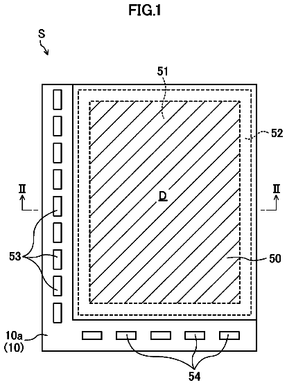
According to one embodiment, a semiconductor device includes a substrate and an interconnect region on the substrate.
US 8,791,469 B2 · Assignee: Toyoda Gosei Co., Ltd. · Inventors: Shinohara; Hironao et al.
Sheet 1 of 14 from the published document. All sheets in the USPTO PDF
In a semiconductor light emitting element (1) having a sapphire substrate (100), and lower (210) and upper (220) semiconductor layers laminated on the sapphire substrate, the substrate includes a substrate top surface (113), a substrate bottom surface (114), first substrate side surfaces (111) and second substrate side surfaces (112); plural first (121a) and second (122a) cutouts are provided at a border between the first substrate side surface, the second substrate side surface and the substrate top surface; the lower semiconductor layer includes a lower semiconductor bottom surface, a lower semiconductor top surface (213), first lower semiconductor side surfaces (211) and second lower semiconductor side surfaces (212); plural first projecting portions (211a) and plural first depressing portions (211b) are provided on the first lower semiconductor side surface; and plural second protruding portions (212a) and second flat portions (212b) are provided on the second lower semiconductor side surface.
There is known a semiconductor light emitting element, in which a semiconductor layer including an n-type semiconductor layer, a light emitting layer and a p-type semiconductor layer that are composed of a group III nitride semiconductor or the like is laminated on a substrate composed of sapphire single crystal or the like. In such a semiconductor light emitting element, there exists a technique for suppressing multiple reflections of light within the semiconductor layer and improving light extraction efficiency in the semiconductor light emitting element by providing projections and depressions on a side surface of the semiconductor layer to cause light emitted from the light emitting layer to be irregularly reflected by the projections and depressions (refer to Patent Document 1).
1 of 14 drawing sheets so far from the published document, cropped to the drawing. Every sheet is in the USPTO PDF.
What the patent claimed, word for word. All of it is now free to use.
The present invention relates to a semiconductor light emitting element, a method for producing the light emitting element and a light emitting device.
There is known a semiconductor light emitting element, in which a semiconductor layer including an n-type semiconductor layer, a light emitting layer and a p-type semiconductor layer that are composed of a group III nitride semiconductor or the like is laminated on a substrate composed of sapphire single crystal or the like.
In such a semiconductor light emitting element, there exists a technique for suppressing multiple reflections of light within the semiconductor layer and improving light extraction efficiency in the semiconductor light emitting element by providing projections and depressions on a side surface of the semiconductor layer to cause light emitted from the light emitting layer to be irregularly reflected by the projections and depressions (refer to Patent Document 1).
Patent Literature
Patent Document 1: Japanese Patent Application Laid-Open Publication No. 2004-6662
Technical Problem
However, in the semiconductor light emitting element, in addition to the case of providing the projections and depressions on the side surface of the semiconductor layer, it is required to further improve the light extraction efficiency.
The present invention has an object to improve light extraction efficiency in a semiconductor light emitting element including a substrate.
Solution to Problem
A semiconductor light emitting element to which the present invention is applied is a semiconductor light emitting element having a substrate and a semiconductor layer, which includes a light emitting layer that emits light by current flow and is laminated on the substrate. The substrate includes a substrate top surface on which the semiconductor layer is laminated, a substrate bottom surface provided on an opposite side of the substrate top surface, and a substrate side surface formed to enclose limbs of the substrate top surface and the substrate bottom surface, and is provided with plural cutouts, which are formed by cutting out a part of the substrate and are arranged at intervals along a border between the substrate top surface and the substrate side surface; the semiconductor layer includes a semiconductor bottom surface provided in contact with the substrate top surface, a semiconductor top surface provided on an opposite side of the semiconductor bottom surface, and a semiconductor side surface provided to enclose limbs of the semiconductor bottom surface and the semiconductor top surface; and on the semiconductor side surface, projections and depressions are formed by arranging plural depressing portions, each of which extends from a semiconductor bottom surface side toward a semiconductor top surface side, and depresses toward an inside of the semiconductor layer.
Here, the semiconductor layer has a first semiconductor layer provided between the substrate and the light emitting layer, and a second semiconductor layer that includes the light emitting layer and is provided on the first semiconductor layer, and the plural depressing portions are provided in a region where the first semiconductor layer of the semiconductor side surface is exposed.
Moreover, the semiconductor side surface is provided to be inclined with respect to a direction vertical to the substrate top surface.
Further, an angle formed by the semiconductor bottom surface and the semiconductor side surface is larger than 90 degrees.
Then, a horizontal cross-sectional shape of the depressing portion is different between the semiconductor bottom surface side and the semiconductor top surface side.
Moreover, a curvature of the depressing portion on the semiconductor bottom surface side is smaller than a curvature of the depressing portion on the semiconductor top surface side.
Further, a curvature of the depressing portion on the semiconductor bottom surface side is substantially equal to a curvature of the depressing portion on the semiconductor top surface side, and a central axis of the depressing portion is different between the semiconductor bottom surface side and the semiconductor top surface side.
Then, in the semiconductor side surface, the projections and depressions are formed larger on the semiconductor top surface side in the semiconductor side surface than on the semiconductor bottom surface side in the semiconductor side surface.
Moreover, the substrate side surface includes a first substrate side surface along a first direction and a second substrate side surface along a second direction intersecting the first direction, the plural cutouts are arranged along the first direction with first intervals at a border between the substrate top surface and the first substrate side surface, and the plural cutouts are arranged along the second direction with second intervals at a border between the substrate top surface and the second substrate side surface, the semiconductor side surface includes a first semiconductor side surface along the first direction and a second semiconductor side surface along the second direction, on the first semiconductor side surface, the plural depressing portions are arranged, each of which corresponds to each of the plural cutouts arranged at the border between the substrate top surface and the first substrate side surface, on the second semiconductor side surface, the plural depressing portions are arranged, each of which corresponds to each of the plural cutouts arranged at the border between the substrate top surface and the second substrate side surface, and the depressing portions arranged on the first semiconductor side surface and the depressing portions arranged on the second semiconductor side surface are different in shape.
Further, projections and depressions are formed on the substrate top surface.
From another viewpoint, a method for producing a semiconductor light emitting element, to which the present invention is applied, includes: a laser irradiation process that sequentially irradiates a semiconductor lamination substrate, in which a semiconductor layer including a light emitting layer that emits light by current flow is laminated on a top surface of a substrate having the top surface and a bottom surface provided on an opposite side of the top surface, with laser light from a side where the semiconductor layer is laminated, to thereby form plural openings, each of which penetrates the semiconductor layer and is formed by cutting out a part of the substrate, arranged with an interval to the adjacent opening; an etching process that applies wet etching to the semiconductor layer in the semiconductor lamination substrate, in which the plural openings are formed; and a dividing process that divides the semiconductor lamination substrate along an arrangement of the plural openings.
Here, in the etching process, the wet etching is applied to the semiconductor layer so that the adjacent openings are united together.
Moreover, prior to the laser irradiation process, a protecting film forming process that forms a protecting film on the semiconductor layer is further included, and in the laser irradiation process, the semiconductor lamination substrate, on which the protecting film is formed, is irradiated with laser light from a side where the protecting film is formed so that the laser light reaches the top surface of the substrate through the protecting film and the semiconductor layer, and in the etching process, the wet etching is applied to the semiconductor layer in the semiconductor lamination substrate with the protecting film being formed on the semiconductor layer.
Further, the laser irradiation process includes: a first laser irradiation process that sequentially irradiates the semiconductor lamination substrate, in which the semiconductor layer containing a group III nitride is laminated on the top surface configured with a C-plane of a sapphire single crystal, with laser light in a first direction along an M-plane of the sapphire single crystal, to thereby form the plural openings arranged with first intervals along the first direction; and a second laser irradiation process that sequentially irradiates the semiconductor lamination substrate with laser light in a second direction intersecting the first direction, to thereby form the plural openings arranged with second intervals along the second direction.
Then, a semiconductor laminating process that laminates the semiconductor layer on the top surface of the substrate, on which a process for forming projections and depressions is applied, to thereby form the semiconductor lamination substrate is further included.
From another viewpoint, a light emitting device, to which the present invention is applied, includes a semiconductor light emitting element having a substrate and a semiconductor layer, which includes a light emitting layer that emits light by passing a current and is laminated on the substrate; and an electrical power supply member that supplies electrical power to the semiconductor light emitting element, wherein the substrate includes a substrate top surface on which the semiconductor layer is laminated, a substrate bottom surface provided on an opposite side of the substrate top surface and a substrate side surface formed to enclose limbs of the substrate top surface and the substrate bottom surface, and is provided with plural cutouts, which are formed by cutting out a part of the substrate and are arranged at intervals along a border between the substrate top surface and the substrate side surface, the semiconductor layer includes a semiconductor bottom surface provided in contact with the substrate top surface, a semiconductor top surface provided on an opposite side of the semiconductor bottom surface and a semiconductor side surface provided to enclose limbs of the semiconductor bottom surface and the semiconductor top surface, and the semiconductor side surface includes plural depressing portions, each of which extends from a semiconductor bottom surface side toward a semiconductor top surface side, and depresses toward an inside of the semiconductor layer.
Here, an angle formed by the semiconductor bottom surface and the semiconductor side surface is larger than 90 degrees, and the semiconductor light emitting element extracts light from the semiconductor top surface side in the semiconductor layer.
Advantageous Effects of Invention
According to the present invention, it is possible to improve the light extraction efficiency in the semiconductor light emitting element including the substrate.
FIG. 1 is an example of a perspective view of a semiconductor light emitting element to which the exemplary embodiment is applied;
FIG. 2 is an example of a top view of the semiconductor light emitting element shown in FIG. 1;
FIG. 3 is an example of a vertical cross-sectional view of a sapphire substrate and a laminated semiconductor layer in the exemplary embodiment;
FIGS. 4A to 4D are examples of a vertical cross-sectional view of the semiconductor light emitting element to which the exemplary embodiment is applied;
FIGS. 5A to 5D are examples of a horizontal cross-sectional view of the semiconductor light emitting element to which the exemplary embodiment is applied;
FIG. 6 is an example of a cross-sectional view of a light emitting device to which the semiconductor light emitting element according to the exemplary embodiment is applied;
FIG. 7 is a flowchart showing an example of a method for producing the semiconductor light emitting element;
FIG. 8 is a schematic view indicating a relation between a crystal orientation of the sapphire substrate and a crystal orientation of the laminated semiconductor layer formed on the sapphire substrate;
FIGS. 9A and 9B are diagrams showing an example of a configuration of an element-group formation substrate obtained by performing an element-group forming process;
FIGS. 10A and 10B are top views showing an example of a configuration of the element-group formation substrate after forming first irradiation lines and second irradiation lines obtained by performing a surface laser process;
FIGS. 11A to 11D are vertical cross-sectional views showing an example of a configuration of the element-group formation substrate after forming first irradiation lines and second irradiation lines obtained by performing a surface laser process;
FIGS. 12A to 12C are schematic views illustrating a relation between an etching time in the etching process and changes in shapes of first opening portions and the first irradiation line;
FIG. 13 is an example of a top view of a semiconductor light emitting element in an exemplary embodiment 2;
FIGS. 14A and 14B are schematic views for illustrating a shape of a first lower semiconductor side surface of the semiconductor light emitting element in an exemplary embodiment 1 and the exemplary embodiment 2.
Hereinafter, exemplary embodiments according to the present invention will be described in detail with reference to accompanying drawings. It should be noted that there are some cases where a size or a thickness of each component in the drawings that are referred to in the description below is different from a dimension of an actual semiconductor light emitting element or the like.
Exemplary Embodiment 1
(Configuration of Semiconductor Light Emitting Element)
FIG. 1 is an example of a perspective view of a semiconductor light emitting element 1 to which this exemplary embodiment is applied, and FIG. 2 is an example of a top view of the semiconductor light emitting element 1 shown in FIG. 1.
As shown in FIGS. 1 and 2, the semiconductor light emitting element 1 of the exemplary embodiment includes: a sapphire substrate 100 as an example of a substrate; a laminated semiconductor layer 200 laminated on the sapphire substrate 100 as an example of a semiconductor layer; and a p-electrode 300 and an n-electrode 400 formed on the laminated semiconductor layer 200. In addition, the laminated semiconductor layer 200 of the exemplary embodiment includes a lower semiconductor layer 210 laminated on the sapphire substrate 100 as an example of a first semiconductor layer and an upper semiconductor layer 220 laminated on the lower semiconductor layer 210 as an example of a second semiconductor layer. It should be noted that, in this specific example, the p-electrode 300 is formed on the upper semiconductor layer 220 and the n-electrode 400 is formed on the lower semiconductor layer 210.
Moreover, as shown in FIG. 1, the semiconductor light emitting element 1 of the exemplary embodiment has a shape that is substantially a rectangular parallelepiped. Then, as shown in FIG. 2, the semiconductor light emitting element 1 has substantially a rectangle shape including long sides and short sides in a case of being viewed from a side where the p-electrode 300 and the n-electrode 400 are formed.
In the exemplary embodiment, in the case where the semiconductor light emitting element 1 is viewed from the side where the p-electrode 300 and the n-electrode 400 are formed, a direction along the long sides is regarded as a first direction x and a direction along the short sides is regarded as a second direction y. Moreover, a direction that is perpendicular to the first direction x and the second direction y, and proceeds from the sapphire substrate 100 side toward the laminated semiconductor layer 200 side within the semiconductor light emitting element 1 is regarded as a third direction z.
Further, as shown in FIG. 1, the sapphire substrate 100 of the exemplary embodiment has a shape that is substantially a rectangular parallelepiped. Then, as shown in FIG. 2, the sapphire substrate 100 has substantially a rectangle shape including long sides along the first direction x and short sides along the second direction y in a case of being viewed from a side where the laminated semiconductor layer 200 is laminated. Consequently, the sapphire substrate 100 includes four substrate side surfaces, a substrate top surface 113 on which the laminated semiconductor layer 200 is laminated, and a substrate bottom surface 114 facing the substrate top surface 113 via the four substrate side surfaces (refer to FIG. 3 to be described later). Then, each of the substrate top surface 113 and the substrate bottom surface 114 has a rectangular shape including two long sides along the first direction x and two short sides along the second direction y.
Moreover, in the exemplary embodiment, of the four substrate side surfaces, each of two substrate side surfaces on the two long sides along the first direction x is referred to as a first substrate side surface 111, and each of two substrate side surfaces on the two short sides along the second direction y is referred to as a second substrate side surface 112.
In this specific example, as the sapphire substrate 100, a sapphire single crystal in which a C-plane is assumed to be the substrate top surface 113 is used. It should be noted that, as a plane direction of the substrate top surface 113, it is desirable to use the C-plane of a sapphire single crystal that is likely to obtain the laminated semiconductor layer 200 with good quality. Then, as the substrate top surface 113, it is further desirable to use a plane that is provided with a minute off angle with respect to the C-plane of the sapphire single crystal. In the case of providing the off angle, 1 degree or less is applied as the off angle. In the exemplary embodiment, it is simply said that the substrate top surface 113 is a C-plane, including the case where the off angle is provided. Further, the sapphire single crystal used as the sapphire substrate 100 may contain trace amounts of impurities.
Further, each of the two first substrate side surfaces 111 in the sapphire substrate 100 is provided along an M-plane of the sapphire single crystal used as the sapphire substrate 100, and each of the two second substrate side surfaces 112 is provided along an A-plane of the sapphire single crystal. In other words, in the exemplary embodiment, the first direction x is a direction along the M-plane of the sapphire single crystal, and the second direction y is a direction along the A-plane of the sapphire single crystal.
It should be noted that, as a substrate for growing the laminated semiconductor layer 200, other than the sapphire substrate 100 composed of the sapphire single crystal, SiC single crystal substrate may be used.
Moreover, as shown in FIGS. 1 and 2, the lower semiconductor layer 210 of the exemplary embodiment has a shape that is substantially a rectangular parallelepiped. Accordingly, the lower semiconductor layer 210 includes: four lower semiconductor side surfaces; a lower semiconductor top surface 213 on which the upper semiconductor layer 220 and the n-electrode 400 are laminated; and a lower semiconductor bottom surface 214, as an example of a semiconductor bottom surface, that faces the lower semiconductor top surface 213 via the four lower semiconductor side surfaces and contacts the substrate top surface 113. In the exemplary embodiment, of the four lower semiconductor side surfaces in the lower semiconductor layer 210, each of two lower semiconductor side surfaces along the first direction x is referred to as a first lower semiconductor side surface 211, and each of two lower semiconductor side surfaces along the second direction y is referred to as a second lower semiconductor side surface 212.
Here, in the exemplary embodiment, the area of the lower semiconductor bottom surface 214 in the lower semiconductor layer 210 is formed smaller than the area of the substrate top surface 113 in the sapphire substrate 100. Consequently, the limb (or peripheral edge) portion 115 in the substrate top surface 113 of the sapphire substrate 100 is exposed to the outside.
In addition, in this specific example, the area of the lower semiconductor bottom surface 214 is formed smaller than the area of the lower semiconductor top surface 213 in the lower semiconductor layer 210.
Further, as shown in FIGS. 1 and 2, the upper semiconductor layer 220 of the exemplary embodiment has a shape that is substantially a rectangular parallelepiped. Accordingly, the upper semiconductor layer 220 includes: four upper semiconductor side surfaces; an upper semiconductor top surface 223, as an example of a semiconductor top surface, on which the p-electrode 300 is laminated; and an upper semiconductor bottom surface (not shown) that faces the upper semiconductor top surface 223 via the four upper semiconductor side surfaces and contacts the lower semiconductor top surface 213 in the lower semiconductor layer 210. In the exemplary embodiment, of the four upper semiconductor side surfaces in the upper semiconductor layer 220, each of two upper semiconductor side surfaces along the first direction x is referred to as a first upper semiconductor side surface 221, and each of two upper semiconductor side surfaces along the second direction y is referred to as a second upper semiconductor side surface 222. It should be noted that one second upper semiconductor side surface 222 of the two second upper semiconductor side surfaces 222 has a portion that curves like an arc along the n-electrode 400 provided on the lower semiconductor layer 210.
In the exemplary embodiment, each of the two first upper semiconductor side surfaces 221 and the two second upper semiconductor side surfaces 222 are provided substantially vertical to the lower semiconductor top surface 213 in the lower semiconductor layer 210 (also refer to FIGS. 4A to 4D to be described later).
Here, in the exemplary embodiment, the area of the upper semiconductor bottom surface in the upper semiconductor layer 220 is formed smaller than the area of the lower semiconductor top surface 213 in the lower semiconductor layer 210. Consequently, the limb portion in the lower semiconductor top surface 213 of the lower semiconductor layer 210 is exposed to the outside.
It should be noted that the semiconductor side surfaces are constituted by the first lower semiconductor side surfaces 211, the second lower semiconductor side surfaces 212, the first upper semiconductor side surfaces 221 and the second upper semiconductor side surfaces 222. Moreover, first semiconductor side surfaces are constituted by the first lower semiconductor side surfaces 211 and the first upper semiconductor side surfaces 221, and second semiconductor side surfaces are constituted by the second lower semiconductor side surfaces 212 and the second upper semiconductor side surfaces 222.
In the sapphire substrate 100 of the exemplary embodiment, a first cutout row 121 is formed along the first direction x at a border portion between the first substrate side surface 111 and the substrate top surface 113. The first cutout row 121 is, at the border portion between the first substrate side surface 111 and the substrate top surface 113, configured by plural first cutouts 121a, as an example of cutouts that are formed by cutting out a part of the sapphire substrate 100, arranged along the first direction x. Here, a distance between the adjacent first cutouts 121a is a first pitch p1.
Similarly, in the sapphire substrate 100 of the exemplary embodiment, a second cutout row 122 is formed along the second direction y at a border portion between the second substrate side surface 112 and the substrate top surface 113. The second cutout row 122 is, at the border portion between the second substrate side surface 112 and the substrate top surface 113, configured by plural second cutouts 122a, as an example of the cutouts that are formed by cutting out a part of the sapphire substrate 100, arranged along the second direction y. Here, a distance between the adjacent second cutouts 122a is a second pitch p2.
In addition, the depth of the first cutouts 121a and the second cutouts 122a is in the range of 0.1 .mu.m to 20 .mu.m.
It should be noted that, in the exemplary embodiment, the first pitch p1 and the second pitch p2 are equal (p1=p2).
Moreover, the first lower semiconductor side surface 211 in the lower semiconductor layer 210 of the exemplary embodiment includes plural first depressing portions 211b that extend along the third direction z and depress toward the inside of the lower semiconductor layer 210 and plural first projecting portions 211a that extend along the third direction z and project toward the outside of the lower semiconductor layer 210 compared to the first depressing portions 211b. Then, the plural first depressing portions 211b and the plural first projecting portions 211a are alternately arranged along the first direction x, and thereby a shape of depressions and projections that periodically changes along the first direction x is formed on the first lower semiconductor side surface 211. Here, in this specific example, a distance between the adjacent first projecting portions 211a is the first pitch p1.
Further, the second lower semiconductor side surface 212 in the lower semiconductor layer 210 of the exemplary embodiment is provided with second flat portions 212b that are formed substantially flat along the second direction y and the third direction z, and plural second protruding portions 212a that are provided on the upper semiconductor layer 220 side of the second flat portions 212b, protruding toward the outside of the lower semiconductor layer 210 compared to the second flat portions 212b, and arranged along the second direction. Then, on the second lower semiconductor side surface 212, a shape of depressions and projections that periodically changes along the second direction y is formed by the first protruding portions 212a and the second flat portions 212b. Here, a distance between the adjacent second protruding portions 212a is the second pitch p2.
It should be noted that, in the exemplary embodiment, depressing portions are configured with the first depressing portions 211b in the first lower semiconductor side surface 211 and the second flat portions 212b in the second lower semiconductor side surface 212.
In the exemplary embodiment, the projections and depressions formed in the first lower semiconductor side surface 211 and the projections and depressions formed in the second lower semiconductor side surface 212 are different in shape.
The shape of the projections and depressions in the first lower semiconductor side surface 211 and second lower semiconductor side surface 212 in the lower semiconductor layer 210 will be described in detail in a later stage.
It should be noted that, in this specific example, the shape of projections and depressions is not formed on the first upper semiconductor side surface 221 and the second upper semiconductor side surface 222 in the upper semiconductor layer 220 including an n-cladding layer 203b, a light emitting layer 204 and a p-type semiconductor layer 205.
Subsequently, a laminated structure of the sapphire substrate 100 and the laminated semiconductor layer 200 in the semiconductor light emitting element 1 of the exemplary embodiment will be described.
FIG. 3 is an example of a vertical cross-sectional view of the sapphire substrate 100 and the laminated semiconductor layer 200 in the exemplary embodiment. It should be noted that, in the exemplary embodiment, a cross section along the direction vertical to the substrate top surface 113 of the sapphire substrate 100 is referred to as a vertical cross section, and a cross section along the direction in parallel with the substrate top surface 113 is referred to as a horizontal cross section.
As shown in FIG. 3, in the sapphire substrate 100 of the exemplary embodiment, plural projecting portions 113a projecting toward the laminated semiconductor layer 200 side are formed on the flat substrate top surface 113. The width of each projecting portion 113a is preferably 0.05 .mu.m to 5 .mu.m, and the height of each projecting portion 113a is preferably in the range of 0.05 .mu.m to 5 .mu.m. In addition, it is preferable that the pitch between the adjacent projecting portions 113a is smaller than the first pitch p1 (refer to FIG. 2) and the second pitch p2 (refer to FIG. 2).
It should be noted that, though the projecting portions 113a are not necessarily provided on the substrate top surface 113 of the sapphire substrate 100; however, from the viewpoint for improving crystallinity of the laminated semiconductor layer 200 laminated on the sapphire substrate 100 and light extraction efficiency of the semiconductor light emitting element 1, it is preferable to provide the plural projecting portions 113a on the substrate top surface 113. Further, from the viewpoint of forming the projections and depressions on the first lower semiconductor side surface 211 and the second lower semiconductor side surface 212 of the lower semiconductor layer 210, it is preferable to provide the plural projecting portions 113a on the substrate top surface 113 of the sapphire substrate 100.
Moreover, as shown in FIG. 3, the laminated semiconductor layer 200 in the exemplary embodiment is laminated on the substrate top surface 113 of the sapphire substrate 100 and on the projecting portions 113a formed on the substrate top surface 113.
Then, the laminated semiconductor layer 200 of the exemplary embodiment includes: an intermediate layer 201 laminated on the sapphire substrate 100; a base layer 202 laminated on the intermediate layer 201; the n-type semiconductor layer 203 laminated on the base layer 202; the light emitting layer 204 laminated on the n-type semiconductor layer 203; and the p-type semiconductor layer 205 laminated on the light emitting layer 204. It should be noted that other layers such as a transparent conductive layer and a protecting layer may be laminated on the p-type semiconductor layer 205. In the exemplary embodiment, those including the layers such as the transparent conductive layer and the protecting layer laminated on the p-type semiconductor layer 205 are referred to as the laminated semiconductor layer 200.
The n-type semiconductor layer 203 is configured with the n-contact layer 203a laminated on the base layer 202 and the n-cladding layer 203b laminated on the n-contact layer 203a. It should be noted that the n-contact layer 203a can also serve as the n-cladding layer 203b.
Moreover, the p-type semiconductor layer 205 is configured with a p-cladding layer 205a laminated on the light emitting layer 204 and a p-contact layer 205b laminated on the p-cladding layer 205a. It should be noted that the p-contact layer 205b can also serve as the p-cladding layer 205a.
It should be noted that, in the exemplary embodiment, the lower semiconductor layer 210 is configured with the intermediate layer 201, the base layer 202 and a part of the n-contact layer 203a on the base layer 202 side. Further, the upper semiconductor layer 220 is configured with a part of the n-contact layer 203a on the n-cladding layer 203b side, the n-cladding layer 203b, the light emitting layer 204, the p-cladding layer 205a and the p-contact layer 205b.
Subsequently, each layer constituting the laminated semiconductor layer 200 will be described.
It should be noted that, in the following description, AlGaN, GaN and GaInN are described with the compositional ratio of each element being omitted in some cases.
<Intermediate Layer>
The intermediate layer 201 mediates the difference in lattice constant between the sapphire substrate 100 and the base layer 202, and in particular, in the case where the sapphire substrate 100 is configured with a sapphire single crystal in which the C-plane is a principal plane, has a function of facilitating the formation of a single crystal layer which is c-axis oriented on a
plane (C-plane) of the sapphire substrate 100. Consequently, by forming the intermediate layer 201, it is possible to improve crystallinity of the base layer 202 to be laminated thereon.
The intermediate layer 201 of the exemplary embodiment is formed of AlN. It should be noted that, as the intermediate layer 201, other than AlN, those composed of polycrystal Al.sub.xGa.sub.1-xN (0.ltoreq.x.ltoreq.1) or single crystal Al.sub.xGa.sub.1-xN (0.ltoreq.x.ltoreq.1) may be used.
The thickness of the intermediate layer 201 is preferably in the range of 0.01 .mu.m to 0.5 .mu.m. If the thickness of the intermediate layer 201 is less than 0.01 .mu.m, there are some cases where an effect of the intermediate layer 201 to mediate the difference in lattice constant between the sapphire substrate 100 and the base layer 202 cannot be sufficiently obtained. Moreover, if the thickness of the intermediate layer 201 is more than 0.5 .mu.m, there is a possibility that the time of forming process of the intermediate layer 201 becomes longer though there is no change to the function of the intermediate layer 201, and accordingly the productivity is decreased.
<Base Layer>
As the base layer 202, Al.sub.xGa.sub.yIn.sub.zN (0.ltoreq.x.ltoreq.1, 0.ltoreq.y.ltoreq.1, 0.ltoreq.z.ltoreq.1, x+y+z=1) can be used.
The thickness of the base layer 202 is preferably 0.1 .mu.m or more, more preferably 0.5 .mu.m or more, and most preferably 1 .mu.m or more. The base layer 202 having good crystallinity is likely to be obtained by setting the thickness of the base layer 202 to be 1 .mu.m or more.
Moreover, to improve the crystallinity of the base layer 202, it is desirable that the base layer 202 is not doped with impurities. However, in the case where conductivity of p-type or n-type is needed, acceptor impurities or donor impurities can be added.
Further, for causing the first lower semiconductor side surface 211 (refer to FIG. 1) and the second lower semiconductor side surface 212 (refer to FIG. 1) to be inclined with respect to the direction vertical to the lower semiconductor bottom surface 214 and to be in different shapes of projections and depressions between the lower semiconductor top surface 213 side and the lower semiconductor bottom surface 214 side, it is desirable that the material of the intermediate layer 201 and the material of the base layer 202 are different. By difference between the material of the intermediate layer 201 and the material of the base layer 202, in an etching process (refer to FIG. 7) in the method for producing the semiconductor light emitting element to be described later, an etching shape and easiness in etching of the lower semiconductor layer 210 are likely to become different between the lower semiconductor top surface 213 side and the lower semiconductor bottom surface 214 side. As suitable examples of the intermediate layer 201 and the base layer 202, a material containing AlGaN can be used as the intermediate layer 201 and a material containing GaN and InGaN can be used as the base layer 202. In addition, a dopant may be added to the intermediate layer 201 or the base layer 202. In this case, it is desirable to change the kinds or a doping amount of the dopant to be added between the intermediate layer 201 and the base layer 202.
<N-Contact Layer>
The n-contact layer 203a is a layer for providing the n-electrode 400.
The n-contact layer 203a is preferably configured with the Al.sub.xGa.sub.1-xN layer (0.ltoreq.x<1, more preferably 0.ltoreq.x.ltoreq.0.5, and still more preferably 0.ltoreq.x.ltoreq.0.1).
Further, the n-contact layer 203a is preferably doped with n-type impurities. It is preferable to contain the n-type impurities having a concentration of 1.times.10.sup.17/cm.sup.3 to 1.times.10.sup.20/cm.sup.3, and a concentration of 1.times.10.sup.18/cm.sup.3 to 1.times.10.sup.19/cm.sup.3 is more preferable on the point that a good ohmic contact with the n-electrode 400 can be maintained. As the n-type impurities, Si, Ge, Sn and so on are provided, and Si and Ge are preferably provided.
The thickness of the n-contact layer 203a is preferably set to 0.5 .mu.m to 5 .mu.m, and more preferably set in the range of 1 .mu.m to 3 .mu.m. If the thickness of the n-contact layer 203a is in the above-described ranges, crystallinity of the light emitting layer 204 or the like is suitably maintained. Moreover, if the thickness of the n-contact layer 203a is in the above-described ranges, electrical resistance is reduced, to thereby produce an effect of reducing an operation voltage (VF). It should be noted that the case where the thickness of the n-contact layer 203a is excessively thick will lead to decrease of productivity.
<N-Cladding Layer>
The n-cladding layer 203b performs injection of the carriers into the light emitting layer 204 and confinement of the carriers.
The n-cladding layer 203b can be formed of AlGaN, GaN, GaInN and so on. The hetero junction of these structures or the superlattice structure, in which the layer is laminated plural times, may also be used. In the case where the n-cladding layer 203b is formed of GaInN, the band gap thereof is preferably larger than that of GaInN of the light emitting layer 204.
The n-type impurity concentration of the n-cladding layer 203b is preferably in the range of 1.times.10.sup.17/cm.sup.3 to 1.times.10.sup.20/cm.sup.3, and more preferably in the range of 1.times.10.sup.18/cm.sup.3 to 1.times.10.sup.19/cm.sup.3. It is preferable to provide the impurity concentration in these ranges in terms of maintaining excellent crystallinity and reducing operation voltage of the element.
The thickness of the n-cladding layer 203b is preferably in the range of 5 nm to 500 nm, and more preferably in the range of 50 nm to 200 nm.
It should be noted that, in the case where the n-cladding layer 203b is a layer containing the superlattice structure, the layer may contain a structure in which an n-side first layer composed of the group III nitride semiconductor with a thickness of 10 nm or less and an n-side second layer composed of the group III nitride semiconductor having a composition different from that of the n-side first layer and having a thickness of 10 nm or less are laminated.
Moreover, the n-cladding layer 203b may contain a structure in which the n-side first layers and the n-side second layers are alternately and repeatedly laminated, and in this case, the structure is preferably an alternating structure of GaInN and GaN or an alternating structure of GaInN having different compositions.
<Light Emitting Layer>
As the light emitting layer 204 to be laminated on the n-cladding layer 203b, a single quantum well structure or a multiple quantum well structure can be employed.
As a well layer having a quantum well structure, the group III nitride semiconductor layer composed of Ga.sub.1-yIn.sub.yN (0<y<0.4) that has been adjusted to be able to obtain desirable light emission wavelength is usually used. Moreover, in the case of employing the light emitting layer 204 having the multiple quantum well structure, the above-described Ga.sub.1-yIn.sub.yN is employed as the well layer, and Al.sub.zGa.sub.1-zN (0.ltoreq.z<0.3) having a band gap energy larger than that of the well layer is employed as a barrier layer. The well layer and the barrier layer may be doped or not doped with impurities depending upon a design thereof.
<P-Cladding Layer>
The p-cladding layer 205a performs confinement of carriers within the light emitting layer 204 and injection of carriers.
As the p-cladding layer 205a, there is no particular limitation as long as the band gap energy of the composition thereof is larger than that of the light emitting layer 204 and carriers can be confined within the light emitting layer 204, but, for example, Al.sub.xGa.sub.1-xN (0<x.ltoreq.0.4) is desirably used. It is preferable that the p-cladding layer 205a is composed of such AlGaN in terms of confinement of carriers within the light emitting layer 204.
The description continues in the full USPTO document.
About 6,344 words. The USPTO PDF has it with every drawing.
Fees are due 3.5, 7.5 and 11.5 years after grant. This patent expired on July 29, 2026, so the fee marked "not paid" was the one that went unpaid.
SEMICONDUCTOR LIGHT EMITTING ELEMENT, METHOD FOR PRODUCING SEMICONDUCTOR LIGHT EMITTING ELEMENT AND LIGHT EMITTING DEVICE
Filed Dec 2012 · published Jul 2013Semiconductor light emitting element having a plurality of substrate cutouts and semiconductor layer side surface projections
Filed Dec 2012 · granted Jul 2014Earlier publications, parents and continuations. None of them can still be enforced, or this patent would not be listed.
Prior art cited by the examiner or applicant. Useful when you check your own idea for novelty.
Everything on this page comes from the documents linked above.