Background of the invention
1. Field of the invention
The present invention relates to a control method for acquiring signals from photoelectric conversion elements and obtaining an image, an imaging apparatus that performs such control, and a radiation imaging system.
2. Description of the related art
In recent years, in a field of a digital X-ray imaging apparatus, in place of an image intensifier, an image sensor having a large area in which photoelectric conversion elements are arranged in a matrix has become popular. Compared to the image intensifier, the image sensor can improve resolution of an image, reduce distortion of an image, and downsize a volume of the imaging apparatus. Image sensors include image sensors of an amorphous silicon type, a charge coupled device (CCD) type, and a complementary metal-oxide semiconductor (CMOS) type.
In the above described image sensor, since noise enters elements included in a circuit, signals need to be extracted corresponding to an amount of received light while the noise is being removed. According to U.S. Pat. No. 6,950,132, a circuit is provided that applies reset potential to a light signal line and a noise signal line disposed between a circuit holding outputs of image pixels and a differential amplifier. By clamping a reset state generated by the reset potential at a subsequent stage of the differential amplifier, the noise of the differential amplifier can be removed.
In a period when the signals are not read from the pixels, a column signal line connected to a scanning line and a row signal line serving as an output line of an image circuit are set to a floating state. Since the signal lines on an element substrate have a certain capacity, the noise is superimposed on the signal lines, which results in an adverse effect on image quality.
Further, since the noise varies within a certain range over time, each of the images includes a different amount of noise superimposed thereon. According to the technique described in U.S. Pat. No. 6,950,132, in which a circuit for applying the reset potential to the signal line and a clamp circuit disposed at a subsequent stage of the signal line are separately required, a circuit structure becomes complicated.
Summary of the invention
According to an aspect of the present invention, an imaging apparatus includes a plurality of pixel circuits each having a pixel, a photoelectric conversion element and a sample hold circuit, a plurality of signal lines configured to read from the plurality of pixel circuits an electrical signal held in the sample hold circuit therein, control unit for performing a first control for applying the held electrical signal to the plurality of signal lines and a second control for sequentially applying to the signal lines the electrical signal obtained by each pixel circuit corresponding to light received by each of the plurality of pixels and reading the electrical signal, after the first control has been performed, and generation unit configured to not create image data based on the electrical signal applied to the signal line by the first control and to create image data based on the electrical signal read via the signal line by the second control.
Further features and aspects of the present invention will become apparent from the following detailed description of embodiments with reference to the attached drawings.
Brief description of the drawings
The accompanying drawings, which are incorporated in and constitute a part of the specification, illustrate embodiments, features, and aspects of the invention and, together with the description, serve to explain the principles of the invention.
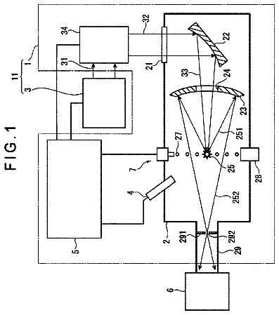
FIG. 1 illustrates a configuration of a radiation imaging system 1.
FIG. 2 illustrates a pixel circuit that is two-dimensionally formed on a rectangular semiconductor substrate.
FIG. 3 schematically illustrates an internal configuration of a rectangular semiconductor substrate.
FIG. 4 is a timing chart illustrating drive control when a moving image is captured in which an X-ray window is limited at a fixed frame rate.
FIG. 5 is a time chart for reading image data of three tiled rectangular semiconductor substrates using one analog/digital (A/D) converter.
FIG. 6 is a timing chart illustrating drive control of a sensor when a moving image is captured in which an X-ray window is limited at a fixed frame rate by an external synchronization mode.
FIG. 7 is a time chart of an initial potential applying operation by internal scanning of a reading circuit.
FIG. 8A is a circuit diagram of a pixel addition circuit in an image sensor of a CMOS type, and FIG. 8B illustrates a schematic configuration thereof.
FIG. 9 is a timing chart illustrating another example of drive control of a sensor when a moving image is captured in which an X-ray window is limited at a fixed frame rate by an external synchronization mode.
FIG. 10 is a time chart illustrating an example in which sampling drive patterns of sampling drive S2 are used for potential initializing processing of a reading circuit.
FIG. 11 is a timing chart illustrating drive control in a continuous X-ray fluoroscopic mode.
FIG. 12 is a timing chart illustrating another example of drive control in an external synchronization imaging mode.
FIG. 13 is a timing chart illustrating another example of drive control in an external synchronization imaging mode.
FIG. 14 is a time chart illustrating an example in which horizontal scanning of an initial potential applying operation by internal scanning of a reading circuit is performed while vertical scanning is being performed.
Description of the embodiments
Various embodiments, features, and aspects of the present technique will be described in detail below with reference to the drawings.
A first embodiment will be described below. A flat panel sensor 105 digital-converts three tiled rectangular semiconductor substrates as one conversion region of an A/D converter 108. A conversion clock of the A/D converter 108 for reading the rectangular semiconductor substrates is defined as 20 MHz. The A/D converter 108 performs A/D conversion on one line of the rectangular semiconductor substrates within the one A/D conversion region formed of three rectangular semiconductor substrates in a lateral direction while switching chip selection. The A/D converter 108 repeatedly performs the conversion sequentially from an outside portion to a center portion in a longitudinal direction.
A configuration of a radiation imaging system according to the first embodiment will be described based on FIG. 1. The radiation imaging system 10 includes a radioactive imaging device 100, an information processing device 101 that performs image processing and system control, an image display device 102, an X-ray generation device 103, and an X-ray tube 104.
The information processing device 101 synchronizes and controls the radioactive imaging device 100 and the X-ray generation device 103 in imaging an object. The radioactive imaging device 100 converts radiation that has gone through the object into visible light by a scintillator (not illustrated), and then image data created by photoelectrical conversion is transferred from the radioactive imaging device 100 to the information processing device 101. After the information processing device 101 performs image processing on the image data, the image display device 102 displays a radiation image of the object. Since irradiating the object with the radiation, generating the image, and displaying the image are repeatedly performed in real time, radioactive moving images of the object can be observed while the object image is being captured.
The flat panel sensor 105 in the radioactive imaging device 100 is a two-dimensional image sensor. A rectangular semiconductor substrate 106 is an image sensor of a CMOS type obtained by cutting out a two-dimensional photoelectric conversion element having a rectangular-strip shape from a silicon semiconductor wafer. The flat panel sensor 105 is obtained by tiling the rectangular semiconductor substrates 106 in the matrix of 12 columns.times.2 rows on a flat-face base plate (not illustrated).
On the rectangular semiconductor substrate 106 cut out in a rectangular-strip shape having about 20 mm of width and about 140 mm of length, 128 pixels and 896 pixels are arranged in a lateral direction and a longitudinal direction respectively with a pitch of 160 .mu.m. The rectangular semiconductor substrate 106 is developed as an area sensor for bonding, and the photoelectric conversion pixels generated on the rectangular semiconductor substrate 106 are two-dimensionally aligned at an even pitch. On the adjacent rectangular semiconductor substrates on the flat-face base plate, the photoelectric conversion elements are tiled across a boundary between the rectangular semiconductor substrates with the same pitch as that on the photoelectric conversion elements on the rectangular semiconductor substrate.
With this arrangement, the pixels are arranged in the matrix over the flat panel sensor 105. At an upper side portion and a lower side portion of the flat panel sensor 105, external terminals (electrode pads) (not illustrated) of the rectangular semiconductor substrates arranged in the matrix are aligned in one line. The electrode pad of the rectangular semiconductor substrate is connected with an external circuit by a printing wiring plate of a flying lead type (not illustrated).
On the rectangular semiconductor substrate, switching elements including an analog switch element for switching "Enable/Disable" of analog output are provided. By providing the switching elements for the analog output, output of the rectangular semiconductor substrate can be controlled by a chip selection control signal, and thus analog output lines on the rectangular semiconductor substrate can be collectively connected to an amplifier directly.
An imaging control unit 109 transmits/receives a control command and a synchronization signal to/from the information processing device 101 and transmits image data to the information processing device 101. Further, the imaging control unit 109 also has a function for controlling the flat panel sensor 105, which is an image sensor, to drive and control the flat panel sensor and control an imaging mode.
Furthermore, the imaging control unit 109 synthesizes frame data and digital image data for each block that has been A/D converted by a plurality of A/D converting devices included in the radioactive imaging device 100 to create the radiation image. Thus, the imaging control unit 109 also functions as an image generation unit and performs the aforementioned processing using the image creation circuit (not illustrated). The imaging control unit 109 transfers the radiation image to the information processing device 101.
Based on the control by the information processing device 101 and the imaging control unit 109, the information processing device 101 transmits/receives information to/from the imaging control unit 109 via an interface 110. The information processing device 101 transmits settings of the imaging mode to the imaging control unit 109, various parameters, start and finish of imaging. The imaging control unit 109 transmits to the information processing device 101 a state of a radioactive imaging device.
Main data will be described below. The captured image data is transmitted from the imaging control unit 109 to the information processing device 101. A READY signal 112 is used by the imaging control unit 109 to notify the information processing device 101 that the radioactive imaging device 100 is ready for imaging. When the information processing device 101 receives the READY signal 112 from the imaging control unit 109, an external synchronization signal 113 notifies the imaging control unit 109 of timing for exposing to the X-ray. An exposure permission signal 114 notifies that the radioactive imaging device 100 has finished preparing for imaging.
The exposure permission signal 114 is transmitted from the information processing device 101 to the X-ray generation device 103 while it is in a state of "Enable", the X-ray radiated from the X-ray tube 104 is stored as the valid X ray to create an X-ray image.
A configuration of the pixel circuit of the flat panel sensor 105 in the aforementioned radioactive imaging device 100 will be described based on FIG. 2. In FIG. 2, photo diode (PD) converts light into electricity. A reset switch M2 is a reset metal-oxide semiconductor (MOS) transistor (reset circuit) for discharging charge stored in floating diffusion capacitor Cfd.
The floating diffusion capacitor Cfd is a capacitor of floating diffusion (floating diffusion region) for storing the charge. The photoelectric conversion element storing the charge is formed by the PD, a parasite capacity of the PD and the floating diffusion capacitor Cfd. A sensitivity switch M1 is a sensitivity switching MOS transistor for switching between a high dynamic range mode and a high sensitivity mode.
A capacitor C1 is used to expand the dynamic range. When turning on the sensitivity switch M1, the charge can be stored. When turning on the sensitivity switch M1, the capacitance of the floating node portion is substantially increased and the dynamic range can be expanded, although the sensitivity becomes low. Thus, for example, when fluoroscopic imaging that needs high sensitivity is performed, the sensitivity switch M1 is turned off. When digital substraction angiography (DSA) imaging that needs a high dynamic range is performed, the sensitivity switch M1 is turned on.
A pixel amplifier M4 is an amplification MOS transistor operating as a source follower. A selection switch M3 is a selection MOS transistor switching the pixel amplifier M4 to an operation state. The pixel amplifier M4 generates signal voltage corresponding to signal charge stored in the floating diffusion capacitor Cfd.
A subsequent stage of the pixel amplifier M4 includes a clamp circuit for removing the kTC noise generated in the photoelectric conversion unit. The clamp circuit includes a clamp capacitor Ccl and a clamp switch M5. A power source applies reference voltage or clamp voltage to the clamp circuit. A pixel amplifier M7 is an amplification MOS transistor operating as a source follower. A selection switch M6 is a selection MOS transistor for switching the pixel amplifier M7 to an operation state. The clamp circuit is disposed between the pixel amplifier M4 and a sample hold circuit.
A subsequent stage of the pixel amplifier M7 includes two sample hold circuits. These two sample hold circuits sample and hold light signal voltage and noise signal voltage according to the charge corresponding to the amount of the received light.
A first sample hold circuit includes a signal switch M8, a signal capacitor CS, and a signal amplifier M10. A second sample hold circuit includes a noise switch M11, noise capacitor CN, and a noise amplifier M13. The sample hold circuits described above are indirectly connected to the pixel amplifier M4, and then function as holding units holding input voltage.
The signal switch M8 is a sample hold MOS transistor included in the sample hold circuit storing the light signal. The signal capacitor CS is a capacitor holding the light signals. A noise switch M11 is a sample hold MOS transistor included in the sample hold circuit storing the noise signals. The noise capacitor CN is a capacitor holding the noise signals.
A sensitivity switch M10 is an amplification MOS transistor of the light signal operating as a source follower. A signal reading switch M9 is an analog switch for reading the light signal amplified by the sensitivity switch M10 via the light signal lines. A sensitivity switch M13 is an amplification MOS transistor for the noise signal, operating as a source follower.
A noise reading switch M12 is an analog switch for reading the noise signal amplified by the noise amplifier M13 via the noise signal line. The voltage to be input to the sample hold circuit includes the clamp voltage and the signal voltage. Each voltage sampled by the signal reading switch M9 and the noise reading switch M12 is applied to the signal line.
The signal reading switch M9 and the noise reading switch M12 perform control to determine whether to apply the sampled and held voltage to a column signal line. With this control, the sampled voltage is input to the amplifier 107 and the A/D converter 108 that are disposed outside the flat panel sensor 105.
An EN signal is a control signal connected to a gate of the selection switch M3 and selection switch M6 to switch the pixel amplifier M4 and the pixel amplifier M7 into the operation state. When the EN signal is set to a high level, the pixel amplifier M4 and the pixel amplifier M7 are switched to the operation state at the same time. A WIDE signal is connected to a gate of the sensitivity switch M1 to control switching of the sensitivity. When the WIDE signal is set to a low level, the sensitivity switching switch is turned off to set a high sensitivity mode.
A PRES signal is a reset signal for turning on the reset switch M2 to discharge the charge stored in the PD. A PCL signal controls the clamp switch M5. When the PCL signal is set to the high level, the clamp switch M5 is turned on to set the clamp capacitor Ccl to reference voltage VCL. A TS signal is a light signal sample hold control signal. By setting the TS signal to the high level and turning on the signal switch M8, the light signals are collectively transferred to the signal capacitor CS via the pixel amplifier M7.
Subsequently, by setting the TS signals to the low level collectively for all images and turning off the signal switch M8, the sample hold circuit completes holding the light signal charge. A TN signal is a noise signal sample hold control signal. By setting the TN signal to the high level and turning on the noise switch M11, the noise signals are collectively transferred to the noise capacitor via the pixel amplifier M7.
By setting the TN signal to the low level collectively for all images and turning off the noise switch M11, the sample hold circuit completes holding the noise signal charge. After the signal capacitor CS and the noise capacitor CN have finished sampling and holding of the light signals, the signal switch M8 and the noise switch M11 are turned off, and then the signal capacitor CS and the noise capacitor CN are separated from a storage circuit of a previous portion. With this arrangement, the stored light signals can be read without destruction until the light signals are sampled and held again.
FIG. 3 schematically illustrates an example of an internal configuration of a CMOS rectangular semiconductor substrate.
A rectangular semiconductor substrate 301 includes a chip select terminal CS, a light signal output terminal "S", a noise signal output terminal "N", a vertical scanning circuit start signal (VST) terminal, a vertical scanning circuit clock (CLKV) terminal, a horizontal scanning circuit start signal (HST) terminal, and a horizontal scanning circuit clock (CLKH) terminal.
A vertical scanning circuit 303 selects a group of pixels in a lateral direction, synchronizes with the vertical scanning circuit clock CLKV, and then sequentially scans the group of pixels in the vertical direction, which is a sub scanning direction. A horizontal scanning circuit 304 synchronizes the column signal line of the group of the pixels in the lateral direction, which is a first scanning direction, selected by the vertical scanning circuit with the horizontal scanning clock (CLKH) terminal to sequentially select a pixel one by one.
A pixel circuit 302 is a pixel circuit illustrated in FIG. 1. When a row selecting line 305, which is an output line of the vertical scanning circuit 303, becomes "Enable", the pixel circuit 302 outputs to the column signal lines 306 and 307 a light signal voltage signal "S" and a noise voltage signal "N" that have been sampled and held.
The row selecting line 305, also referred to as row signal line 305, is a signal transmission path for transmitting the signal for selecting the pixel for each row, and a plurality of row signal lines 305 are disposed in parallel with the row.
Column signal lines 306 and 307 are the signal transmission paths for reading the signals of the selected pixels for each column, and a plurality of column signal lines 306 and 307 are disposed in parallel with the column. By the horizontal scanning circuit 304 sequentially selecting the voltage signals output to the column signal lines 306 and 307, the voltage signal of each pixel is sequentially output to analog output signal lines 308 and 309. The analog output signal lines 308 and 309 output the signals of the column signal lines 306 and 307 to the A/D converter.
As described above, the rectangular semiconductor substrate selects the pixels by switching operations using an XY address method using the vertical scanning circuit 303 and the horizontal scanning circuit 304. The voltage signals of the light signal "S" and the noise signal "N" of each pixel amplified by the transistor are output to analog output terminals "S", "N" respectively via the column signal lines 306 and 307 and the analog output signal lines 308 and 309.
By turning on a chip selecting signal input terminal CS, the light voltage signal "S" and the noise voltage signal "N" of the image sensor according to the internal scanning are output from the analog output terminals "S" and "N" respectively. The transmission circuit for reading and scanning includes an "S" signal output switching analog switch (transfer switch "S"), an "N" signal output switching analog switch (transfer switch "N"), the column signal lines 306 and 307, and a switching transistor for switching the column signal lines.
The vertical scanning circuit clock (CLKV) terminal and the vertical scanning circuit start signal (VST) terminal are provided. After setting the vertical scanning start signal VST to high, the vertical scanning clock CLKV is input so that the row selecting signals of V1, V2 . . . Vm are sequentially switched to "Enable".
When the vertical scanning is started, the vertical scanning start signal VST is set to low. The horizontal scanning circuit clock (CLKH) terminal and the horizontal scanning circuit start signal (HST) terminal are provided. By setting the horizontal scanning start signal VST to high and inputting the horizontal scanning clock CLKH, the column selecting signals of H1, H2 . . . Hm are sequentially switched to "Enable". When the horizontal scanning is started, the horizontal scanning start signal HST is set to low.
When the row selecting signal V1 output of the vertical scanning circuit 303 becomes "Enable", the group of the pixels from (1, 1) to (n, 1) in one lateral line connected to the row selecting signal V1 is selected, and then each pixel in the one lateral line outputs the voltage signals "N" and "S" to the column signal lines 306 and 307 respectively.
By switching to "Enable" the column selecting signals sequentially H1, H2, . . . Hn of the horizontal scanning circuit 304, the signal output switch and/or the noise output switch included in each column signal line is sequentially turned on. With this arrangement, the voltage signals "S" and "N" of the pixels in the one lateral line are output to the analog output terminals "S" and "N" via the analog output signal lines 308 and 309 respectively. By performing the similar horizontal scanning up to the row selecting signal Vm, the pixel output of all pixels can be obtained.
FIG. 4 is a timing chart illustrating an example of drive control when a moving image is captured in which an X-ray window is limited at a fixed frame rate in the pixel circuit illustrated in FIG. 2. Herebelow, in capturing the moving image, the timing of the control signals until the charge is sampled and held in the signal capacitor CS and the noise capacitor CN will be described with reference to FIG. 2.
In the timing chart illustrated in FIG. 4, the imaging mode is set at t50 and drive for imaging is started at t51.
Reset drive R1 starting at t51 will be described. The reset drive R1 performs drive to reset and clamp. First, at t51, the signal EN is set to the high level, and the pixel amplifier M4 and the pixel amplifier M7 are set to the operation state. Next, at t52, the signal PRES is set to the high level, and the PD is connected to the reference voltage VRES. Next, at t53, the PCL signal is set to the high level to turn on the clamp switch M5, and then the reference voltage VCL is connected to a pixel amplifier M7 side of the clamp capacitor Ccl.
At t54, the signal PRES is set to the low level to finish reset, and then reset voltage is set at a pixel amplifier M4 side of the clamp capacitor Ccl. At t55, the clamp switch M5 is turned off, and the charge corresponding to the voltage of difference between the reference voltage VCL and the reference voltage VRES is stored in the clamp capacitor Ccl, and then the clamp is finished.
The reset drive R1 is finished, and at t55, the charge is started to be stored in the photoelectric conversion units of the PD and the floating diffusion capacitor Cfd. At t56, the EN signal is set to the low level to set the pixel amplifier M4 and the pixel amplifier M7 to a non-operation state. Since the photoelectric conversion unit becomes a storage state, an exposure permission signal is set to "Enable" to request exposure to the X-ray. The subsequent reset drive is also controlled with this timing.
In order to prevent image displacement caused by time gaps of switching between the image sensors and between scanning lines during imaging the moving image, all tiled pixels of each image sensor are collectively reset-driven with the same timing in the same period.
Photoelectric charge generated in the PD of each pixel circuit is subsequently stored by collective exposure in the capacitor Cfd. When the reference voltage VRES is applied to the PD during the reset drive from t52 to t54, reset noise (kTC noise) is generated in the photoelectric conversion unit. To address this problem, the reference voltage VCL is applied to a pixel amplifier M7 side of the clamp capacitor Ccl in the clamp circuit to remove the reset noise.
Sampling drive S1 starting at t60 will be described. By setting the EN signal to the high level and turning on the selection switches M3, M6, the charge stored in the capacitor Cfd is converted into the charge/voltage and output as the voltage to the clamp capacitor Ccl by the pixel amplifier M4 operating as a source follower. The output of the pixel amplifier M4 includes the reset noise, however, since the reference voltage VCL is set at the pixel amplifier M7 side by the clamp circuit when resetting, the light signal with the reset noise removed is output to the pixel amplifier M7.
At t61, by setting the sample hold control signal TS to the high level and turning on the signal switch M8, the light signal is collectively transferred to the light signal hold capacitor CS via the pixel amplifier M7. Since sampling and holding are started, at t62, the exposure permission signal is set to "Disable" to prohibit the X-ray exposure. At t63, by setting the TS signal to the low level and turning off the signal switch M8, the photoelectric charge signal is sampled and held in the light signal hold capacitor CS.
Next, at t64, by setting the reset signal PRES to the high level and turning on the reset switch M2, the capacitor Cfd is reset to the reference voltage VRES. At t65, the PCL signal is set to the high level. The clamp capacitor Ccl stores the charge including the reset noise superimposed on the voltage of the difference between the voltage VCL and the voltage VRES. At t66, the set signal PRES is set to the low level to finish the reset. At t67, by setting the TN signal to the high level and turning on the noise switch M11, the noise signal set to the reference voltage VCL is transferred to the noise signal hold capacitor CN.
At t68, by setting the TN signal to the low level and turning off the noise switch M11, the noise signal is sampled and held in the noise signal hold capacitor CN. At t69, the PCL signal is set to the low level and, at t70, the EN signal is set to the low level to finish the sampling drive S1. The sampling drive S1 is collectively performed on all the pixels. The sampling drive that is subsequently performed is controlled in the timing described above. After the sampling drive S1 is performed, at t91, the reset drive R1 is performed again, and the subsequent frames are started to be stored in the PD.
Scanning of the light signal and the noise signal is performed for each pixel. By turning on the signal reading switch M9 and the noise reading switch M12, the voltage of the light signal hold capacitor CS and the voltage of the noise signal hold capacitor CN are transferred to a light signal output line and a noise signal output line respectively via the sensitivity switch M10 and the sensitivity switch M13. The signals transferred to the noise signal output line and the light signal output line are subtracted by an operation input amplifier (not illustrated) connected to the noise signal output line and the light signal output line respectively.
With this arrangement, fitted pattern noise (FPN) caused by thermal noise, 1/f noise, difference of temperatures, and process variations in the pixel amplifier are removed. A period when the sensor can read the signals is from a time when sampling and holding are finished at t68 to a time when sampling and holding the photoelectric charge signal of the next frame in the light signal hold capacitor CS and the noise signal hold capacitor CN at t91 is started again. After the sampling drive S1 is finished, the reading processing RD1 of the pixels is performed. The reading processing RD1 is performed right after sampling and holding is performed to reduce delay of displaying of the image as much as possible.
In the pixel circuit illustrated in FIG. 2, timing for starting to store the charge in the PD is at time points of t55 and t69 when the PCL signal is set to the low level and the clamp is completed after the reset has been finished as illustrated in FIG. 4. Further, the timing for finishing the storage is a time point of t63 when the TS signal is set to the low level and the light signal is sampled and held.
With this arrangement, between the sampling drive S1 that samples and holds the light signal and the noise signal and the sampling drive S1, by inserting the reset drive R1 for starting a storage time or the sampling drive S1, a storage time is limited. In FIG. 4, by inserting the reset drive R1 starting at t81 between the sampling drive S1 starting at t60 and the sampling drive S1 starting at t90, the X-ray window, which is a substantial storage time, is limited to period "T" from t85 to t93.
FIG. 5 is a time chart for reading the pixel data of three tiled rectangular semiconductor substrates by one A/D converter.
Chip selecting signals CS0 to CS2 control the output of analog signals of the rectangular semiconductor substrate. Numeral figures assigned to the analog output signals of the rectangular semiconductor substrate illustrated in FIG. 4 each correspond to numeral figures of the chip selecting signals CS of the time chart one by one. For example, during an "H" level of the chip selection signal CS0, the analog output of an analog output signal number "0" is valid and thus output to the amplifier 107 at the subsequent stage.
During an "H" level of the chip selection signal CS1, the analog output of an analog output signal number "1" is valid and thus output to the amplifier 107 at the subsequent stage. The chip selection signal CS0 is connected to the rectangular semiconductor substrate having the analog output signal number "0". The chip selection signal CS1 is connected to the rectangular semiconductor substrate having the analog output signal number "1". The chip selection signal CS2 is connected to the rectangular semiconductor substrate having the analog output signal number "2".
In order to read the image, at first, a chip selection signal CS0 is selected.
When the vertical scanning start signal VST is in a high state, if the vertical scanning clock CLKV rises, the row signal line V1 of the vertical scanning circuit illustrated in FIG. 3 becomes "Enable". The output of the group of the images from (1, 1) to (n, 1) selected by the row signal V1 becomes valid, and then a pixel voltage signal for each pixel of the group of the images from (1, 1) to (n, 1) is output to each column signal line.
When the horizontal scanning start signal HST is in the high state, if the horizontal scanning clock CLKH rises, the column selecting signal H1 of the horizontal scanning circuit becomes "Enable". In synchronization with rising of the CLKH, the column selecting signal H2 of the horizontal scanning circuit is switched to H2, . . . Hn, the pixel is sequentially selected from (1, 1) to (n, 1), and then scanning of the group of the pixels in the lateral direction disposed on the rectangular semiconductor substrate that are selected by the chip selection signal CS0 in the horizontal direction is finished.
The A/D conversion is performed in synchronization with the CLKH. Next, the chip selection signal CS0 is switched to a chip selection signal CS1 so that the horizontal scanning is similarly performed. Regarding the chip selection signal CS2, the horizontal scanning is similarly performed to finish reading the group of the images aligned in the one lateral line on the three rectangular semiconductor substrates.
Hereinafter, by sequentially switching the row signal lines of the vertical scanning circuit with the CLKV and similarly performing the horizontal scanning up to the row selecting signal Vm, reading of all pixels of the three rectangular semiconductor substrates are completed.
A flyback time controlled by the CLKV signal for switching the lines of the pixels to be A/D converted is defined as 1 .mu. sec, and switching times of the chip selection signals CS0, CS1, CS2 are defined as 1 .mu. sec. The chip selection is switched at the same time as the flyback time.
Under the conditions described above, a time for reading one line is 22.2 .mu. sec, and a time for A/D converting 384 pixels in the lateral direction and 896 pixels in the longitudinal direction in a region of the three rectangular semiconductor substrates by one A/D converter is about 20 msec. By simultaneously performing the A/D conversion by all A/D converters of a sensor panel, reading the images of the sensor panel is completed in about 20 msec.
FIG. 6 is a timing chart illustrating drive control of the sensor when the moving image is captured in which the X-ray window is limited at the fixed frame rate in an external synchronization mode according to the first embodiment of the present technique. FIG. 6 illustrates an example of a high sensitivity mode as an imaging mode, in which the pixels are not added. FIG. 6 illustrates reset drives R1 and sampling drives S1.
As described for the timing chart of the drive control illustrated in FIG. 4, by inserting the reset drive R1 between the sampling drives S1, S1, the X-ray window that is a time for storing the valid light signals is represented as the period "T" between the reset drive R1 and the sampling drive S1. The flat panel sensor 105 performs simultaneous rest on all pixels with the reset drive R1 and simultaneous sampling on all pixels with the sampling drive S1.
This control is featured by performing an internal scanning IS (first control) in which the voltage sampled and held while the charge by the photoelectric conversion elements is stored is applied to the column signal line. Further, this control is featured by performing the reading drive RD (second control) in which the signal voltage that has been sampled and held is applied to the signal line after the internal scanning IS.
According to the first embodiment, a case where the frame capturing rate is 15 fps will be described as an example.
Since the frame rate is 15 fps, a period of capturing the moving image is about 66 msec. The image is read in about 20 msec as described with reference to FIG. 4. Both periods for the sampling drive S1 and the reset drive R1 are about 1 msec, and the period of the X-ray window is 50 msec. As the pixel circuit of the rectangular semiconductor substrate 106, a pixel circuit that can perform non-destructive reading illustrated in FIG. 2 is used.
In FIG. 6, regarding the timing of the signals for controlling the EN, TS, PRES, PCL, and TN signals of the rectangular semiconductor substrate, the reset drive R1 corresponds to the sampling drive S1 illustrated in FIG. 4, and the sampling drive S1 corresponds to the sampling drive S1 illustrated in FIG. 4.
In the time chart illustrated in FIG. 6, command communication is performed at t100 via the interface 110 between the information processing device 101 and the imaging control unit 109 to set the imaging mode. From the time Right after the imaging mode is set at t101, to t106, processing to stabilize the unstable potential of signal lines is performed. In the processing, the signal voltage is applied to the column signal lines and the analog output signal lines that are in a floating state in order to change unstable potential to initial potential.
First, the reset drive R1 is performed from t101 to t102. After the reset drive R1 is finished, the sampling drive S1 is performed from t103 to t104 without waiting for the storage in the PD. At a time point t104 when the sampling drive S1 is finished, the reference voltage VCL is sampled and held in the light signal hold capacitor CS and the noise signal hold capacitor CN of the pixel circuit illustrated in FIG. 2.
The internal scanning IS of the reading circuit in a period from t105 to t106 performs line potential initializing scanning in the reading circuit. This internal scanning IS is a process for applying to the column signal line and the analog output signal line the voltage that is sampled and held while the charge is being stored in the floating diffusion capacitor Cfd.
FIG. 7 is a time chart of the initial potential applying operation that is the internal scanning IS of the reading circuit.
In the internal scanning IS (first control), by turning on the reading switches M9, M12 and the output switch in order, the sampled and held voltage is applied to the column signal line and the analog output signal line. Further, the light signal voltage stored in the capacitor CS and the noise signal voltage stored in the capacitor CN are each applied to the signal lines.
In order to convert the unstable potential into the logic potential and initialize the sample hold potential, only the internal scanning IS of reading the rectangular semiconductor substrate may be performed, and the voltage signal of the internal pixels does not need to be output to the A/D converter.
Further, the row selecting line 305, the column signal lines 306, 307, the analog output signal lines 308, 309 of the reading circuit by the XY address scanning may be controlled to be set to the initial potential. Therefore, according to the present embodiment in which each rectangular semiconductor substrate control signal lines EN, TS, PRES, PCL, TN, VST, CLKV, HST, CLKH are driven by the common drive circuit, the reading circuit may perform substantially one scanning in the vertical direction and at least one scanning in the horizontal direction.
All of the HST, CLKH, VST, and CLKV of the rectangular semiconductor substrate illustrated in FIG. 3 are synchronized with one another to operate, and all chips of the internal circuit are commonly used for operation. Thus, the scanning for reading to initialize the potential may be performed for one piece of the rectangular semiconductor substrate.
The description continues in the full USPTO document.
 Lapsed, fee not paid2 drawings