 Lapsed, fee not paid52 drawings
Hardware & Electronics · US 8,773,909 B2
CAM NAND with or function and full chip search capability
Various techniques for extending the capabilities of CAM NAND type memories are discussed.
US 8,773,925 B2 · Assignee: Rambus Inc. · Inventors: Koya; Yoshihito et al.
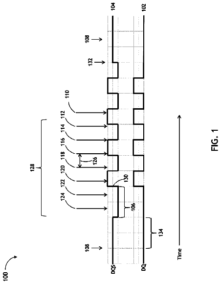
Sheet 1 of 23 from the published document. All sheets in the USPTO PDF
A multi-level dynamic random-access memory (MLDRAM) represents an original bit combination of more than one bit using a cell voltage stored in a single memory cell. The cell voltage is in one of a number of discrete analog voltage ranges each corresponding to a respective one of the possible values of the bit combination. In reading a selected memory cell, stored charge is conveyed via a local bitline to a preamplifier. The preamplifier amplifies the signal on the local bitline and drives a global bitline with an analog signal representative of the stored voltage. A digitizer converts the analog signal on the global bitline into a read bit combination. The read bit combination is then moved to a data cache over the global bitline. The data cache writes an analog voltage back to the memory cell to write a new value or restore data destroyed in reading the cell.
Dynamic random-access memory (DRAM) is a type of computer data storage. The term "random-access" alludes to the fact that data can be written to and read from designated addresses at random, as opposed to having to increment through a sequence of addresses to get to a designated location. DRAM stores digital data as representative voltages in storage capacitors. For example, a relatively high voltage or a relatively low voltage on a given capacitor can represent a logic one or a logic zero, respectively. The storage capacitors leak their stored charge, so the stored voltages quickly change with time. The information the voltages represent thus fades unless the stored voltages are periodically refreshed. That is, each memory cell is read and the voltage on it refreshed before the stored voltage has an opportunity to change so much that it no longer represents the originally stored data. E
1 of 23 drawing sheets so far from the published document, cropped to the drawing. Every sheet is in the USPTO PDF.
What the patent claimed, word for word. All of it is now free to use.
Dynamic random-access memory (DRAM) is a type of computer data storage. The term "random-access" alludes to the fact that data can be written to and read from designated addresses at random, as opposed to having to increment through a sequence of addresses to get to a designated location. DRAM stores digital data as representative voltages in storage capacitors. For example, a relatively high voltage or a relatively low voltage on a given capacitor can represent a logic one or a logic zero, respectively. The storage capacitors leak their stored charge, so the stored voltages quickly change with time. The information the voltages represent thus fades unless the stored voltages are periodically refreshed. That is, each memory cell is read and the voltage on it refreshed before the stored voltage has an opportunity to change so much that it no longer represents the originally stored data.
Each DRAM memory cell of the type described above stores a single logical bit, which can represent either a one or a zero. For example, a stored voltage in a range above a reference voltage may represent a logic one and below the reference voltage a logic zero. Storage density could be increased if more than one bit could be stored in a single memory cell. This is the concept behind multilevel DRAM (MLDRAM). In general, in MLDRAM, an n-bit digital value is represented by a single voltage that can be in one of 2.sup.n voltage ranges. Each voltage range corresponds to a respective one of the 2.sup.n possible states of the n-bit value. In conventional DRAM, one bit is stored in a single memory cell using 2.sup.1=2 voltage ranges. In an example of MLDRAM, two bits can be stored in a single memory cell if the MLDRAM can reliably identify the one of 2.sup.2=4 voltage ranges to which the voltage belongs. In theory, a two-bit MLDRAM could increase the storage density by a factor of about two.
The main disadvantage of MLDRAM is that the greater number of voltage ranges used to represent the additional data bit or bits reduces the extent of each voltage range and, hence, the difficulty of reliably identifying the voltage range to which the voltage stored in the memory cell belongs. Further, the memory cells of MLDRAM may require more frequent refreshing because the stored voltages can more quickly decay to the next-lower voltage range. Practical MLDRAM circuits will require improved methods and circuits for storing, sensing, and refreshing voltages representing multiple bits.
The subject matter disclosed is illustrated by way of example, and not by way of limitation, in the figures of the accompanying drawings and in which like reference numerals refer to similar elements and in which:
FIG. 1A depicts a multi-level dynamic random-access memory (MLDRAM) 100 in accordance with one embodiment.
FIG. 1B is a flowchart 140 depicting how a memory cell MC in MLDRAM 100 of FIG. 1A is read from and written to in accordance with one embodiment.
FIG. 2A depicts a multi-level dynamic random-access memory (MLDRAM) 200 in accordance with another embodiment.
FIG. 2B is a flowchart 250 depicting a page access operation used to read from, write to, or refresh a page of memory cells MC (e.g., all the memory cells MC of FIG. 2A associated with wordline WL0).
FIG. 3A depicts a memory cell MC coupled to a preamplifier Pre0 via a local bitline BL, all of FIG. 2A, in accordance with one embodiment.
FIG. 3B is a diagram 350 illustrating the relationship between cell voltage Vcell and global bitline voltage Vgbl in accordance with an embodiment in which the cell voltage Vcell varies between ground potential and supply voltage VDD.
FIG. 3C is a flowchart 360 outlining how preamplifier Pre0 of FIG. 3A is used to read an associated memory cell MC.
FIG. 4A is a schematic diagram detailing another embodiment of preamplifier Pre0 of FIG. 2A, associated memory cells MC, and global and local bitlines GBL0 and BL.
FIG. 4B is a diagram illustrating the relationship between memory-cell voltage Vcell, global bitline voltage Vgbl, and write voltage Vw.
FIG. 5 is a timing diagram depicting the operation of preamplifier Pre0 as depicted in FIG. 4, which operation is identical to that of the other preamplifiers.
FIG. 6 depicts an embodiment of a digitizer DG0 of FIG. 2A, which may be identical to digitizers DG[3:1].
FIG. 7A is a level diagram 700 depicting the operation of digitizer DG0 of FIG. 6.
FIG. 7B is a level diagram 750 similar to diagram 700 of FIG. 7A but showing how the reference and write voltages can be distributed non-linearly to improve overall error margins for an embodiment in which the memory cell capacitors are referenced to ground potential and can be charged to from ground to VDD.
FIG. 8A is a detailed embodiment of a digitizer DG0 of FIG. 2A, which is identical to digitizers DG[3:1] in this example.
FIG. 8B depicts an embodiment of latch 825 in sense amplifier 805 of FIG. 8A.
FIG. 9 is a timing diagram depicting the operation of digitizer DG0 of FIG. 8.
FIG. 10 illustrates how the data cache/write circuits DC/W0 and DC/W1 of FIG. 2A are connected to respective global bitlines GBL[1:0] and data-line pairs DQ[3:0] in accordance with one embodiment.
FIGS. 11A, 11B, 11C, and 11D detail the set of four blocks DCWL11, DCWL10, DCWL01, and DCWL00 that collectively form the data cache/write circuit DC/W0 connected to the highlighted global bitline GBL0 of FIG. 2A and FIG. 10 in accordance with one embodiment.
FIG. 12 is a timing diagram 1200 depicting the operation of data cache/write circuit DC/W0 of FIGS. 10 and 11A-D.
FIG. 13 illustrates how data cache/write circuits DC/W0 and DC/W1 of FIG. 2A are connected to respective global bitlines GBL[1:0] and data-line pairs DQ[3:0] in accordance with another embodiment.
FIG. 14 details an embodiment of data cache DC0 implemented as shown in FIG. 13.
FIG. 15 depicts the layout of a portion of a MLDRAM integrated circuit (IC) 1500 in accordance with one embodiment.
FIG. 16 is a flowchart 1600 outlining a test and calibration procedure for an MLDRAM IC in accordance with one embodiment.
FIG. 17A is a flowchart expanding upon block 1610 of FIG. 16, in which voltage Vbias to the preamplifiers is calibrated.
FIG. 17B is a diagram 1750 relating bias voltage Vbias to bit-error rate BER.
FIG. 18A is a flowchart illustrating pre-amplifier verification 1612 of FIG. 16 in accordance with one embodiment.
FIG. 18B is a diagram of the relationship between cell voltage Vcell, global bitline voltage Vgbl, and reference voltage Vrlm0 for an exemplary preamplifier with less than ideal gain.
FIG. 19A is a flowchart illustrating reference-voltage calibration 1625 of FIG. 16 in accordance with one embodiment.
FIG. 19B is a diagram 1955 illustrating the relationship between reference voltage Vrlm0 and bit error rate (BER).
FIG. 20 depicts a multi-level DRAM IC 2000 in accordance with one embodiment.
Dynamic random-access memory (DRAM) is a type of RAM that stores digital data as representative voltages across storage capacitors. For example, a relatively high or a relatively low voltage on a given storage capacitor can represent a logic one or a logic zero, respectively. The storage capacitors leak their stored charge, so the stored voltages quickly change with time. The information the voltages represent thus fades unless the stored voltages are periodically refreshed. That is, each storage cell is read and the voltage on it refreshed before the stored voltage has an opportunity to change so much that it no longer represents the originally stored data. In modern DRAM circuits, millions of capacitive memory cells must be refreshed at intervals measured in milliseconds. DRAM is therefore active even absent the reading or writing of data, and this essentially constant activity is why DRAM is referred to as "dynamic."
The need to dynamically refresh DRAM memory cells presents difficulties, but these difficulties are usually outweighed by the structural simplicity of the DRAM memory cell. Only a single access transistor is required for a DRAM memory cell, compared with a minimum of four transistors for other types of RAM. The relatively small and simple DRAM memory cell allows DRAM to reach very high storage densities at a cost that is low relative to alternative memory technologies. These advantages have lead to the widespread use of DRAM technologies in e.g. servers, workstations, personal computers, digital televisions, and set-top boxes.
FIG. 1A depicts a highly simplified example of a multi-level dynamic random-access memory (MLDRAM) 100 in accordance with one embodiment. MLDRAM 100 includes an array of memory cells MC, an exemplary one of which is shown at 102. Each of the memory cells stores a cell voltage Vcell representing two or more two binary digits, or bits, in a storage capacitor. The two or more bits represented by the cell voltage is referred to as a bit combination. In the examples described herein, each bit combination is composed of two bits. In other examples, each bit combination is composed of more than two bits. For bit combinations having n bits, 2.sup.n possible bit combinations exist.
In MLDRAM 100, each of the four possible bit combinations having two bits is represented by setting voltage Vcell to a voltage within a corresponding one of four voltage ranges. These voltage ranges are named to indicate the bit combinations they represent; namely, the relatively high voltage range Vc00 represents bit combination 00, a lower voltage range Vc01 represents bit combination 01, a still lower voltage range Vc10 represents bit combination 10, and the lowest voltage range Vc11 represents bit combination 11. Other relationships between voltage ranges and the bit combinations they represent are possible and may be used, and additional voltage ranges can be used to enable the voltage stored in each memory cell to represent bit combinations composed of additional bits. For example, eight voltage ranges can be used to enable the voltage stored in each memory cell to represent bit combinations composed of three bits.
An access transistor in each memory cell selectively couples a respective integrated or parasitic storage capacitor to one of two local bitlines BL[1:0]. The access transistors operate in response to wordline signals on corresponding wordlines WL[3:0]. Using a memory cell 102 as an example, asserting wordline signal WL0 on the corresponding signal line causes access transistor 104 to couple the storage capacitor 106 to local bitline BL0, and thus brings the local bitline voltage Vlbl to a voltage proportional to the cell voltage Vcell. Local bitline BL has a capacitance substantially greater than that of storage capacitor 106, so that the change in the voltage Vlbl on local bitline BL resulting from imposing cell voltage Vcell thereon is small. Moreover, the voltage ranges of local bitline voltage Vlbl that correspond to the above-described voltage ranges of cell voltage Vcell span a very small range of voltage and would therefore be difficult to distinguish from one another.
In MLDRAM 100, each local bitline BL[1:0] is connected to a respective preamplifier Pre[1:0], which amplifies the respective local bitline voltage to provide an analog global bitline voltage Vgbl on a global bitline GBL. The preamplifier compensates for the attenuation of cell voltage Vcell when the cell voltage is imposed on local bitline BL so that the gamut of global bitline voltage Vgbl is nominally equal to that of cell voltage Vcell, and global bitline voltage Vgbl has voltage ranges similar to those of cell voltage Vcell.
The global bitline connects preamplifiers Pre[1:0] to a digitizer DG, a data cache DC, and a write circuit W. Digitizer DG converts global bitline voltage Vgbl on global bitline GBL to a two-bit bit combination having a most-significant bit (MSB) and a least-significant bit (LSB). Since the gamut of global bitline voltage Vgbl on global bitline GBL is nominally equal to that of cell voltage Vcell, digitizer DG can reliably determine the voltage range to which global bitline voltage Vgbl belongs, and can therefore reliably generate the appropriate bit combination. Data cache DC stores the MSB and LSB from digitizer DG when reading from a memory cell, or accepts a new MSB and a new LSB from data lines DQ1 and DQ0 when such new bit combination is to be written to a memory cell. Write circuit W selects a write voltage Vw of a level corresponding to the MSB and LSB stored in data cache DC, and outputs the write voltage for writing to a selected memory cell during refresh or write operation.
FIG. 1B is a flowchart 140 depicting how exemplary memory cell 102 in MLDRAM 100 of FIG. 1A is read from, refreshed, and written to in accordance with one embodiment. With reference to FIG. 1A, this example assumes the bit combination of interest is (when a read operation is performed), or will be (when a write operation is performed), represented by a voltage stored within memory cell 102 associated with wordline WL0 and preamplifier Pre0.
To begin, wordline WL0 is asserted to open memory cell 102 (150), thus sharing the charge stored in the memory cell with local bitline BL0. The cell voltage Vcell due to the stored charge represents a bit combination composed of more than one bit, so the local bitline voltage Vlbl that results from the charge sharing likewise represents such bit combination. Preamplifier Pre0 amplifies local bitline voltage Vlbl and imposes the resulting analog voltage onto global bitline GBL
as global bitline voltage Vgbl. Global bitline voltage Vgbl is proportional to and is inverted with respect to local bitline voltage Vlbl, and consequently to cell voltage Vcell, and thus preserves the information read from memory cell 102. The voltage ranges for voltage Vgbl are named to indicate the respective bit combinations they represent, with the relatively high voltage range Vgbl11 representing bit combination 11, a lower voltage range Vgbl10 representing bit combination 10, a still lower range Vgbl01 representing bit combination 01, and the lowest voltage range Vgbl00 representing bit combination 00. As with the cell and bitline voltages, other relationships between voltage ranges and represented bit combinations are possible and may be used.
Digitizer DG compares the global bitline voltage Vgbl received from the global bitline with three reference voltages Vrlm0, Vrm, and Vrlm1 to identify which voltage range the global bitline voltage Vgbl falls within, and thus to determine the bit combination, composed of an MSB and an LSB, represented by global bitline voltage Vgbl (154). For example, should global bitline voltage Vgbl fall within voltage range Vgbl10, then digitizer DG outputs a bit combination composed of an MSB=1 and an LSB=0.
Having thus determined the bit combination represented by the cell voltage stored in memory cell 102, digitizer DG serially imposes the MSB and LSB of the bit combination on global bitline GBL0. The MSB and LSB are successively latched by data cache DC (156). The MSB is latched before the LSB in this example, but the order can be reversed. Per decision 158, if the memory access is for a read operation, then data cache DC outputs the cached MSB and LSB received from digitizer DG via data lines DQ1 and DQ0, respectively (160). The MSB and LSB constitute a read bit combination that is identical to the original bit combination represented by cell voltage Vcell. Output operation 160 is skipped when a memory cell is accessed as part of a write or refresh transaction.
Reading the memory cell depletes the charge stored therein, and consequently destroys the data represented by the stored charge. The memory cell voltage Vcell is therefore refreshed using the MSB and LSB stored in data cache DC. Write circuit W is used for this purpose.
When refreshing or writing to memory cell 102, data cache DC presents the MSB and LSB to write circuit W, which responds by imposing on global bitline GBL the one of four write voltages Vw00, Vw01, Vw10, and Vw11 corresponding to the MSB and LSB (162). These write voltages, as their names imply, respectively represent bits 00, 01, 10, and 11 when stored in a memory cell. Preamplifier Pre0 associated with open memory cell 102 includes a pass gate (not shown) that conveys the write voltage from global bitline GBL to local bitline BL0 for storage in the open memory cell MC 102 (164). Finally, wordline signal WL0 is deasserted, or the wordline closed, to deactivate access transistor 104 and thus retain the write voltage in the now closed memory cell 102. Operations to write a voltage representing new data in memory cell 102 are performed in the manner disclosed above for the refresh operation except that the new data is conveyed to data cache DC via data lines DQ1 and DQ0 before the write operation begins at 162. The remaining memory cells MC are read from, refreshed and written to using operations similar to those just described.
FIG. 2A depicts an example of a multi-level dynamic random-access memory (MLDRAM) 200 in accordance with another embodiment. MLDRAM 200 includes an array of memory cells MC, an exemplary one of which is shown at 102. Each of the memory cells, in the example shown, stores a cell voltage Vcell that represents two bits of information. Cell voltage Vcell is set to a voltage within one of four voltage ranges, each of which represents a respective bit combination composed of two bits. These voltage ranges are named to indicate the respective bit combinations they represent; namely, the relatively high voltage range Vc00 represents bit combination 00, a lower voltage range V01 represents bit combination 01, a still lower voltage range Vc10 represents bit combination 10, and the lowest voltage range Vc11 represents bit combination 11. Other relationships between voltage ranges and bit combinations may be used, and cell voltage Vcell can be divided into more or fewer ranges to represent more or fewer bits.
MLDRAM 200 includes a number of duplicate structures. These include data cache/write circuits DC/W[3:0], digitizers DG[3:0], preamplifiers Pre[3:0], data amplifiers 220, 222, and data buffers 225, 227. MLDRAM 200 additionally includes row and column decoders 230 and 235, and control logic 240 to manage the flow of data to and from memory cells MC. The following discussion details the operation of MLDRAM 200 using signal paths and circuit elements highlighted using relatively bold lines. The remaining similar structures behave similarly, so a discussion of those is omitted for brevity. A practical implementation of an MLDRAM will support many more rows and columns of memory cells than are depicted in FIG. 2A.
MLDRAM 200 stores information in arrays of memory cells MC arranged in rows and columns. Contrary to the normal meanings of "row" and "column" in the DRAM art, the columns are arranged from top to bottom and the rows are arranged from left to right in FIG. 2A. Each row of memory cells, commonly called a "page," is uniquely addressable using a row address Radd. Row decoder 230 decodes a specified row address Radd to assert one of N wordlines WL[N-1:0], which opens each memory cell MC of the page. To "open" a memory cell is to present its contents on a respective local bitline BL, so opening a page of memory cells presents the stored voltages of a page of memory cells on respective local bitlines BL. Each access operation activates an entire page (row) of memory cells, so data transfers that read or write to MLDRAM 200 are collectively referred to as "page-access operations." Refresh operations are also accomplished on a per-page basis, and can likewise be considered a type of page-access operation. In this example, a wordline signal WL0 on the like-identified wordline is asserted to open eight memory cells MC.
Columns or groups of columns are uniquely addressable using a column address Cadd. Column decoder 235 decodes a specified column address Cadd to assert one of column-select lines CSL[1:0]. In this embodiment, column decoder 235 can activate respective data cache/write circuits DC/W[0:3] associated with four memory cells MC of an open page by asserting one of column select lines CSL0 or CSL1. Each memory cell stores a cell voltage Vcell that represents a bit combination composed of two bits, so activating the data cache/write circuits associated with four memory cells allows cell voltages representing eight bits to be read from or written to the memory cells. Assuming column select line CSL1 is asserted, the uppermost four memory cells associated with wordline WL0 are enabled for read or write access.
The array of memory cells MC is divided into sub-arrays disposed between vertical stripes of preamplifiers. The wordlines WL extend over the sub-arrays and between the stripes of preamplifiers from a perspective normal to the device substrate, and to the illustration of FIG. 2A. Preamplifiers Pre[3:0] are laid out such that alternate local bitlines BL connect to preamplifiers in alternate stripes. This arrangement is used to relax the pitch of the preamplifiers.
Preamplifiers Pre[3:0] are coupled to respective digitizers DG[3:0] via global bitlines GBL[3:0]. Though shown outside of the memory arrays from a perspective normal to the device substrate in FIG. 2A, the global bitlines can extend over the memory cells in other embodiments. This routing can be accomplished using relatively long vias to interconnect the global bitlines to the underlying transistors, which in turn necessitates relatively large contact areas for the vias. Alternating the preamplifiers, as shown, to relax the pitch of the digitizers and preamplifiers makes it easier to accommodate these larger contact areas. Multiple local bitlines BL can be switchably connected to a shared preamplifier to further relax the pitch of the digitizers.
FIG. 2B is a flowchart 250 depicting a page access operation used to read from, write to, or refresh a page of memory cells MC (e.g., all the memory cells MC of FIG. 2A associated with wordline WL0). For simplicity, the access operation of flowchart 250 is described with reference to exemplary memory cell 102, the uppermost memory cell associated with wordline WL0 of FIG. 2A. The highlighted memory cell 102 is assumed to be accessed either for refresh purposes, to read from the memory cell, or to write new data to the memory cell.
Before the access starts, the local and global bitlines BL and GBL[3:0] are pre-charged to a known voltage level, such as ground potential (255). The pre-charged bitlines are then allowed to float at their respective pre-charge levels in preparation for receiving charge from memory cell 102 (257). Wordline signal WL0 is then asserted to open the corresponding page of memory cells, and consequently to convey their contents to respective preamplifiers Pre[3:0] via respective local bitlines BL (259). Memory cell 102 is coupled to preamplifier Pre0 via an associated local bitline BL: the flow of charge from the memory cell 102 of FIG. 2A is illustrated using a dashed arrow 260. All of the other open memory cells behave identically, so a detailed discussion of the other open memory cells is omitted for brevity.
Still following dashed arrow 260 of FIG. 2A, preamplifier Pre0 amplifies the voltage change on the local bitline BL that results from charge sharing between the open memory cell 102 and the capacitance of the local bitline, and imposes the resulting amplified analog signal on global bitline GBL0 as global bitline voltage Vgbl (261). In the depicted embodiment, preamplifier Pre0 inverts the sense of cell voltage Vcell in producing global bitline voltage Vgbl. The voltage ranges voltage Vgbl takes to represent each bit combination are therefore inverted compared with the corresponding voltage ranges of cell voltage Vcell. Relatively high memory-cell voltages Vcell thus produce relatively low global bitline voltages Vgbl, and vice versa. For example, preamplifier Pre0 amplifies a memory cell voltage Vcell within the lowest voltage range Vc11 to produce a global bitline voltage Vgbl within the highest voltage range Vglb11. The behaviors of embodiments of preamplifier Pre0 are detailed below.
Global bitline voltage Vgbl on global bitline GBL0, whatever its level, is presented to digitizer DG0. Digitizer DG0 latches a bit combination of two bits corresponding to global bitline voltage Vgbl (263). The latched bits are identical to the bit combination originally represented by cell voltage Vcell. Digitizer DG0 does this by comparing the global bitline voltage Vgbl with three reference voltages Vref to find the most-significant bit (MSB) and least-significant bit (LSB) of the bit combinations. From lowest to highest, the three reference voltages are Vrlm0, Vrm, and Vrlm1. In brief, digitizer DG0 interprets global bitline voltages Vgbl above the middle reference voltage Vrm as representing an MSB of one, and global bitline voltages below reference voltage Vrm as representing an MSB of zero. With the MSB resolved, digitizer DG0 determines the LSB by comparing global bitline voltage Vgbl with the lowest reference voltage Vrlm0 if the MSB is zero or the highest reference voltage Vrlm1 if the MSB is one. Embodiments of digitizer DG0--and identical digitizers DG[3:1]--are described below.
Digitizer DG0 imposes the MSB onto global bitline GBL0 (265), as a relatively high or a relatively low voltage representing a one and a zero, respectively. The data cache portion of data cache/write circuit DC/W0 then latches the MSB. The information flow is indicated by arrow 266 in FIG. 2A (267). Digitizer DG0 and data cache/write circuit DC/W0 repeat these operations for the LSB (271, 273) so that both the MSB and LSB are cached in the data cache/write circuit. In this example the global bitline GBL0 conveys both the analog global bitline voltages Vgbl to digitizer DG0 and the digital MSB and LSB from digitizer DG0. This dual use reduces the number of conductors needed to implement MLDRAM 200, and thus saves valuable die area. In other embodiments a separate line from digitizer DG0 to data cache/write circuit DC/W0 might also be used to convey the MSB and LSB.
At this point in the process, preamplifier Pre0, digitizer DG0, and data cache/write circuit DC/W0 have cached the bit combination represented by the cell voltage read from memory cell 102 coupled to the open wordline WL0. The preamplifiers, digitizers, and data cache/write circuits associated with the other open memory cells have likewise cached the respective bit combinations represented by the voltages stored in those memory cells. The data cache/write circuits DC/W[3:0] associated with column select signals CSL1 and CSL0 thus cache the bit combinations represented by the voltages read from all the open memory cells MC coupled to wordline WL0. In other words, the data caches collectively contain an entire page of data.
This example assumes wordline WL0 has been opened as part of a read access to the uppermost four memory cells, namely, memory cell 102 and the three neighboring memory cells similarly highlighted along wordline WL0. The voltages stored in each of these four memory cells has been sensed and the corresponding MSB and LSB have been cached in a respective one of the data cache/write circuits DC/W[3:0] connected to column select line CSL1. To access this information, column select line CSL1 is asserted to couple the outputs of the upper set of four data cache/write circuits DC/W[3:0] to pairs of data output lines. For example, the highlighted cache/write circuit DC/W0 contains the bit combination obtained by reading the memory cell 102, and a digital signal representative of each of the two bits constituting the bit combination is applied to data lines DQ0 and DQ1, respectively, and from there to data amplifier 220 and buffer 225. The remaining cache/write circuits DC/W[3:1] that receive the asserted column select signal on line CSL1 likewise deliver their bit combinations on the six remaining data lines DQ[7:2]. The eight bits obtained by reading from the four highlighted memory cells, i.e., memory cell 102 and its three closest neighbors on wordline WL0, are thus made available at the outputs of buffers 225 and 227.
In read and refresh operations, the entire page stored in the data cache/write circuits DC/W[3:0] is written back to the open page of memory cells MC. Write operations are similar, except that write data received via external data lines DQ[7:0] is cached in a selected column of data cache/write circuits DC/W[0:3] before the page is written to the memory cells. In short, read and refresh operations simply retain the contents of data cache/write circuits DC/W[3:0], and write operations modify the contents of cache/write circuits DC/W[3:0] with the new data to be stored. These two possibilities are shown in FIG. 2B as 275.
Data cache and write circuit DC/W0 writes the bit combination cached therein to memory cell 102 as one of four write voltages Vw, each representing a respective one of the four possible bit combinations. To write to memory cell 102 in FIG. 2A, data cache/write circuit DC/W0 selects one of the four write voltages corresponding to the combination of MSB and LSB cached therein, and imposes the selected write voltage Vw on global data bitline GBL0 (277). The write voltage Vw is then written to the memory cell via global bitline GBL0, a pass gate in preamplifier Pre0 (FIG. 4A), and local bitline BL (279). With the appropriate write voltage written to the selected memory cell 102, row decoder 230 closes wordline WL0 (281), and all the global and local bitlines are once again pre-charged in anticipation of the next page access (283).
FIG. 3A depicts an example of memory cell MC coupled to an example of preamplifier Pre0 via a local bitline BL, all of FIG. 2A, in accordance with one embodiment. When wordline WL0 is asserted to open memory cell MC, the local bitline BL takes a voltage Vbl representative of the stored cell voltage Vcell, and thus of the bit combination represented by cell voltage Vcell. Preamplifier Pre0 amplifies bitline voltage Vbl to generate global bitline voltage Vgbl that likewise takes a value representative of the stored bit combination. The gamut of global bitline voltage Vgbl is divided into four voltage ranges Vgbl00, Vgbl01, Vgbl 10, and Vgbl 11, each of which represents the respective bit combination included in their respective labels (e.g., voltage range Vgbl00 represents bit combination 00). A digitizer, such as digitizer DG of FIG. 1A, determines the bit combination represented by global bitline voltage Vgbl, and, hence by the stored cell voltage Vcell.
FIG. 3B is a diagram 350 illustrating the relationship between cell voltage Vcell and global bitline voltage Vgbl for an example in which the gamuts of both the cell voltage Vcell and the global bitline voltage Vgbl are between ground potential and supply voltage VDD. Preamplifier Pre0 (FIG. 3A) is inverting, so the voltage ranges of cell voltage Vcell are inverted relative to those of global bitline voltage Vgbl. The voltage gamut between ground and VDD is divided into four voltage ranges, each of which represents a different bit combination. In the memory cells, the lowest voltage range Vc11, from about zero volts to about 1/6VDD, represents bit combination 11, and the highest range Vc00, from about VDD to VDD, represents bit combination 00. The high and low voltage ranges are each 1/6VDD, whereas the middle two voltage ranges Vc01 and Vc10 are twice as large at 1/3VDD. The reasons for the non-uniform voltage ranges are explained below in connection with FIGS. 4A and 4B.
Returning to FIG. 3A, memory cell MC conventionally includes a transistor 300 coupled to a storage capacitor 305 and controlled by wordline WL0. Capacitor 305, an integrated component or a parasitic capacitance, exhibits a memory-cell capacitance Cmc and is referenced to half the supply voltage VDD in this embodiment. When wordline signal WL0 is asserted, transistor 300 allows charge stored in capacitor 305 to charge the bitline capacitance Cbl of local bitline BL, and to consequently change local bitline voltage Vbl. The memory cell capacitance Cmc is much smaller than bitline capacitance Cbl, so the charge sharing between the two produces a relatively small voltage change on local bitline BL. Though smaller, the voltage change on bitline BL is proportional to the originally stored cell voltage Vcell, and this proportionality preserves the information originally represented by cell voltage Vcell. Preamplifier Pre0 amplifies the voltage Vbl on local bitline BL and imposes the resulting amplified analog voltage on signal on global bitline GBL0 as global bitline Vgbl.
Preamplifier Pre0 includes an input transistor 310 with current-handling terminals connected to respective ones of a charge reservoir capacitor 312 and a sense node 314. A sense node capacitor 316 is connected to sense node 314. In some implementations, the gate capacitance of transistor 315 connected to sense node 314 and other parasitic capacitances provide sense node capacitor Csn. Charge reservoir capacitor 312 and sense node capacitor 316 are also connected to a supply or reference-voltage node, such as VSS or VBB. VSS and VBB are, respectively, the electrical bias voltages applied respectively to the sources and p-wells of NMOS transistors. Input transistor 310 additionally has a body node connected to bias voltage node VBB. In setting up the bias on the body node of transistor 310, a negative value for voltage VBB may be selected to raise the effective threshold voltage of transistor 310, and thus reduce the sub-threshold leakage current of the device. The other NMOS transistors constituting preamplifier Pre0 can have the same or a different body bias.
Preamplifier Pre[3:0] additionally includes transistors 315, 320, 325, and 330. Transistors 315, 320, 325, and 330 constitute a buffer amplifier that, when activated by control signal RD is capable of imposing sense node voltage Vsn on global bit line GBL0 while imposing only a small capacitive load on sense node 314. The gate of transistor 315 is connected to sense node 314, and the gate of transistor 320 is connected to the source of transistor 315. The drains of transistors 315 and 320 are connected to supply VDD. Transistors 325 and 330 are connected in series between the sources of transistors 315 and 320, respectively, and global bitline GBL0. The gates of transistors 330 and 325 are connected to receive control signal RD that activates the transistors. With transistor 330 active in response to control signal RD, transistors 315 and 320 can be regarded as cascaded source followers. Transistor 315 is made small to reduce its gate capacitance, which contributes to the capacitance Csn of sense node capacitor 316. Making sense node capacitor (and hence transistor 315) small allows transistor 310 and charge reservoir capacitor 312 also to be relatively small. Transistor 320 is typically larger in area than transistor 315 and can therefore charge the capacitance of global bitline GBL0 much more quickly than transistor 315 could on its own.
FIG. 3C is a flowchart 360 outlining how preamplifier Pre0 of FIG. 3A is used to amplify bitline voltage Vbl when memory cell MC is being read. Referring additionally to FIG. 3A, memory cell 102 is read, capacitors 312 and 316 are precharged low and high, respectively (365). In this example, capacitor 312 is precharged to a near-ground bias voltage Vbias (FIG. 4), and capacitor 316 is precharged to one transistor threshold Vth above supply voltage VDD (i.e., to VPP=VDD+Vth).) Bitline capacitance Cbl is likewise precharged, e.g., to ground. The circuit elements used in precharging, omitted here for ease of illustration, are detailed below in connection with FIG. 4A. The precharge voltages on the source, drain, and gate of transistor 310 and the bias voltage VBB to the body terminal of transistor 310 are selected so that transistor 310 is on the verge of turning on.
Next, at 370, wordline WL0 is asserted to read cell voltage Vcell. Storage capacitor 305 shares charge with the parasitic capacitance Cbl of bitline BL until bitline voltage Vbl and the memory cell voltage Vcell reach equilibrium. The capacitance Cmc of storage capacitor 305 is considerably less than that of bitline capacitance Cbl, so the charge sharing between the two capacitances produces a change in bitline voltage Vbl that is small compared with the change in cell voltage Vcell. In an embodiment in which capacitance Cbl is ten times capacitance Cmc, cell voltage Vcell ranges from about zero to about 0.9 volts, and bitline capacitance Cbl is pre-charged to ground, for example, the bitline voltage after charge sharing ranges from about zero to about 0.09 volts.
Charge reservoir capacitor 312 can be fabricated of the same materials and have the same construction as storage capacitor 305 in memory cell 102. In this case, charge reservoir capacitor 312 can be referenced to half supply voltage VDD/2 as in the case of the cell capacitor Cmc as shown in FIG. 3A instead of VSS or VBB. The precharge voltages on the gate and source of transistor 310 (i.e., the precharge voltages on local bitline and charge reservoir capacitor 312) differ by the threshold voltage Vth of transistor 310, leaving transistor 310 on the verge of turning on. The increase in bitline voltage Vbl due to charge sharing will therefore cause transistor 310 to turn on, which allows charge to pass from sense-node capacitor 316 to charge reservoir capacitor 312. The charge transfer will continue until the voltage on charge reservoir capacitor 312 rises to within the threshold voltage Vth of transistor 310 of the increased bitline voltage Vbl. In this way, the change of bitline voltage Vbl that occurs as a result of reading memory cell MC is replicated as a change in the voltage on charge reservoir capacitor 312. For example, opening memory cell 102 with a memory cell voltage Vcell of 0.9 volts causes bitline voltage Vbl to rise from a precharge voltage of zero to 0.09 volts. The gate of transistor 310 would thus rise 0.09 volts above the threshold voltage required to turn transistor 310 on. Charge thus transfers through transistor 310 from sense node capacitor 316 to charge reservoir capacitor 312 until the voltage across capacitor 312 increases by 0.09 volts. When this occurs, transistor 310 turns off.
The description continues in the full USPTO document.
About 6,302 words. The USPTO PDF has it with every drawing.
Fees are due 3.5, 7.5 and 11.5 years after grant. This patent expired on July 8, 2026, so the fee marked "not paid" was the one that went unpaid.
Multilevel DRAM
Filed Dec 2010 · published Dec 2012Multilevel DRAM
Filed Dec 2010 · granted Jul 2014Earlier publications, parents and continuations. None of them can still be enforced, or this patent would not be listed.
Prior art cited by the examiner or applicant. Useful when you check your own idea for novelty.
Everything on this page comes from the documents linked above.