 Lapsed, fee not paid5 drawings
Hardware & Electronics · US 8,766,872 B2
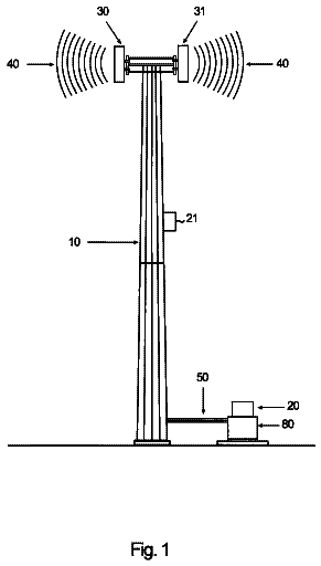
Autonomous wireless antenna sensor system
Systems and methods are enclosed for processing antenna position information.
US 8,767,189 B2 · Assignee: Hamamatsu Photonics K.K. · Inventors: Mase; Mitsuhito et al.
Sheet 1 of 37 from the published document. All sheets in the USPTO PDF
A pair of first gate electrodes IGR, IGL are provided on a semiconductor substrate 100 so that potentials .phi..sub.TX1, .phi..sub.TX2 between a light-sensitive area SA and a pair of first accumulation regions AR, AL alternately ramp. A pair of second gate electrodes IGR, IGL are provided on the semiconductor substrate 100 so as to control the height of first potential barriers .phi..sub.BG each interposed between the first accumulation region AR, AL and a second accumulation region FDR, FDL, and increase the height of the first potential barrier .phi..sub.BG to carriers as a higher output of a background light is detected by a photodetector.
The following Patent Document 1 discloses a TOF (Time Of Flight) type distance image measurement device. This distance image measurement device repeatedly emits a probe light having a predetermined pulse width toward a subject and measures a period of time from an emission time to a return time of the probe light, that is, a time of flight of the probe light to thereby measure a three-dimensional distance image up to the subject. In this device, a phase difference between pulses at an emission and pulses at a return of a probe light is measured as a time of flight. Time of flight measuring methods include one that determines a ratio of the amount of charge accumulated in a plurality of accumulation regions formed in each pixel. In Patent Document 2, the accumulation timings in the charge accumulation regions are differentiated. The ratio of the amount of charge generated in each accumula
1 of 37 drawing sheets so far from the published document, cropped to the drawing. Every sheet is in the USPTO PDF.
What the patent claimed, word for word. All of it is now free to use.
The present invention relates to a solid state imaging device and a distance image measurement device.
The following Patent Document 1 discloses a TOF (Time Of Flight) type distance image measurement device. This distance image measurement device repeatedly emits a probe light having a predetermined pulse width toward a subject and measures a period of time from an emission time to a return time of the probe light, that is, a time of flight of the probe light to thereby measure a three-dimensional distance image up to the subject. In this device, a phase difference between pulses at an emission and pulses at a return of a probe light is measured as a time of flight.
Time of flight measuring methods include one that determines a ratio of the amount of charge accumulated in a plurality of accumulation regions formed in each pixel. In Patent Document 2, the accumulation timings in the charge accumulation regions are differentiated. The ratio of the amount of charge generated in each accumulation region due to incidence of one reflected pulse light is proportional to the time of flight, by eliminating a background light component. For example, an accumulation timing in one accumulation region is set in accordance with the period of time from a rising time to a falling time of probe light pulses, and an accumulation timing in the other accumulation region is set in accordance with the period of time from a falling time and a rising time. In this case, with zero time of flight, if the amount of accumulated charge in one accumulation region is 100%, the amount of accumulated charge in the other accumulation region is 0%, so that the distance up to a target is zero. The longer the time of flight, the more the ratio of the amount of accumulated charge in the other accumulation region increases, and thus the distance up to a target is determined according to the ratio of the charge amount. Patent Document 1: U.S. Pat. No. 6,373,557 specification Patent Document 2: International Publication No. WO 2006/010284 pamphlet
Problem to be Solved by the Invention
However, in the distance image measurement device described in Patent Document 2, four potential depths within individual pixels are simultaneously controlled, and at a point in time where carriers have flooded from all potential wells, the ratio of the charge amount of flooded carriers is calculated, so that there is a problem of complicating the device.
The present invention has been made in view of such problems, and an object thereof is to provide a solid state imaging device and a distance image measurement device capable of a distance image measurement with a simple configuration.
Means for Solving the Problem
In order to solve the above-described problems, a solid state imaging device according to the present invention is a solid state imaging device including photo-detection means for detecting a background light, and an imaging region consisting of a plurality of pixels, in which each of the pixels includes a light-sensitive area provided in a semiconductor substrate, a pair of first accumulation regions provided in the semiconductor substrate, a pair of first gate electrodes provided on the semiconductor substrate so that potentials between the light-sensitive area and a pair of the first accumulation regions alternately ramp, a pair of second accumulation regions provided in the semiconductor substrate, and a pair of second gate electrodes that are provided on the semiconductor substrate so as to control the height of first potential barriers each interposed between the first accumulation region and the second accumulation region, and increase the height of the first potential barrier to carriers as a higher output of a background light is detected by the photo-detection means.
In addition, the height of the potential barrier is, when the carriers are electrons, increased relative to a potential where electrons exist, by decreasing the potential, and reduced by increasing the potential. Alternatively, when the carriers are holes, the height of the potential barrier is, relative to a potential where holes exist, increased by increasing the potential, and is reduced by decreasing the potential.
When a pulsed probe light for distance detection is irradiated onto a target and voltages where the foregoing potential ramp alternately occurs are applied to the first gate electrodes, the charge amount of carriers to be accumulated in one first accumulation region is reduced, and the charge amount of carriers to be accumulated in the other first accumulation region is increased, in proportion to a delay at the incidence of a reflected light of a probe light. More specifically, the ratio of these charge amounts of accumulated carriers depends on the delay time, that is, time of flight (TOF). As a matter of course, when the number of first accumulation regions is three or more, the ratio of carriers flowing in each first accumulation regions from the light-sensitive area depends on the phases of application voltages to potential ramping electrodes interposed between these, and the carrier accumulation changes in amount by a shift in phase. In addition, the charge amount of carriers accumulated in the first accumulation region contains a carrier component generated in response to a background light component, so that the ratio of carriers after elimination of carriers corresponding to the background light component indicates the distance. Moreover, the probe light is not limited to be pulsed but may also be sinusoidal. In that case, the voltages to be applied to the first gate electrodes are also made sinusoidal.
Here, if output of a background light detected by the photo-detection means is high, the second gate electrode increases the height of the first potential barrier to carriers. The first potential barrier is interposed between the first accumulation region and the second accumulation region, the number of carriers flowing in the second accumulation region from the first accumulation region is reduced as the background light becomes higher. More specifically, appropriately controlling the voltage to be applied to the second gate electrode according to the size of a background light makes it possible to simply block carriers corresponding to the background light by the first potential barrier and allow only a reflected light component of a probe light from the target to flow in the second accumulation region. The height of the first potential barrier may be reduced
after performing this measurement (accumulation period of time of carriers into the first accumulation region) after detecting a background light, or may be reduced in advance
before performing this measurement (accumulation period of time of carriers into the first accumulation region) after detecting a background light.
Moreover, the solid state imaging device according to the present invention includes a pair of third accumulation regions provided in the semiconductor substrate, and a pair of third gate electrodes provided on the semiconductor substrate so as to control the height of second potential barriers each interposed between the second accumulation region and the third accumulation region, and in which by lowering the height of the second potential barrier to carriers, carriers accumulated in the second accumulation region are transferred to the third accumulation region, and then the height of the second potential barrier is increased, and with the carriers held in the third accumulation region, application potentials to the first, second, and third gate electrodes are controlled so that carriers are alternately accumulated in a pair of the first accumulation regions.
More specifically, when carriers of the last measurement have been accumulated in the second accumulation region, if the first gate electrode is driven in this measurement, the carriers will be mixed. However, in the present example, if the height of the second potential barrier is lowered to transfer the carriers to the third accumulation regions and then the height of the second potential barrier is increased to prevent carriers from flowing in from the second accumulation region to the third accumulation region, the first gate electrode can be driven at this stage to make carriers generated in this measurement flow in the second accumulation region from the light-sensitive area.
Moreover, preferably, the light-sensitive area serves also as the above-mentioned photo-detection means, and the solid state imaging device further includes control means that outputs an application potential to the second gate electrode according to an output of the light-sensitive area. More specifically, a background light is detected in the light-sensitive area, and if output of the detected background light is large, the application potential to the second gate electrode is controlled so that the height of the first potential barrier is increased, and if output is small, the application potential to the second gate electrode is controlled so that the height of the first potential barrier is reduced. This makes it unnecessary to provide photo-detection means separately, so that downsizing of the device is enabled.
Moreover, a distance image measurement device according to the present invention includes the foregoing solid state imaging device, a light source for emitting a pulse light being in synchronization with an application potential to a pair of the first gate electrodes to a target, and a calculating circuit for calculating a distance up to the target according to a charge amount of carriers output from a pair of the second accumulation regions.
In this distance image measurement device, the charge amount of carriers is according to the distance up to the target, so that it becomes possible to output a distance image of the target from the calculating circuit.
Effects of the Invention
The solid state imaging device according to the present invention can be applied to a distance image measurement with a background light component eliminated although the configuration of which is simple, and the distance image measurement device, despite being simple, is capable of measuring an accurate distance image.
FIG. 1 is a view for explaining an outline of a distance image measurement device.
FIG. 2 is a perspective view of a solid state imaging element 1.
FIG. 3 is a view showing a distance image that is generated from an image for distance acquisition projected onto an imaging region 1IP.
FIG. 4 is a view for explaining a measurement principle of a distance d up to an object H.
FIG. 5 is a timing chart of a drive pulse signal S.sub.P, a detection pulse signal S.sub.D, a right pulse signal S.sub.R, and a left pulse signal S.sub.L.
FIG. 6 are explanatory views for explaining an accumulation principle of carriers.
FIG. 7 is a block diagram for explaining a calculation of the distance d.
FIG. 8 is a plan view of a solid state imaging element 1.
FIG. 9 are views for explaining a detailed structure of each pixel P(m, n).
FIG. 10 are potential diagrams for explaining an accumulation and discharge operation of carriers.
FIG. 11 is a block diagram showing an internal configuration of a background light elimination circuit PCC.
FIG. 12 is a graph for explaining a calculation in a calculating circuit CC.
FIG. 13 is a circuit diagram within each pixel P(m, n).
FIG. 14 is a circuit diagram of a solid state imaging element 1 formed by arraying the pixels P(m, n) shown in FIG. 13.
FIG. 15 is a circuit diagram of a Sample holding circuit SHn shown in FIG. 8.
FIG. 16 is a timing chart of a solid state imaging device.
FIG. 17 is a plan view of an imaging region 1IP showing an arrangement example of pixels P and photodetectors PD.
FIG. 18 is a plan view of an imaging region 1IP showing an arrangement example of pixels P and photodetectors PD.
FIG. 19 is a plan view of an imaging region 1IP showing an arrangement example of pixels P and photodetectors PD.
FIG. 20 is a circuit diagram of a pixel P(m, n) and amplifiers.
FIG. 21 is a circuit diagram of a pixel P(m, n) and amplifiers.
FIG. 22 is a plan view of a solid state imaging element 1 having pixels with an electrode array modified.
FIG. 23 are a plan view (FIG. 23(A)) of the pixel P(m, n) shown in FIG. 22, a longitudinal sectional view (FIG. 23(B)) of the pixel P(m, n), and a potential diagram (FIG. 23(C)) in a semiconductor at no bias in the longitudinal sectional view.
FIG. 24 are potential diagrams for explaining an accumulation and discharge operation of carriers.
FIG. 25 is a time chart diagram showing a relationship between carrier accumulation and readout.
FIG. 26 is a circuit diagram of the pixel P(m, n) shown in FIG. 23.
FIG. 27 is a circuit diagram of a solid state imaging element 1 formed by arraying the pixels P(m, n) shown in FIG. 26.
FIG. 28 is a timing chart of a solid state imaging device with a charge buffer region.
FIG. 29 is a plan view of a solid state imaging element 1 having four gate electrodes for carrier distribution per one pixel.
FIG. 30 is a plan view of the pixel P(m, n) shown in FIG. 29.
FIG. 31 are a sectional view (FIG. 31(A)) taken along arrows 31A-31A in FIG. 30, a potential diagram (FIG. 31(B)) in a semiconductor at no bias in the sectional view of FIG. 31(A), a sectional view (FIG. 31(C)) taken along arrows 31C-31C in FIG. 30, and a potential diagram (FIG. 31(D)) in a semiconductor at no bias in the sectional view of FIG. 31(C).
FIG. 32 is a circuit diagram of the pixel P(m, n) shown in FIG. 30.
FIG. 33 is a circuit diagram of a solid state imaging element 1 formed by arraying the pixels P(m, n) shown in FIG. 32.
FIG. 34 is a circuit diagram of a Sample holding circuit SHn' shown in FIG. 29.
FIG. 35 is a timing chart of a solid state imaging device.
FIG. 36 is a block diagram showing a modification of a background light elimination circuit PCC.
FIG. 37 is a timing chart of a solid state imaging device when self-reference type background light detection is performed.
1 Solid state imaging element
1IP Imaging region
1V Vertical shift register
1H2 Horizontal shift register
2 Controlling circuit
3 Light source
DEX1, DEX2 Carrier discharge region
DEX3, DEX4 Carrier discharge region
EX1, EX2 Gate electrode
EX3, EX4 Gate electrode
PCC Background light elimination circuit
PD Photodetector
Hereinafter, a solid state imaging device and a distance image measurement device according to an embodiment will be described. Also, the same elements are denoted by the same reference numerals and signs, and overlapping description will be omitted.
FIG. 1 is a view for explaining an outline of a distance image measurement device.
This distance image measurement device is mounted on a vehicle VG, and measures an object H that is located in front of the vehicle.
The distance image measurement device includes a solid state imaging element 1, a controlling circuit 2 that controls drive of the solid state imaging element 1, a light source 3 that emits pulse light, a driving circuit 4 of the light source 3, and an output processing circuit 5 incorporating a calculating circuit for calculating a distance up to the object H from output of the solid state imaging element 1. The controlling circuit 2 inputs a right pulse signal S.sub.R and a left pulse signal S.sub.L to the solid state imaging element 1, and inputs a drive pulse signal S.sub.P for light projection to the driving circuit 4. The drive pulse signal S.sub.P is input also to the output processing circuit 5, and used when calculating a distance from the solid state imaging element 1.
In synchronization with the drive pulse signal S.sub.P output from the controlling circuit 2, a drive current is supplied from the driving circuit 4 to the light source 3. From the light source 3, a probe light having the same pulse width as that of the drive pulse signal S.sub.P is emitted. The probe light is irradiated onto the object H via a light-projecting lens L1. The probe light reflected on the surface of the object H is made incident into an imaging region of the solid state imaging element 1 via imaging lenses L2, L3. Accordingly, an image of the object H is to be formed in the imaging region of the solid state imaging element 1.
From the solid state imaging element 1, (original data of) a distance image of the object H is output, and these data are processed by the output processing circuit 5, and displayed on a display unit 6 of a car navigation system. Although, on the display unit 6, a distance image can be independently displayed, it is also possible to display this distance image superimposed with a brightness image. In addition, when the object H indicated by the distance image exists within a predetermined distance, a warning display to the effect that the object H exists can also be displayed superimposed with the brightness image.
FIG. 2 is a perspective view of the solid state imaging element 1.
The solid state imaging element 1 includes an imaging region 1IP consisting of a plurality of pixels P(1, 1), P(1, 2), . . . P(m, n), . . . P(M, N) arrayed two-dimensionally. m, n, M, N is a natural number. In addition, for clarification of description, a smaller number of pixels than that in actuality are shown in the figure. A vertical shift register 1V is arranged parallel to pixel columns of the imaging region 1IP, and a background light elimination circuit PCC and a horizontal shift register 1H2 are arranged parallel to pixel rows.
The vertical shift register 1V sequentially applies, to each pixel P(m, n), a vertical transfer signal to read out output of pixels P(m, n) arrayed in a column direction, sequentially along the column direction. In each pixel column, a pixel output transferred in one vertical direction is input to distance information readout circuits K1, K2, . . . Kn . . . K.sub.N. The pixel outputs input to the distance information readout circuits K1, K2, . . . Kn K.sub.N are sequentially read out as (original data of) a distance image along the row direction.
More specifically, in a distance image measurement mode, when outputs of the first row pixels P(1, 1), P(1, 2) . . . P(1, n) P(1, N) are input to the distance information readout circuits K1, K2, . . . Kn . . . K.sub.N, respectively, the distance information readout circuits K1, K2, . . . Kn . . . K.sub.N once hold original data of a distance image for each of the input pixel outputs, and the held original data are, in a horizontal order, sequentially read out to the outside via an output buffer amplifier 1I. This horizontal readout is performed by sequentially inputting, from the horizontal shift register 1H2, a signal to turn on an output switch of each distance information readout circuit K1, K2, . . . Kn . . . K.sub.N to the output switch along the horizontal direction.
Next, outputs of the second row pixels P(2, 1), P(2, 2) . . . P(2, n) . . . P(2, N) are input to the distance information readout circuits K1, K2, . . . Kn . . . K.sub.N, respectively, and thereafter, the same operation as above is performed. When the same operation as above is thereafter performed for the third, fourth . . . to M-th row, the outputs from all pixels in the imaging region 1IP are to be read out as distance information.
At the time of non-irradiation of a probe light, projected onto the imaging region 1IP is a brightness image that is formed as a result of outside light such as sunlight or a street light being reflected on the surface of the object H. At the time of irradiation of a probe light, projected onto the imaging region 1IP superimposed with such a brightness image (background light) is an image for acquiring a distance up to the object H, which is formed of a reflected light of the probe light. The image for distance acquisition is a set of original data to calculate a distance image.
The background light elimination circuit PCC, according to the size of output of a background light detected by a photodetector (photo-detection means), controls the height of a potential barrier that controls the amount of charge flooding from each pixel. More specifically, in each pixel, a potential barrier is provided at a previous stage of its readout section, and when the background light is large, by increasing the height of the potential barrier, a background light component is eliminated from an output from each pixel. The potential barrier is adjusted by controlling potential to be applied to a gate electrode formed on a semiconductor substrate.
FIG. 3 is a view showing a distance image that is generated from an image for distance acquisition projected onto the imaging region 1IP. A rectangular coordinate system consisting of an M-axis, an N-axis, and a D-axis is set. In the figure, lines connecting distances indicated by the respective pixel outputs in the imaging region 1IP are shown in a network form. This distance image is calculated in the output processing circuit 5. In the imaging region 1IP, M rows and N columns of pixels are arrayed, and a distance vertical to the imaging region 1IP is shown on the D-axis. The distance image of the object H is a set of information of the distances (denoted by d) on the D-axis.
FIG. 4 is a view for explaining a measurement principle of the distance d up to the object H.
The driving circuit 4 has a switch 4b interposed between a power supply 4a and the light source 3, and when a drive pulse signal S.sub.P for light projection is input to the switch 4b, a drive current being in synchronization with the drive pulse signal S.sub.P is supplied to the light source 3, and a probe light (pulse light) L.sub.P being in synchronization with the drive pulse signal S.sub.P is emitted from the light source 3. Although the light source 3 of the present example is to be formed of a light-emitting diode or laser diode excellent in steepness of rise and fall of a pulse light, as a matter of course, it is also possible to use another type of light source. In addition, preferably, the light source 3 is formed of an infrared light-emitting diode.
When a probe light is irradiated onto the surface of the object H located at the distance d, the probe light is reflected on this surface, and the reflected probe light is made incident into the solid state imaging element 1 as a pulse light L.sub.D. The pulse light to be made incident into the solid state imaging element 1 is provided as L.sub.D, while a detection pulse signal to be output from a pixel as a result of the pulse light being made incident is provided as S.sub.D. On the solid state imaging element 1, the foregoing distance information readout circuit K is provided, and the foregoing right pulse signal S.sub.R and left pulse signal S.sub.L are input to the distance information readout circuit K.
It is also possible for the distance information readout circuit K to output a background light, and the background light indicates a brightness image of the target. For example, when a charge of a background light component remaining in two potential wells is read out, this serves as a brightness image q(m, n). The brightness image q(m, n) output from each pixel P(m, n) is input to the image processing circuit 5b.
In response to incidence of the detection pulse signal S.sub.D, from the distance information readout circuit K, distance information d'(m, n) serving as original data of a distance image is read out corresponding to each pixel P(m, n). The distance information d'(m, n) is input to a calculating circuit 5a, and converted to a distance image d(m, n) by using the drive pulse signal S.sub.P. The distance information d'(m, n) is a value depending on the time of flight of a probe light up to the object H. The distance image d(m, n) is input to the image processing circuit 5b together with the brightness image q(m, n) according to necessity. In the image processing circuit 5b, the foregoing superimposition processing and the like can be performed.
FIG. 5 is a timing chart of the drive pulse signal S.sub.P, the detection pulse signal S.sub.D, the right pulse signal S.sub.R, and the left pulse signal S.sub.L. The drive pulse signal S.sub.P has a pulse width of T.sub.P.
The right pulse signal S.sub.R rises in synchronization with a rising time t.sub.1 of the drive pulse signal S.sub.P. The right pulse signal S.sub.R falls in synchronization with a falling time t.sub.3 of the drive pulse signal S.sub.P. More specifically, the right pulse signal S.sub.R is in phase with the drive pulse signal S.sub.P. The left pulse signal S.sub.L, which is in opposite phase with the right pulse signal S.sub.R, falls at the time t.sub.1, and rises at the time t.sub.3. The right pulse signal S.sub.R and the left pulse signal S.sub.L both have a pulse width of T.sub.P.
When the detection pulse light L.sub.D is made incident into each pixel, carriers are generated in each pixel. A time waveform of the charge amount of carriers generated due to incidence of the detection pulse light L.sub.D matches the detection pulse signal S.sub.D.
Carriers generated in the pixels flow in one first accumulation region when the right pulse signal S.sub.R is high level. Thus, in this pulse cycle, a charge amount Q1 of carriers to be effectively accumulated in one first accumulation region is proportional to an overlapping period of time t.sub.2 to t.sub.3 between the detection pulse signal S.sub.D and the right pulse signal S.sub.R. In other words, a value of a product of the detection pulse signal S.sub.D and the right pulse signal S.sub.R a crest value of which indicates a charge amount per time having been integrated for a period of time t.sub.2 to t.sub.3 equals the charge amount Q1 to be accumulated in one first accumulation region. Moreover, in a next pulse cycle, a value of the product of the detection pulse signal S.sub.D and the right pulse signal S.sub.R having been integrated for a period of time t.sub.6 to t.sub.7 equals the charge amount Q1 to be accumulated in one first accumulation region.
Carriers generated in the pixels flow in the other first accumulation region when the left pulse signal S.sub.L is high level. Thus, in this pulse cycle, a charge amount Q2 of carriers to be effectively accumulated in the other first accumulation region is proportional to an overlapping period of time t.sub.3 to t.sub.4 between the detection pulse signal S.sub.D and the right pulse signal S.sub.R. In other words, a value of a product of the detection pulse signal S.sub.D and the left pulse signal S.sub.L a crest value of which indicates a charge amount per time having been integrated for a period of time t.sub.3 to t.sub.4 equals the charge amount Q2 to be accumulated in the other first accumulation region. Moreover, in a next pulse cycle, a value of the product of the detection pulse signal S.sub.D and the left pulse signal S.sub.L having been integrated for a period of time t.sub.7 to t.sub.8 equals the charge amount Q2 to be accumulated in the other second accumulation region.
The ratio of the charge amount Q1 and the charge amount Q2 is proportional to the time of flight (TOF). More specifically, the relatively larger the latter charge amount Q2 is than the former charge amount Q1, the greater the distance d. As a matter of course, the ratio of not only the charge amount accumulated in one pulse cycle but an integrated value .SIGMA.Q1, .SIGMA.Q2 of the charge amount Q1, Q2 is also proportional to the time of flight (TOF). In addition, performing integration makes it possible to obtain an accurate distance because the charge amount becomes large.
Here, where it is provided that a probe light is emitted in darkness, the ratio of the charge amount Q1, Q2 indicates the distance, however, because a charge component corresponding to a background light is in fact contained in the detection pulse signal S.sub.D, it is necessary to eliminate the background light component.
FIG. 6 are explanatory views for explaining an accumulation principle of carriers.
FIG. 6(A) is a sectional view of one pixel P(m, n).
The pixel P(m, n) includes a p-type (first conductivity type) semiconductor substrate 100 and an insulating layer 101 formed on the semiconductor substrate 100. On the insulating layer 101, a light-shielding film SM is provided. The light-shielding film SM includes light entrance openings OP on a pixel-by.-pixel basis On the insulating layer 101 directly below the opening OP, a pixel electrode PG is arranged. A surface area within the semiconductor substrate 100 directly below the pixel electrode PG of the semiconductor substrate 100 is provided as a light-sensitive area SA. At both sides of the pixel electrode PG, a pair of first gate electrodes TX1 and TX2 are arranged on the insulating layer 101. On the outside of the first gate electrodes TX1, TX2, a pair of first accumulation regions AR and AL provided in the semiconductor substrate 100 are located. Further, on the outside of the first accumulation regions AR, AL, a pair of second accumulation regions FDR and FDL provided in the semiconductor substrate 100 are located. The second accumulation regions FDR, FDL are floating diffusion regions. Above a region between the first accumulation regions AR, AL and the second accumulation regions FDR, FDL, second gate electrodes IGR, IGL are respectively located on the insulating layer 101.
The first accumulation region AR, AL and the second accumulation region FDR, FDL are each formed of an n-type semiconductor region. A positively ionized donor exists in an n-type semiconductor, and a negatively ionized acceptor exists in a p-type semiconductor. The potential in a semiconductor is higher in the n-type than in the p-type. In other words, because the potential in an energy band diagram is shown heading downward as the positive direction of potential, the potential in an n-type semiconductor is deeper (higher) than that of a p-type in the energy band diagram, and the energy level is lower. Moreover, when a positive potential is applied to each electrode, the potential of a semiconductor region directly below the electrode is deepened (increased in the positive direction). When the positive potential to be applied to each electrode is reduced in size, the potential of a semiconductor region directly below the electrode is made shallow (reduced in the positive direction).
FIG. 6(B) is a potential diagram when the right pulse signal S.sub.R to be applied to the right first gate electrode TX1 is high level. The left pulse signal S.sub.L to be applied to the left first gate electrode TX2 is low level. In addition, description will be given of the potential diagram assuming downward as positive, and a potential .phi. to be applied to each electrode and a potential .phi. of the semiconductor region directly below each electrode are denoted by the same sign.
A slight positive potential .phi..sub.PG is applied to the pixel electrode PG, and a positive potential .phi..sub.TX1 greater than .phi..sub.PG is applied to the right first gate electrode TX1. Accordingly, carriers (electrons) generated by the incidence of light into the light-sensitive area SA are induced by a potential gradient formed by .phi..sub.PG and .phi..sub.TX1, and flow in a position of a potential .phi..sub.AR of the first accumulation region AR existing in a deep position.
Next to the right first accumulation region AR is one adjacent second accumulation region FDR. A potential difference between a potential .phi..sub.AR of the first accumulation region AR and a potential .phi..sub.IGR of the semiconductor region directly below the second gate electrode IGR is provided as .phi..sub.BG. When this right first potential barrier .phi..sub.BG is large, the charge amount of carriers flowing in the second accumulation region FDR from the right first accumulation region AR is small, and when it is small, the charge amount of carriers flowing in the second accumulation region FDR from the first accumulation region AR is large.
From the background light elimination circuit PCC, a potential control voltage (.phi..sub.IGR, .phi..sub.IGL) corresponding to the size of a background light is output. This potential control voltage is applied to the pair of second gate electrodes IGR and IGL. In addition, when the potential of the semiconductor substrate 100 is provided at ground level, an application voltage and an application potential to each electrode match. In the present example, the potential of the semiconductor substrate 100 is provided at ground level, and the same sign is used for the potential and voltage. In addition, when a background light component remains in an output signal from each pixel, a distance being a pulse phase difference to be determined by a ratio of the charge amount is incorrect, so that the background light elimination circuit PCC functions also as a phase controlling circuit at the time of distance calculation.
With a large background light, the potential .phi..sub.IGR to be applied to the right second gate electrode IGR is reduced, and the right first potential barrier .phi..sub.BG is increased. With a small background light, the potential .phi..sub.IGR to be applied to the right second gate electrode IGR is increased, and the right first potential barrier .phi..sub.BG is reduced. More specifically, the size of the right first potential barrier .phi..sub.BG is set so as to match a voltage corresponding to carriers generated in response to the background light (see FIG. 12).
For this, when the right pulse signal S.sub.R that is high level is applied to the first gate electrode TX1, the charge amount Q1 of carriers corresponding to a reflected light of a probe light flows in the second accumulation region FDR from the first accumulation region AR beyond the first potential barrier .phi..sub.BG, so that in the right first accumulation region AR, the charge amount Q.sub.BG of carriers corresponding to the background light component remains.
Although, in the figure, for simple description of a basic principle, the application potential .phi..sub.IGR to the right second gate electrode IGR is provided at high level, and the application potential .phi..sub.IGL to the left second gate electrode IGL is provided at low level, providing these in phase allows reducing the number of wirings. More specifically, providing .phi..sub.IGR=.phi..sub.IGL allows performing a potential barrier control using common wiring. As a matter of course, even when .phi..sub.IGL and .phi..sub.IGR are both provided at high level, the application voltage to the left first gate electrode TX2 is low level, so that carriers generated in the light-sensitive area SA do not flow in the left accumulation region, and operation is performed without problems.
FIG. 6(C) is a potential diagram when the left pulse signal S.sub.L to be applied to the left first gate electrode TX2 is high level. The right pulse signal S.sub.R to be applied to the right first gate electrode TX1 is low level.
In the same manner as the above, a slight positive potential .phi..sub.PG is applied to the pixel electrode PG, and a positive potential .phi..sub.TX2 greater than .phi..sub.PG is applied to the left first gate electrode TX2. Accordingly, carriers (electrons) generated by the incidence of light into the light-sensitive area SA are induced by a potential gradient formed by .phi..sub.PG and .phi..sub.TX2, and flow in a position of a potential .phi..sub.AL of the first accumulation region AL existing in a deep position.
Next to the left first accumulation region AL is the other adjacent second accumulation region FDL. A potential difference between a potential .phi..sub.AL of the first accumulation region AL and a potential .phi..sub.IGL of the semiconductor region directly below the second gate electrode IGL is also provided as .phi..sub.BG. When this left first potential barrier .phi..sub.BG is large, the charge amount of carriers flowing in the second accumulation region FDL from the left first accumulation region AL is small, and when it is small, the charge amount of carriers flowing in the second accumulation region FDL from the first accumulation region AL is large.
As described above, from the background light elimination circuit PCC, a potential control voltage (.phi..sub.IGR, .phi..sub.IGL: preferably, .phi..sub.IGR=.phi..sub.IGL) corresponding to the size of a background light is output, and the potential control voltage is applied to the pair of second gate electrodes IGR and IGL.
With a large background light, the potential .phi..sub.IGL to be applied to the left second gate electrode IGL is reduced, and the left first potential barrier .phi..sub.BG is increased. With a small background light, the potential .phi..sub.IGL to be applied to the left second gate electrode IGL is increased, and the left first potential barrier .phi..sub.BG is reduced. More specifically, the size of the left first potential bather .phi..sub.BG is set so as to match a voltage corresponding to carriers generated in response to the background light (see FIG. 12).
For this, when the left pulse signal S.sub.L that is high level is applied to the left first gate electrode TX2, the charge amount Q2 of carriers corresponding to a reflected light of a probe light flows in the second accumulation region FDL from the first accumulation region AL beyond the left first potential barrier .phi..sub.BG, so that in the left first accumulation region AL, the charge amount Q.sub.BG of carriers corresponding to the background light component remains.
As described above, the pixel P(m, n) of the present embodiment includes a pair of first gate electrodes IGR and IGL provided on the semiconductor substrate 100 so that the potentials .phi..sub.TX1 and .phi..sub.TX2 between the light-sensitive area SA and the pair of first accumulation regions AR and AL alternately ramp, and a pair of second gate electrodes IGR and IGL that are provided on the semiconductor substrate 100 so as to control the height of the first potential barriers .phi..sub.BG each interposed between the first accumulation region AR, AL and the second accumulation region FDR, FDL, and increase the height of the first potential barrier .phi..sub.BG to carriers as a higher output of a background light is detected by the above-mentioned photodetector.
In addition, the height of the potential barrier .phi..sub.BG is, when the carriers are electrons, relative to a potential where electrons exist, increased by decreasing the potential, and reduced by increasing the potential. Alternatively, when the carriers are holes, the height of the potential barrier .phi..sub.BG is, relative to a potential where holes exist, increased by increasing the potential, and reduced by decreasing the potential. More specifically, although the semiconductor substrate 100 is provided as a p-type semiconductor in the above and each accumulation region is provided as an n-type, it is also possible to invert the conductivity types of these so as to provide holes as carriers.
In addition, the above-mentioned second accumulation regions FDR, FDL are electrically connected with wiring to be described later, and these function as floating diffusion regions.
The description continues in the full USPTO document.
About 6,532 words. The USPTO PDF has it with every drawing.
Fees are due 3.5, 7.5 and 11.5 years after grant. This patent expired on July 1, 2026, so the fee marked "not paid" was the one that went unpaid.
SOLID STATE IMAGING DEVICE AND DISTANCE IMAGE MEASUREMENT DEVICE
Filed Aug 2008 · published Sep 2010Solid state imaging device and distance image measurement device
Filed Aug 2008 · granted Jul 2014Earlier publications, parents and continuations. None of them can still be enforced, or this patent would not be listed.
Prior art cited by the examiner or applicant. Useful when you check your own idea for novelty.
Everything on this page comes from the documents linked above.


