Background of the invention
1. Field of the invention
The present invention relates to an electrochemical device such as an EDLC (Electric Double Layer Capacitor) as well as to the manufacturing method thereof, a circuit board, and a housing fray,
2. Related Background Art
A conventional flat-type electrochemical device is described, for example, in Japanese Translation of PCT Application No. 2004-515083. With this kind of flat-type electrochemical device, a plurality of leads are extending outward from the inside of an outer package in which the planar shape thereof is a square shape. These leads are generally made of aluminum since they need to satisfy both the resistance properties and electrical conductivity relative to the electrolytic solution, and are electrically connected to an electrode pad using a solder material.
Nevertheless, with a lead made of aluminum, there is a problem in that the fixation strength between the electrode pad and the lead deteriorates since the wettability relative to the solder material is low.
Summary of the invention
The present invention was devised in view of the foregoing problems. Thus, an object of this invention is to provide an electrochemical device capable of improving the fixation strength between the electrode pad and the lead, as well as the manufacturing method thereof, a circuit board, and a housing tray.
In order to achieve the foregoing object, the electrochemical device according to the present invention is an electrochemical device including a charger/discharger housed in an outer package, and a lead extending from the charger/discharger, wherein the lead has: a lead body containing Al, and a metallic thin film which is provided to a tip part of the lead body, and is bent at a side face position of the lead body as a boundary, and which covers upper and lower faces and a side face of the lead body, and in which a predetermined area is welded to the lead body; the metallic thin film includes: a thin film body containing Ni, and a plating layer containing Sn and covering at least an outer surface of the bent thin film body; and a specific area of an inner surface of the bent thin film body and a surface of the lead body are directly in contact and welded in the predetermined area without the plating layer being disposed therebetween. Note that, in cases of mounting the electrochemical device on a circuit board, the face positioned on the circuit board side in the lead body is referred to as the lower face, and the face that is on the opposite side is referred to as the upper face.
Since the surface of the metallic thin film includes a plating layer containing Sn and the wettability relative to the solder material is high, the metallic thin film and the electrode pad are firmly fixed via the solder material. Here, since Ni is contained in the thin film body on which the plating layer is formed, Ni and Sn are bonded firmly. Moreover, since the solder material can crawl up to the upper face of the outer surface of the bent metallic thin film, the fixation strength between the electrode pad and the metallic thin film can be further increased. The area where the plating layer of the metallic thin film is not formed is welded to the lead body containing Al, but since Ni and Al can be firmly welded, the metallic thin film and the lead body are also firmly fixed. Accordingly, it is possible to significantly improve the fixation strength between the electrode pad and the lead.
Moreover, with the electrochemical device of the present invention, the metallic thin film is welded to both the top and lower faces of the lead body. Since the metallic thin film and the lead body are welded at both the upper and lower faces, the fixation strength thereof is improved.
Moreover, with the electrochemical device of the present invention, the plating layer is formed along a longitudinal direction of the thin film body on an inner surface of the thin film body in the vicinity of opposite end positions of the bent metallic thin film in a bending axis direction.
As a result of forming the plating layer in the vicinity of such opposite end positions (e.g.: opposite end positions of the lead in the width direction), the contour of the cross section shape of the plating layer (e.g.: cross section shape that is perpendicular to the longitudinal direction of the lead) will acquire linearity. In other words, the product deviation can be reduced since variation in the thickness of the plating layer will decrease, and it is thereby possible to provide an electrochemical device of stable quality.
Moreover, with the electrochemical device of the present invention, a thickness of the plating layer is 0.5 .mu.m or more and 10 .mu.m, or less. Specifically, if the thickness is less than 0.5 .mu.m, defects may arise in the plating layer, and, if the thickness exceeds 10 .mu.m, it tends to interfere with the welding.
Moreover, with the electrochemical device of the present invention, a thickness of the thin film body is 50 .mu.m or more and 500 .mu.m or less. If the thickness of the thin film body falls below 50 .mu.m, in the case of forming the foregoing plating layer structure, an adhesive tape is affixed to the non-plated area of the thin film body, plating is subsequently performed, and the adhesive tape is peeled thereafter at an appropriate timing, but the thin film body oscillates during the foregoing process and wrinkles, kinks, crimps and the like tend to form on the thin film body, and, since such defects cannot be controlled, an error occurs in the quality of the product. Moreover, if the thickness of the thin film body exceeds 500 .mu.m, this is undesirable since a phenomenon occurs where bonding with the lead becomes difficult. The present invention can inhibit the foregoing defects by setting the thickness of the thin film body to be within the foregoing range.
Moreover, with the electrochemical device of the present invention, a dimension of the bent metallic thin film in a longitudinal direction of the lead is 1 mm or more,
If the foregoing dimension is less than 1 mm, the bond strength with the electrode pad based on soldering tends to deteriorate, and bond strength can be obtained if the dimension is 1 mm or more, especially if it is 2 mm or more. Note that the foregoing dimension is preferably 5 mm or less, and sufficient connection strength can be obtained in the foregoing case.
Moreover, with the electrochemical device of the present invention, the plating layer contains 98.+-.1 (mass %) of Sn and 2.+-.1 (mass %) of Cu..+-.1 (mass %) is a tolerable error.
In the foregoing case, an effect is yielded in that the melting point of the solder decreases during solder welding, and bonding can be performed easily.
Moreover, when the width of the metallic thin film is greater than the width of the lead body, it becomes easier for the solder material to crawl onto the metallic thin film of the portion protruding from the lead body, and the tensile strength and the torsional strength will thereby increase.
Moreover, the circuit board of the present invention comprises any one of the foregoing electrochemical devices, a substrate on which the electrochemical device is mounted and which comprises an electrode pad, a double-sided adhesive tape which is interposed between a rear face of the outer package and the substrate, and a solder material which is interposed between the electrode pad and the metallic thin film, and which reaches an outer upper face of the metallic thin film.
In the foregoing case, since the lead and the electrode pad are firmly fixed and the rear face of the outer package and the substrate are also firmly fixed with the double-sided adhesive tape, obtained is a circuit board that is resistant to oscillation.
Moreover, with the circuit board of the present invention, the solder material contains Sn and Cu. In the case of this kind of material, since the affinity with Sn contained in the plating layer is favorable, the wettability of the solder material will increase. However, since Cu is contained, the melting point of the solder decreases during solder welding, and an effect is yielded in that bonding can be performed easily. Moreover, the solder material preferably contains trace amounts of Ag. In the foregoing case, an effect is yielded in that the durability after the solder welding will improve.
According to the electrochemical device and the circuit board of the present invention, superior reliability is yielded since the fixation strength between the electrode pad and the lead can be improved.
The housing tray according to the present invention comprises a body housing part for housing the charger/discharger housed in the outer package, and a lead housing part including an inclined plane extending at an angle from the body housing part in an obliquely downward direction.
The method of manufacturing the electrochemical device in the foregoing case comprises the steps of: preparing an electrochemical device, before being subjected to bending, including the charger/discharger housed in the outer package, and the lead which has the lead body and the metallic thin film before being subjected to bending provided to the tip part of the lead body, and which extends from the charger/discharger in a direction that is parallel to the bottom face of the charger/discharger; mounting the electrochemical device, before being subjected to bending, on a bending jig including a principal plane for mounting the charger/discharger housed in the outer package, an inclined plane extending at an angle from the principal plane in an obliquely downward direction, and a vertical plane extending in a direction that is perpendicular to the inclined plane, and bending the lead so that it inclines in an obliquely downward direction from a position which is in contact with the outer package by pressing the lead against the inclined plane and the vertical plane; and simultaneously bending the metallic thin film so as to cover a lower face and a side face of the lead body.
Brief description op the drawings
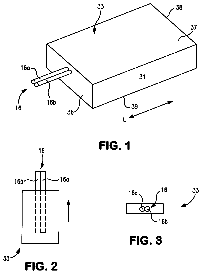
FIG. 1 is a perspective view of the electrochemical device;
FIG. 2 is an arrow II-II cross section of the electrochemical device shown in FIG. 1;
FIG. 3 is an arrow III-III cross section of the electrochemical device shown in FIG. 1;
FIG. 4 is a perspective view of the metallic thin film;
FIG. 5A and FIG. 5B are cross sections of the metallic thin film;
FIG. 6 is a perspective view showing the welding process of the lead body and the metallic thin film;
FIG. 7Aa, FIG. 7Ab, FIG. 7Ac, FIG. 7Ad, FIG. 7Ae, FIG. 7Ba, FIG. 7Bb, and FIG. 7Bc are diagrams showing the method of fixing the lead body and the metallic thin film;
FIG. 8 is a cross section of the circuit board in which the electrochemical device is mounted on the substrate;
FIG. 9 is a diagram explaining the experimental method of the Examples;
FIG. 10 is a diagram explaining the experimental method of Comparative Example 1;
FIG. 11 is a diagram explaining the experimental method of Comparative Example 2;
FIG. 12A, FIG. 12B, FIG. 12C, FIG. 12D, FIG. 12E, and FIG. 12F are diagrams explaining the structure and mounting method of the metallic thin film of the respective Examples;
FIG. 13 is a table showing the experimental results;
FIG. 14 is a circuit diagram showing the internal structure of the electrochemical device;
FIG. 15 is a perspective view of the electrochemical device;
FIG. 16 is an arrow II-II cross section of the electrochemical device shown in FIG. 15;
FIG. 17 is an arrow III-III cross section of the electrochemical device shown in FIG. 15;
FIG. 18 is a perspective view of the metallic thin film;
FIG. 19A and FIG. 19B are cross sections of the metallic thin film;
FIG. 20 is a perspective view showing the welding process of the lead body and the metallic thin film;
FIG. 21A, FIG. 21B, FIG. 21C, and FIG. 21D are diagrams showing the method of fixing the lead body and the metallic thin film;
FIG. 22 is a cross section of the circuit board in which the electrochemical device is mounted on the substrate;
FIG. 23 is a diagram explaining the experimental method of the Examples;
FIG. 24 is a diagram explaining the experimental method of Comparative Example 1;
FIG. 25 is a diagram explaining the experimental method of Comparative Example 2;
FIG. 26A, FIG. 26D, and FIG. 26C are diagrams explaining the structure and mounting method of the metallic thin film of the respective Examples;
FIG. 27 is a table showing the experimental results;
FIG. 28 is a circuit diagram showing the internal structure of the electrochemical device;
FIG. 29A is an XZ cross section SEM photograph in the vicinity of the lead that is fixed to the electrode pad with a solder material, and FIG. 29B is a YZ cross section SEM photograph thereof;
FIG. 30 is a perspective view of the electrochemical device;
FIG. 31 is an arrow II-II cross section of the electrochemical device;
FIG. 32 is an arrow III-III cross section of the electrochemical device;
FIG. 33 is a perspective view of the metallic thin film;
FIG. 34A and FIG. 34B are cross sections of the metallic thin film;
FIG. 35 is a perspective view showing the welding process of the lead body and the metallic thin film;
FIG. 36Aa, FIG. 36Ab, FIG. 36Ac, FIG. 36Ad, FIG. 36Ae, FIG. 36Ba, FIG. 36Bb, and FIG. 36Bc are diagrams showing the method of fixing the lead body and the metallic thin film;
FIG. 37 is a cross section of the circuit board in which the electrochemical device is mounted on the substrate;
FIG. 38 is a diagram explaining the experimental method of the Examples;
FIG. 39 is a diagram explaining the experimental method of Comparative Example 1;
FIG. 40 is a diagram explaining the experimental method of Comparative Example 2;
FIG. 41A, FIG. 41B, FIG. 41C, and FIG. 41D are diagrams explaining the structure and mounting method of the metallic thin film of the respective Examples;
FIG. 42 is a circuit diagram showing the internal structure of the electrochemical device;
FIG. 43 is a perspective view of the electrochemical device;
FIG. 44 is an arrow II-II cross section of the electrochemical device shown in FIG. 42;
FIG. 45 is an arrow III-III cross section of the electrochemical device shown in FIG. 42;
FIG. 46 is a perspective view of the metallic thin film;
FIG. 47A and FIG. 47B are cross sections of the metallic thin film;
FIG. 48 is a perspective view showing the welding process of the lead body and the metallic thin film;
FIG. 49A, FIG. 49B, and FIG. 49C are diagram showing the method of bending the lead and the metallic thin film;
FIG. 50 is a cross section of the circuit board in which the electrochemical device is mounted on the substrate;
FIG. 51A is a cross section of the housing tray, and FIG. 51B is a plan view of the housing tray;
FIG. 52 is a diagram explaining the experimental method of the Examples;
FIG. 53 is a diagram explaining the experimental method of Comparative Example 1;
FIG. 54 is a diagram explaining the experimental method of Comparative Example 2; and
FIG. 55 is a circuit diagram showing the internal structure of the electrochemical device.
Description of the preferred embodiments
The electrochemical device of embodiments according to types A to D is now explained. In the explanation of each type of electrochemical device, the same elements are given the same reference numeral and redundant explanation is omitted. Moreover, the numbers used in the respective Examples are used independently in the explanation of the respective types. The electrochemical device of type A is foremost explained.
FIG. 1 is a perspective view of the electrochemical device, FIG. 2 is an arrow II-II cross section of the electrochemical device, and FIG. 3 is an arrow III-III cross section of the electrochemical device. Moreover, FIG. 8 an XZ cross section of the circuit hoard on which the electrochemical device is mounted.
The electrochemical device 10 includes a charger/discharger 2 housed in an outer package 1, and a plurality of leads 3 extending from the charger/discharger 2. The outer package 1 is configured by superposing a rectangular upper laminated sheet 1A and a rectangular lower laminated sheet 1B, and bonding the areas in the vicinity of the four sides of the periphery thereof. The laminated sheets 1A, 1B are respectively formed by coating an inner surface of an aluminum thin film with a resin layer. A three dimensional Cartesian coordinate system as shown in FIG. 1 is set with the thickness direction of the outer package 1 as the Z axis, the width direction as the Y axis, and the length direction as the X axis. Regions 1Y1, 1Y2 in the vicinity of opposite ends of the outer package 1 in the Y axis direction are bent inward at the boundary line along the X axis, and the mechanical strength of the outer package 1 is thereby enhanced.
An electrolytic solution and the charger/discharger 2 as a battery element are disposed within hermetically-sealed internal space of the outer package 1. Via the lead 3, an electrical charge can be accumulated in the charger/discharger 2 and the accumulated electrical charge can also be discharged therefrom. Various structures may be used for the charger/discharger 2, but capacitors connected in series are used in this example. Specifically, the electrochemical device 10 in this case configures an EDLC (Electric Double Layer Capacitor).
Here, the internal electrical circuit structure of the EDLC is shown in FIG. 14.
The charger/discharger 2 is configured by connecting a capacitor 2A and a capacitor 2B in series, a lead 3.sub.2 is electrically connected to the connection tip parts thereof, and a lead 3.sub.1 and a lead 3.sub.3 are electrically connected, respectively, to terminals which are different from the foregoing connection tip parts of the capacitor 2A and the capacitor 2B. The inside of the outer package 1 is partitioned into two storage parts with a sealant 1S made of polypropylene or the like, and the capacitor 2A and the capacitor 2B are separately housed in the respective storage parts. Electrolytic solutions LQ1, LQ2 are filled in the respective storage parts inside the outer package 1. The respective terminal electrodes configuring the capacitors 2A, 2B are configured by laminating an active material layer and a collector. Moreover, separators S1, S2 as insulating layers are respectively interposed between the respective terminal electrodes configuring the capacitors 2A, 2B. With an EDLC, electrical charges are aligned as a thin layer between the polarizing conductor and the electrolyte (solution), and electrical charge is accumulated by applying a bias therebetween. The center lead 3.sub.2 is used for controlling the potential in the connection tip parts of the capacitors 2A and 2B connected in series.
The active material layer is a polarizing electrode. The polarizing electrode is made of a porous material, and manufactured by mixing binder resin in activated carbon. As the binder resin, used may be a high molecular compound containing fluorine such as polytetrafluoroethylene and polyvinylidene fluoride, a rubber-based high molecular compound such as styrene-butadiene rubber, carboxymethyl cellulose, and so on. As needed, carbon black, carbon nanotubes, graphite particles or microfilaments may be added as a conductive assistant. During the manufacture process, these materials are applied to one side or both sides of the collector.
The collector is made of a metal foil. In addition to using an aluminum foil or a titanium foil with a smooth surface, these may also be used upon subjecting the surface thereof to roughening treatment by way of embossing or etching processing. Note that, as the method of manufacturing an electrode, in addition to the method of adding a conductive supplement and binder to activated carbon and forming a sheet shape and bonding this to the collector, a method of forming the activated carbon into a slurry and applying this to the collector may also be used. As the application method, used may be the applicator method, gravure method, reverse roll method, extrusion (nozzle) method, dip method, and so on.
The separators S1, S2 are formed from a nonwoven fabric or a porous film containing, for example, polyolefin resin at a mass ratio of 10% or more. The polarizing electrode and the separator can also be bonded by applying pressure to a pair of polarizing electrodes under a temperature environment which is not less than the softening temperature of the polyolefin resin. As the separator, cellulose nonwoven fabric or nonwoven fabric of aramid fiber may also be used.
As the electrolytic solution, an aqueous solution and an organic solution are known. As the solvent of an organic electrolytic solution, known are propylene carbonate, ethylene carbonate, dimethyl carbonate, methyl ethyl carbonate, diethyl carbonate, .gamma.-butyrolactone, dimethylformamide, sulfolane, acetonitrile, propionitrile, methoxyacetonitrile and the like, and, as the solute, known are ammonium salt, amine salt, amidine salt and the like.
Returning to FIG. 1 to FIG. 3, the structure of the electrochemical device 10 is explained.
In the electrochemical device 10, the lead 3 comprises a lead body 3A containing Al, and a metallic thin film 3a fixed to the tip of the lead body 3A. The metallic thin film 3a is fixed to the tip part of the lead body 3A, and bent at a side face position of the lead body 3A as the boundary. Moreover, with the example shown in FIG. 1, the metallic thin film 3a covers the upper and lower faces (XY plane) and the side face (YZ plane) of the lead body 3A. In addition, as shown in FIG. 2, predetermined areas (R3U, R3L) of the metallic thin film 3a are welded to the lead body 3A. Note that, although Al is the main component in the lead body 3A, trace amounts of impurities may be contained. The content rate of Al in the lead body 3A is at least 50 mass % or more, and is preferably 95 mass % or more when giving consideration to the electrical conductivity and the resistance properties against the electrolytic solution.
The metallic thin film 3a includes a thin film body 3a1 containing Ni, and a plating layer 3a2 containing Sn and covering at least an outer surface of the bent thin film body 3a1. The predetermined areas to be welded are R3U and R3L. The region to be welded is not the entire area of the metallic thin film 3a, and is only a partial area. Specifically, a specific area (an exposed area which is not covered by the plating layer 3a2 and which includes the predetermined areas R3U, R3L) of the inner surface of the bent thin film body 3a1 and the surface (XY plane) of the lead body 3A are in direct contact without intervention of the plating layer 3a2, and the exposed specific area and the surface of the lead body 3A are welded in the predetermined areas R3U, R3L.
A small space S exists between the inner surface in the vicinity of the bending axis of the metallic thin film 3a, and the lead body 3A, and some of the solder material enters the space S and the connection strength can be increased thereby.
The content rate of Ni in the thin film body 3a1 is at least 50 mass % or more and preferably 95 mass % or more when giving consideration to the point that the adhesion with Al is performed firmly. Moreover, the content rate of Sn in the plating layer 3a2 is decided in consideration of the affinity with the solder material and other matters, but with the electrochemical device of this example, the plating layer 3a2 contains 98.+-.1 (mass %) of Sn and 2.+-.1 (mass %) of Cu..+-.1 (mass %) is a tolerable error. In the foregoing case, there is an ameliorating effect in the solder wettability and the non-growth of whiskers.
The surface of the metallic thin film 3a includes a plating layer 3a2 containing Sn, and the metallic thin film 3a and the electrode pad E1 are fixed firmly via the solder material SD since the wettability with the solder material SD (refer to FIG. 8) is high. The solder material SD of FIG. 8 is in contact with both the plating layer 3a2 and the electrode pad E1. Here, since Ni is contained in the thin film body 3a1 on which the plating layer 3a2 shown in FIG. 2 and FIG. 3 is formed, Ni and Sn are bonded firmly.
Moreover, since the solder material SD of FIG. 8 can crawl up (remain on the upper face when the solder material is caused to drip from above) to the upper face (XY plane in the positive direction of the Z axis) of the outer surface of the bent metallic thin film 3a, the fixation strength between the electrode pad E1 and the metallic thin film 3a can be further increased. Specifically, Al possesses properties of repelling the melted solder material, and, when the side face of the Al lead body 3A is exposed, such exposed face becomes an obstacle and the solder material SD is unable to crawl up any higher, and the solder material SD cannot be applied in the form of being pressed from the upper side. However, with the structure according to the foregoing embodiment, since the Al side face of the lead body 3A is not exposed, the foregoing drawback can be resolved, and a firm fixed state can be formed.
When referring to FIG. 2, although the area in which the plating layer 3a2 of the metallic thin film 3a is not formed (area long the center line CL in the longitudinal direction before bending (refer to FIG. 4)) is welded to the lead body 3A containing Al, since Ni and Al can be welded firmly, the metallic thin film 3a and the lead body 3A are also fixed firmly. Accordingly, it is possible to significantly increase the fixation strength between the electrode pad E1 (FIG. 8) and the lead 3.
Moreover, with the electrochemical device 10 of this example, the metallic thin film 3a is welded to both the upper and lower faces of the lead body 3A as shown in FIG. 2. Thus, since the metallic thin film 3a and the lead body 3A are welded at both the upper and lower faces, the fixation strength thereof can be enhanced.
In addition, when referring to FIG. 2, the dimension Xa of the bent metallic thin film 3a in the longitudinal direction (X axis direction) of the lead is preferably 1 mm or more. If the dimension Xa is less than 1 mm, the bond strength with the electrode pad based on soldering tends to deteriorate, and bond strength required for the connection can be obtained if the dimension Xa is 1 mm or more, especially if it is 2 mm or more Note that the foregoing dimension is preferably 5 mm or less, and sufficient connection strength can be obtained in the foregoing case. Moreover, the ratio ra (=XA/Xa) of the dimension Xa to the dimension XA of the lead 3 from the boundary position with the outer package 1 to the tip position of the lead 3 in the X axis direction is preferably 1.2 or more. If the ratio ra of the dimension is less than 1.2, the lead 3 may come in contact with the outer package and damage the resin layer of the outer package surface, and this tends to increase the short circuit failure rate.
FIG. 4 is a perspective view of the metallic thin film 3a before bending.
To explain the plating layer 3a2 (including the plating layers 3a21, 3a22, 3a23, 3a24, 3a25), strip-shaped plating layers 3a21, 3a22 are formed along the longitudinal direction of the thin film body 3a1 on the inner surface of the thin film body 3a1 (after bending) in the vicinity of the opposite end positions of the bent metallic thin film 3a in the bending axis BL (Y axis) direction (areas in which the width of the metallic thin film 3a in the bending axis BL direction from the respective side faces is within the range of 1% to 20%).
FIG. 5A shows the YZ cross section of the metallic thin film 3a. As a result of forming the plating layers 3a21, 3a22 in the vicinity of the opposite end positions (opposite end positions of the lead in the width direction) in the bending axis BL (Y axis) direction as shown in FIG. 4, the contour of the cross section shape of the plating layer 3a2 (cross section shape that is perpendicular to the longitudinal direction of the lead (YZ cross section)) acquires linearity in comparison to the case (B) of not forming the same. In FIG. 5B, the plating layers 3a21, 3a22 corresponding to FIG. 5A are not formed, and the plating layer in the vicinity of the opposite end positions is rounded and thickened. Meanwhile, with the shape of FIG. 5A, the plating layers 3a23, 3a24 of the side face have a uniform thickness and the contour thereof possesses linearity in the YZ cross section, and are roughly orthogonal to the contour of the plating layer 3a25 on the rear face side. Accordingly, with the shape of FIG. 5A, the product deviation can be reduced since variation in the thickness of the plating layer 3a2 will decrease, and it is thereby possible to provide an electrochemical device of stable quality.
The formation of this kind of plating layer can be performed using methods which are generally well known. The method of forming a plating layer can be generally classified into alkaline, acidic and neutral plating baths.
An alkaline plating bath is configured from potassium stannate or sodium stannate, and potassium hydroxide or sodium hydroxide. When electrodeposition is performed from quadrivalent tin and reaction occurs at a temperature of roughly 70.degree. C., a stable plating layer is formed. Note that the experiments of the Examples described later adopted an alkaline plating bath using an aqueous solution of potassium stannate and potassium hydroxide as the plating solution.
An acidic plating bath is configured from tin sulfate, tin fluoroborate or the like.
Tin chloride is used for a neutral plating bath.
Depending on the degree of adhesion that is required, there are cases of forming copper or nickel plating in a thickness of 1 to 10 .mu.m as the plating surface treatment. As measures against whiskers, there are cases where, after the plating process, melting/heating treatment is preformed or heating is performed at approximately 180.degree. C. for approximately 1 hour.
Moreover, the thickness (average value) of the plating layer 3a2 is 0.5 .mu.m or more and 10 .mu.m or less. Specifically, if the thickness is less than 0.5 .mu.m, defects (pinholes) may arise in the plating layer, and, if the thickness exceeds 10 .mu.m, it tends to interfere with the welding. If the thickness of the Sn plated layer 3a2 is roughly 2 .mu.m, then the solder wettability becomes favorable. The solder wettability is defined, for example, based on the standard (JESD22-B102E) of the reliability test of individual semiconductor electronic components conducted by the standardization organization Solid State Technology Association (JEDEC). With a tin plating layer formed on a thin film prepared under the foregoing conditions, a solder layer can be formed on 95% or more of the solder dipping area based on the following conditions; for instance, soldering temperature of 245.degree. C., dip speed of 1.8 mm/sec, dip time of 3 seconds, and dip depth of 2 mm.
Moreover, in cases where the thickness of the Ni thin film body 3a1 is approximately 100 .mu.m, if the thickness of the Sn plated layer 3a2 exceeds 10 .mu.m, the bending portion is subject to stress and there are case where cracks occur at the interface of the Ni thin film body 3a1 and the Sn plated layer 3a2. These cracks tend to deteriorate the bond strength. Moreover, whiskers tend to arise when much stress remains in the Sn plated layer 3a2, and, consequently, a short circuit tends to occur in the vicinity of the terminal. As a result of mounting the metallic thin film 3a including the Sn plated layer 3a2 on the Al lead body 3A, the solder wettability (fillet formability) can be improved significantly.
In addition, the thickness of the thin film body 3a1 is preferably 50 .mu.m or more and 500 .mu.m or less. If the thickness of the thin film body 3a1 falls below 50 .mu.m, in the case of forming the foregoing plating layer structure, an adhesive tape is affixed to the non-plated area (area along the center line CL in FIG. 4) of the thin film body 3a1, plating is subsequently performed, and the adhesive tape is peeled thereafter at an appropriate timing, but the thin film body 3a1 oscillates during the foregoing process and wrinkles, kinks, crimps and the like tend to form on the thin film body, and, since such defects cannot be controlled, an error occurs in the quality of the product. Moreover, if the thickness of the thin film body 3a1 exceeds 500 .mu.m, this is undesirable since a phenomenon occurs where bonding with the lead becomes difficult. The present invention can inhibit the foregoing defects by setting the thickness of the thin film body to be within the foregoing range.
As described above, since the bonding (ultrasonic fusion) of the Ni tab (metallic thin film) of the Sn plated surface and the Al lead body 3A is difficult, plate processing is not performed to the bonding plane. Although it is advantageous to cover the entire side face of the metallic thin film 3a with the Sn plated layer in terms of forming a fillet, a certain level of effect can be yielded even if the Ni substrate is exposed. The Sn plate processing is performed in succession and a required amount (for example, roughly 20 mm) is used by being cut before being bonded to the Al lead body 3A. Thus, although the Sn plated layer does not exist in the cut plane, there is no problem since this portion does not affect the formation of a fillet.
FIG. 8 is the XZ cross section of the circuit board which is configured by the foregoing electrochemical device 10 being mounted on a substrate. In order to clarify the features, the portion of the outer package 1 is shown as a side face and not as a cross section.
This circuit board comprises a substrate SB comprising an electrode pad E1 and on which the electrochemical device 10 is mounted. The main material of the substrate SB is an insulating material, and the electrode pad E1 is formed on the surface thereof. Various electronic components can be mounted on the substrate SB, but this example only shows the portion of the electrochemical device 10, which is the feature of this example.
This circuit board comprises a double-sided adhesive tape 4 which is interposed between the rear face of the outer package 1 and the substrate SB, and a solder material SD which is interposed between the electrode pad E1 and the metallic thin film 3a, and which reaches an outer upper face of the metallic thin film 3a.
In the foregoing case, as described above, since the lead 3 and the electrode pad E1 are firmly fixed and the rear face of the outer package 1 and the substrate SB are also firmly fixed with the double-sided adhesive tape 4, obtained is a circuit board that is resistant to oscillation.
Moreover, with this circuit board, the solder material SD contains Sn and Cu. Since this kind of material has favorable affinity with Sn contained in the plating layer 3a2 (refer to FIG. 4), the wettability of the solder material SD will increase. However, since Cu is contained, the melting point of the solder decreases, and effects are yielded in that the solder workability is improved and the solder wettability is improved. Moreover, the solder material more preferably contains trace amounts of Ag. In the foregoing case, an effect is yielded in that the durability after the solder welding will improve. The ratio (mass percent ratio) of the respective elements in the solder material SD in this example is as shown below, and a variation of .+-.1 (mass %) is tolerated in the respective numerical values (provided, however, that the ratio of Cu>0 mass %).
Sn:Cu:Ag=96.5 (mass %):0.5 (mass %):3 (mass %)
The method of assembling the foregoing lead is now explained.
FIG. 6 is a perspective view showing the welding process of the lead body and the metallic thin film.
The lead body 3A and the metallic thin film 3a are prepared, and areas are partially superposed so that the longitudinal directions thereof coincide with the X axis. The width Y2 of the lead body 3A in the Y axis direction, the width Y1 of the metallic thin film 3a, and the width Y0 of the welding area R3U are constant along the X axis, but the width Y0 of the welding area R3U is smaller than the width Y2 of the lead body 3A, and, as a general rule, the welding area R3U does not overlap with the plating layers 3a21, 3a22 (refer to FIG. 4) positioned at the opposite ends in the Y axis direction.
The width Y2 of the lead body 3A in the Y axis direction is smaller than the width Y1 of the metallic thin film 3a, and, although the width Y2 of the lead body 3A is shorn to be smaller than the width. Y1 of the metallic thin film 3a in FIG. 6, these widths may also be the same. Ultrasonic vibrator heads 20, 21 for performing ultrasonic welding are positioned at the vertical position in the thickness direction, and, by oscillating an oscillator that is mechanically connected to at least one of such ultrasonic vibrator heads 20, 21, the welding area R3U that comes into contact with the ultrasonic vibrator heads 20, 21 will melt, and the lead body 3A made of Al and the lower face exposed area (Ni) of the metallic thin film 3a become fused.
FIG. 7 is a diagram showing the method of fixing the lead body and the metallic thin film.
As the foregoing fixing method, considered may be the method shown in FIG. 7Aa to FIG. 7Ae (hereinafter referred to as the "bend-type manufacturing method") and the method shown in FIG. 7Ba to FIG. 7Bc (hereinafter referred to as the "cover-type manufacturing method").
The method (A) is foremost explained. The process shown in FIG. 6 is illustrated in FIG. 7Aa. In this process, the lead body 3A and the metallic thin film 3a are subject to ultrasonic welding and thereby physically and electrically connected. Next, as shown in FIG. 7Ab, the lead body 3A and the metallic thin film 3a are pinched with jigs 23, 22, and, as shown with the arrow of FIG. 7Ab, the metallic thin film 3a that is protruding from the jigs is bent with the Y axis as the bending axis. The positive direction end of the X axis of the jigs 23, 22 is parallel to the Y axis, and these positive direction ends coincide with the position of the positive direction end of the X axis of the lead body 3A. The cross section shape of the lower jig 23 is a right triangle in the XZ plane, and its inclined face is inclined so as to form an acute angle relative to the X axis (angle of the jig is 90 degrees or less (particularly around 30 degrees)).
Accordingly, when the metallic thin film 3a is bent by being pressed against the inclined face of the jig 23, as shown in FIG. 7Ac, the metallic thin film 3a is bent with the Y axis as the bending axis. Next, as shown in FIG. 7Ad, by removing the lower jig 23 and pressing the floating metallic thin film 3a in the direction (Z axis positive direction) of the arrow in FIG. 7Ad, the metallic thin film 3a will become completely bent and contact the rear face of the lead body 3A. Finally, as shown in FIG. 7Ae, the lead body 3A and the metallic thin film 3a are subject to ultrasonic fusion once again. This ultrasonic fusion process is the same as the process shown in FIG. 6 and FIG. 7Aa excluding the point that the metallic thin film 3a is bent. Based on the foregoing process, the lower welding area R3L (refer to FIG. 2) is formed, the thin film body 3a1 of the metallic thin film 3a and the lead body 3A are welded, and these become physically and electrically connected.
Note that, in the foregoing process, although the bending axis of the metallic thin film 3a is parallel to the Y axis in FIG. 7, this may also be parallel to the X axis as described later.
The description continues in the full USPTO document.
 Lapsed, fee not paid5 drawings