The invention relates to a new High Electron Mobility Transistor (HEMT), made essentially of layers of Group XIII element(s) nitrides(s). The invention relates also to a method of manufacturing of High Electron Mobility Transistor (HEMT).
First field effect transistors (Metal Oxide Semiconductor Field Effect Transistor, MOSFET) were constructed in late 1970's in Fujitsu laboratories (Mimura, Yokoyama, 1977). They were based on gallium arsenide. Due to higher switching speed, high linearity of signal and other favorable properties, MOSFETs were soon applied in low-noise amplifiers, used mainly in telecommunications. Intensive research directed at systematical improvement of transistors of this type led to construction of High Electron Mobility Transistors (HEMT), in which modern semiconductor materials, such as e.g. gallium nitride or aluminum nitride, are used.
The HEMTs are still mainly used in ground and space communication systems, in particular in satellite telecommunication and television, cellular networks, GPS systems, radiotelescopes and modern radars (phased array radars).
Currently, LDMOS-type (Lateral Diffused Metal-Oxide-Semiconductor) systems, based on silicon, are prevalent in the above-mentioned applications. For example, they constitute 90% of the transistors used in BTS's (base transceiver stations) in cellular telephony. This is mainly due to economic reasons, as LDMOS systems are relatively inexpensive (cheaper both than nitride and gallium arsenide HEMTs, due to the advanced technology and mass manufacturing of those systems) and are characterized by a long mean time to failure (MTTF). Moreover, the position of LDMOS systems as a leader in this area is aided, on one hand, by "inertia" of their recipients (i.e. manufacturers of power amplifiers) and, on the other hand, by the systematic improvement of the parameters of those systems, for example towards achieving higher outputs, higher frequencies, and ability to operate at higher temperatures--appropriately to the needs of the developing communication technologies.
However, it is expected that in the near future a dynamic development of wireless fast data transmission networks (3-rd generation cellular networks) is very likely, e.g. in the W-CDMA standard (Wideband Code-Division Multiple-Access), which uses a signal with the frequency of approx. 2 GHz. Work is also underway on the development of communication techniques in X-Band, i.e. 8-12 GHz. Such networks create a huge demand for modern transistors as well as high-power and high-frequency amplifiers which must be characterized by a perfect linearity of the signal (i.e. produce an amplified signal that is, for all practical purposes, free of any distortions), reliability, and stability of operating parameters in an extended period of time. Preferably, the equipment that is being used should be able to operate under the conditions of varying power output (in the W-CDMA networks the power output indeed varies depending on the traffic density) and a high peak-to-mean mode. Meanwhile, LDMOS systems have proved most useful under stable conditions and with limited power output thus do not meet the parameters required by the new technology. Such requirements can be easier fulfilled by constructing devices that are able to operate under higher voltages, since in the case of present LDMOS structures an increase in voltage results in lower amplification and considerably faster degradation of equipment, whose operation becomes less stable after an extended period of time. In summary, the dominating position of LDMOS systems is currently more due to economic reasons than to their parameters and performance. Consequently, their position may be lost, if they do not satisfactory fulfill technical demands of the currently-developed new communication techniques.
On the other hand, all those requirements are perfectly fulfilled by HEMT structures built of Group XIII element(s) nitride(s), particularly gallium nitride and aluminum nitride. Gallium nitride is characterized by the breakdown voltage higher by one order of magnitude than that of GaAs, as well as higher thermal resistance. Therefore, nitride HEMT transistors can work at higher voltages, which considerably facilitates designing the discussed systems under development. Smaller dimensions of individual parts, particularly gates (as compared with the currently available devices) allow to achieve higher switching rates, thus allowing to amplify the signals with higher frequencies and expand the available band widths. Due to the high thermal resistance of nitrides, the HEMT transistors that are built of nitrides can work at high temperatures, which in turn allows to achieve power output density that is several times higher than that of the devices available on the market. Additionally, nitride structures are characterized by a linearity of the signal, ability to achieve a high power output, and stability of operating parameters throughout an extended period of time. For example, extrapolation of the measurements of electric parameters of a nitric HEMT device made by Nitronex (obtained on a silicon substrate) suggests that those parameters will change by less than 10% in 20 years ("Compound Semiconductor", no. 6, 2004, page 31).
The aforementioned advantages translate into direct benefits resulting from the application of nitride HEMT structures, particularly in modern communication techniques, including 3-rd generation cellular communication networks. In practical terms, the ability to work at higher voltages and achieve higher power outputs and higher amplification means less amplification stages, and thus simpler, smaller, and lighter amplification systems (less transistors in an amplifier). On the other hand, the ability to work in a wide scope of frequencies allows to use a single nitride transistor for three communication bands (e.g. PCS, DCS, UMTS) instead of the several currently available LDMOS systems. Finally, the ability to operate HEMT structures at higher temperature and in the presence of stronger electric fields allows to significantly reduce or even entirely eliminate the necessity to cool amplifier systems. Consequently, it is expected that those systems will become smaller and lighter, as well as less expensive to manufacture and operate. In the case of cellular base transceiver stations it will be possible to place the amplifier and the antenna closer to each other, thus allowing to reduce signal transmission losses (which currently reach approx. 50%), and enabling tower-top mounting of amplifiers (in direct proximity of the antenna). Smaller and lighter amplifier systems that do not require cooling will prove very competitive in satellite telecommunication. It is also possible to construct super low-noise amplifiers that could be used in radio telescopes or modern radars.
The above discussed expected advantages of using nitride devices affect the level of intensity of the research aimed at developing an appropriate HEMT structure, as well as its manufacturing method that could be applied in industry and be economically competitive. Currently HEMT structures are produced on several types of substrates using epitaxial methods (e.g. MOCVD, MBE). The basic problem consists in the lack of appropriate nonconductive homosubstrates for obtaining such structures (e.g. substrates of bulk gallium nitride), since the sufficiently big nitride monocrystals that could be used to produce such substrates were not thus far available. Therefore, it is necessary to use foreign substrates (heterosubstrates)--e.g. of sapphire, silicon, or SiC--where an appropriate nucleation layer is deposited directly onto the substrate, followed by (optionally) a buffer layer, and only then the proper nitride layers are deposited on that layer. However, the use of a heterosubstrate is not an optimal solution, because irrespective of the type of heterosubstrate and the employed technique of manufacturing HEMT devices, the crystalline lattice mismatch and different thermal expansion coefficients of the substrate and of the nitride layers deposited on it become the source of tensions and defects in the obtained material, which causes a dramatic deterioration of the structure, quality and performance of the manufactured devices. Moreover, sapphire substrates are not suitable for high power electronics (due to the relatively low thermal conductivity of sapphire). In this respect, SiC substrates are better, although the technologies used to obtain such substrates are not sufficiently developed as yet, making those substrates expensive to produce. Further problem is SiC doping, required to obtain a compensated (semi-insulating) material. Recently there have been reports on Fujitsu constructing a HEMT transistor on a conductive SiC substrate, on which a thin (10 .mu.m) AlN layer was produced using the HVPE method (http://compoundsemiconductor.net/articles/news/8/12/21). Although this invention eliminates the necessity of using compensated SiC, it does not solve all the other problems caused by the usage of heterosubstrate. Moreover, in this case the known problem of "parasitic conduction" occurs. The parasitic conduction is the result of generation of free carriers on the AlN/SiC interface (eg. S. C. Binari, D. S. Katzer, D. F. Storm, B. V. Shanabrook, E. R. Glaser, and J. A. Roussos, "Molecular Beam Epitaxial Growth of AlGaN/GaN High Electron Mobility Transistors", in 2003 US Naval Research Laboratory Review). Creating of an additional ("parasitic") channel for current flow between the source and the drain considerably deteriorates the parameters of the HEMT transistor. Other known HEMT devices are produced on silicon substrates (Nitronex, Micro GaN) or compensated SiC substrates (Rockwell Scientific Company, RF Micro Devices, Eudyna Devices/Fujitsu). Let us however repeat, that in every such case, the mismatch between the substrate and the epitaxial layers deteriorates the crystalline quality and electrical parameters of a HEMT structure obtained by heteroepitaxy.
Experiments show that a better structural quality of the AlGaN/GaN interface results in a favorable increase in the mobility of carriers within the active area of the device. Moreover, it is known that the quality and performance of HEMT transistors improve with the quality of epitaxial layers ("Journal of Applied Physics", vol. 87, no. 1, 2000, pages 334-344). Currently, the main aim of the research worldwide is to minimize undesired effects resulting from substrate's mismatch, i.e. to provide such a substrate, nucleation layer or the HEMT structure which "levels"--to a possibly largest extent--the disadvantageous influence of the substrate on the crystalline quality of heteroepitaxial layers. In particular, it is expected that--in each of the above cases--it would be possible to obtain considerably better HEMT structures with even better operating parameters, provided that those structures can be produced on homosubstrates, but this possibility has not been--up to now--seriously considered, due to a lack of an industrially applicable method of manufacturing satisfactory compensated homosubstrates.
Moreover, it should be noted that the available heterosubstrates limit the production of HEMT structures to those with AlGaN/GaN interface coinciding with the polar plane C of the nitride crystalline lattice. According to numerous publications, further desired improvement in the performance of nitride HEMT transistors could be achieved by producing them using homosubstrates with non-polar surface (e.g. surface coinciding with the non-polar plane A or M of the nitride crystalline lattice). Consequently, another aim of the research around the world is to provide substrates for epitaxial deposition of nitride layers, having the desired polarity and/or orientation with respect to the crystalline lattice of gallium nitride. In particular, such substrates can be produced from the gallium-containing nitride monocrystals of appropriate size.
Currently used industrial technologies of obtaining nitride monocrystals are not satisfactory as they do not allow to obtain crystals of appropriate size and quality, or their efficiency and industrial applicability is limited.
Some available epitaxial methods, such as for example the MOCVD, HVPE or MBE methods, can be used to produce GaN substrates with the diameter of up to two inches, but they are seriously limited due to the lack of appropriate substrates (particularly nitride homosubstrates). Thus obtained material is characterized by surface dislocation density of at least approx. 10.sup.8/cm.sup.2 or approx. 10.sup.7/cm.sup.2 if the Epitaxial Lateral Overgrowth (ELOG) method is applied simultaneously. Such dislocation density is much too high for its possible application for producing HEMT transistors. Additionally, the achieved growth rates make it impossible to obtain a true bulk crystal.
The standard methods of crystallization from melt and the sublimation methods cannot be applied due to the decomposition of nitrides into metals and N.sub.2.
In the HNP method such decomposition is inhibited by using the atmosphere of high nitrogen pressure (it is necessary to apply temperatures of approx. 1500.degree. C. and pressures of approx. 1500 MPa, which constitutes a serious limitation considering the bigger scale and industrial applicability of the process). In this way, it is possible to obtain GaN wafers with the dimensions of approx. 10 mm. So far, it has been impossible to achieve seeded growth of gallium nitride using that method. The obtained crystals are the result of the uncontrolled process of spontaneous growth, causing numerous defects in the obtained crystals, such as twinning, edge and screw dislocations, etc.
Promising results were obtained from the application of flux growth methods to obtain gallium-containing nitrides from gallium alloys in the atmosphere of nitrogen. These methods are attractive for industry because of the application of relatively low temperatures and low pressures, although as of now, the FLUX methods are yet to leave the laboratory stage of research. Similarly to the HNP method, the main problem is how to achieve a controlled seeded growth. The first seeding attempts in FLUX processes were presented only in the last few months at several scientific conferences.
U.S. Patent Application Publication No. 2006-0037530 A1 related to International Publication No. WO2004/053206 and U.S. Pat. No. 7,314,517 related to International Publication No WO2004/053208 disclose the method of obtaining bulk monocrystalline gallium-containing nitride by crystallization from supercritical ammonia-containing solution containing alkali metal ions. The characteristic feature of bulk nitride monocrystals obtained using the above-mentioned supercritical ammonia-containing solution is their low dislocation density (approximately 10.sup.4/cm.sup.2), high electric resistivity (in the case of undoped bulk GaN--several .OMEGA.cm), as well as high crystalline quality (half width of the X-ray rocking curve (FWHM) from the
plane below 60 arcsec--for the Cu K .alpha..sub.1 line). Moreover, U.S. Patent Application Publication No. 2006-0037530 A1 and U.S. Pat. No. 7,314,517, both of which are incorporated by reference, disclose that the monocrystals contain Group I elements, in a concentration of at least 0.1 ppm.
Recently a method was developed to obtain gallium-containing nitride monocrystals grown on the seed, essentially without propagating the crystalline defects occurring on the seed. This method was disclosed in the Polish patent applications nos. P-368483 (dated Jun. 11, 2004) and P-368781 (dated Jun. 25, 2004), which have not been published yet. It involves growing a crystal on the seed at least in the direction essentially perpendicular to the direction of the growth of the seed. This method can be used to obtain large bulk monocrystals (3 cm and larger) with exceptionally favorable quality parameters (surface dislocation density preferably approx. 10.sup.2/cm.sup.2, curvature radius of the crystalline lattice preferably approx. 70 m, and half width of the X-ray rocking curve (FWHM) from the
plane preferably below 40 arcsec (for the Cu K .alpha..sub.1 line). Due to the considerable sizes of the obtained crystals it is possible--as needed--to use them to obtain substrates for epitaxy of the desired orientation and polarity (e.g. with the surface coinciding with the polar plane C, or with the surface coinciding with the non-polar plane A or M of the crystalline lattice of gallium-containing nitride). Thus, from the viewpoint of crystalline structure, these are optimal substrates for manufacturing of nitride electronic devices. However, there was still the problem of obtaining an insulating substrate, because--as mentioned above--the thus obtained gallium-containing nitride has the electric resistivity of the order of several .OMEGA.cm, far too low from the viewpoint of manufacturing HEMT structures. Doping attempts, in which the acceptor-type dopants, as e.g. zinc or magnesium, were introduced into the environment of the process, encountered technological obstacles. The presence of said elements in the environment of the process according to the disclosure of WO2004/053206 and WO2004/053208 resulted in a dramatic drop of the growth rate of nitride crystals, and consequently monocrystals of desired size could not be obtained within a reasonable time. Unexpectedly, these obstacles have been overcome by optimizing the parameters of the crystallization process, such as pressure and the temperature distribution, as well as appropriate preparation of feedstock.
It was now unexpectedly discovered that the process of controlled doping of the bulk monocrystals grown as described above at a certain level allows to obtain compensated (semi-insulating--with resistivity of approximately 10.sup.6.OMEGA.cm) material, which gave the inventors an incentive to take up research aiming at using this material to produce homosubstrates for nitride HEMT transistors with optimal quality and electric conductivity (from viewpoint of that particular application).
Therefore, the objective of this invention is to provide HEMT transistors built of layers of gallium-containing nitride deposited in nitride homosubstrate. Another objective of this invention is to provide a method of manufacturing of said HEMT transistors.
According to the invention, the High Electron Mobility Transistor (HEMT), made essentially of layers of Group XIII element(s) nitride(s) (IUPAC, 1989), is formed on a substrate of gallium-containing nitride, made of a single crystal obtained by crystallization from supercritical ammonia-containing solution.
Preferably, the transistor according to the invention is produced on a substrate formed of a single crystal obtained by growth on a seed, at least in the direction essentially perpendicular to the direction of the growth of the seed.
A semi-insulating (compensated) substrate is preferably used to produce the transistor according to the invention.
According to the invention, the transistor is produced on a polar substrate.
Alternatively, the transistor according to the invention is produced on a non-polar substrate.
Preferably, in the transistor according to the invention, the buffer layer is deposited directly on the substrate.
The transistor according to the invention has mean output power in the W-CDMA band (ca. 2 GHz) preferably not lower than 50 W, while the gain is preferably not lower than 25 dB at 60V.
According to the invention, at least the buffer layer is produced by epitaxial methods and the direction of growth of said layer in the epitaxial process is essentially perpendicular to the direction of growth of the substrate.
The invention covers also a method of manufacturing of said HEMT transistors, in which at least the buffer layer is produced by epitaxial methods and the direction of growth of said layer in the epitaxial process is essentially perpendicular to the direction of growth of the substrate.
The HEMT transistors produced on such substrates using epitaxial methods have exceptionally favorable performance parameters (for example, mean output power in the W-CDMA band (ca. 2 GHz)--50 W, gain 25 dB at 60V). They can work in a stable manner at a higher voltage as well as higher power and signal frequencies than the aforementioned known HEMT devices, and it is possible to achieve even a higher amplification. The problem of parasitic conduction is absent in this case.
As the problem of lattice constant mismatch and different thermal expansion coefficients of the substrate and the layers deposited thereon is absent as well--the epitaxial layers, being parts of the HEMT structure according to the invention, are of high quality. It turned out that even further improvement of parameters of the manufactured devices is possible, provided that the epitaxial layers are grown in the direction essentially perpendicular to the direction of growth of the substrate.
Of course, the use of a homosubstrate does not solve all possible technical problems, which may occur in a HEMT structure. Some of the known problems are not a direct consequence of the use of a heterosubstrate and they may appear also in the transistor according to the invention. Such problems should be solved in appropriate way, known to those skilled in the art and in particular--by appropriate modification of the HEMT structure. Thus, the inventive transistor may be modified in order to obtain further improvement of its parameters. High gate leakage current may be used as the example. It was discovered (P. D. Ye et. al., Appl. Phys. Lett. 86 063501), that this current can be reduced by about six orders of magnitude by placing a thin dielectric layer (e.g. Al.sub.2O.sub.3 or HfO.sub.2) below the gate. Of course, similar modification may be applied in the HEMT structure according to the invention.
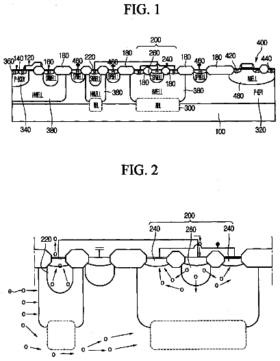
The present invention is illustrated by the accompanying drawings in which:
FIG. 1 shows a scheme of a known HEMT structure,
FIG. 2 shows a scheme of a HEMT structure according to the invention,
FIG. 3 shows the change of temperature in time in a process described in Example 1 and
FIG. 4 shows the change of temperature in time in a process described in Example 2.
Any technical terms used throughout the specification and the claims related to the present invention should be construed according to the definitions given below:
Group XIII element-containing nitride means a nitride of Group XIII element(s) (IUPAC, 1989), i.e. aluminum, gallium and indium either alone or in any combination. Gallium-containing nitride is the most preferred such nitride.
Gallium-containing nitride is a chemical compound containing in its structure at least one atom of gallium and one atom of nitrogen. It includes, but is not restricted to, a binary compound--GaN, a ternary compound--AlGaN, InGaN or a quaternary compound AlInGaN, preferably containing a substantial portion of gallium, anyhow at the level higher than dopant content. The composition of other elements with respect to gallium in this compound may be modified in its structure insofar as it does not collide with the ammonobasic nature of the crystallization technique.
A substrate of bulk mono-crystalline gallium-containing nitride means a monocrystalline substrate of gallium-containing nitride, on which electronic devices such as HEMT may be obtained by MOCVD method or by the methods of epitaxy growth such as HVPE, wherein its thickness is preferably at least 200 .mu.m, more preferably at least 500 .mu.m.
Homosubstrate means a substrate made of the same crystal as the layers deposited on this substrate. For example, when a substrate made of gallium nitride is used for epitaxial deposition of gallium nitride layers, then this substrate is called a homosubstrate.
Heterosubstrate means a substrate made of a crystal different from the layers deposited on this substrate. For example, when a substrate made of sapphire is used for epitaxial deposition of gallium nitride layers, then this substrate is called a heterosubstrate.
Precursor of gallium-containing nitride is a substance or a mixture containing at least gallium and optionally containing elements of Group I (alkali metals), elements of Group II (alkali earth metals), elements of Group XIII (group numbers according to IUPAC 1989), nitrogen and/or hydrogen, and metallic gallium, its alloys or metallic compounds, hydrides, amides, imides, amido-imides and azides, which may form gallium compounds soluble in the supercritical ammonia-containing solvent as defined below.
Gallium-containing feedstock is gallium-containing nitride or its precursor. As a feedstock, GaN obtained by various methods may be used, among others by flux methods, HNP method, HVPE method or poly-crystalline GaN obtained by reaction of metallic gallium with supercritical ammonia-containing solution.
Supercritical ammonia-containing solvent is a supercritical solvent consisting at least of ammonia, which contains one or more types of Group I elements (alkali metals), supporting dissolution of gallium-containing nitride. Supercritical ammonia-containing solvent may also contain derivatives of ammonia and/or mixtures thereof, in particular--hydrazine.
Mineralizer is a substance introducing into the supercritical ammonia-containing solvent one or more Group I element (alkali metal) ions, supporting dissolution of feedstock.
Dissolution of gallium-containing feedstock means either reversible or irreversible process of forming--out of said feedstock--gallium compounds soluble in the supercritical solvent, for example gallium-complex compounds. Gallium complex compounds are complex chemical compounds, in which an atom of gallium is a coordination center surrounded by ligands, such as ammonia molecules (NH.sub.3) or their derivatives, like NH.sub.2.sup.-, NH.sup.2-, etc.
Supercritical ammonia-containing solution means a solution obtained as the result of dissolution of gallium-containing feedstock in the supercritical ammonia-containing solvent.
Solubility
Our experiments show that the state of equilibrium may be achieved between the solid (gallium-containing nitride) and the supercritical solution at sufficiently high temperature and pressure. Therefore, the solubility of gallium-containing nitride may be defined as the equilibrium concentration of gallium-complex compounds obtained in the above mentioned process of dissolution of gallium-containing nitride. In this process, the equilibrium concentration, i.e. solubility, may be controlled by changing the composition of solvent, temperature and/or pressure.
Temperature and Pressure Coefficient of Solubility (TCS and PCS)
Negative temperature coefficient of solubility means that the solubility is a decreasing function of temperature if all other parameters are kept constant. Similarly, positive pressure coefficient of solubility means that, if all other parameters are kept constant, the solubility is an increasing function of pressure. Our research allows to state that solubility of gallium-containing nitride in the supercritical ammonia-containing solvent, at least in the temperature range from 300.degree. C. to 550.degree. C., and pressure from 100 MPa to 550 MPa, shows a negative temperature coefficient (negative TCS) and a positive pressure coefficient (positive PCS).
Supersaturation
If the concentration of soluble gallium compounds in the supercritical ammonia-containing solution is higher than the solubility of gallium-containing nitride in specific physico-chemical conditions, then the supersaturation of the supercritical ammonia-containing solution with respect to gallium-containing nitride in those conditions can be defined as the difference between the actual concentration and the solubility. While dissolving gallium-containing nitride in a closed system it is possible to obtain the supersaturation state, for example by increasing temperature or decreasing pressure.
Chemical transport of gallium-containing nitride in the supercritical solution means a continuous process involving dissolution of a gallium-containing feedstock in the supercritical solution, circulation of the gallium-complex compounds within the solution and crystallization of gallium-containing nitride from the supersaturated supercritical solution. Generally, chemical transport may be caused by temperature difference, pressure difference, concentration difference, or other chemical or physical differences between the dissolved feedstock and the crystallization product. Bulk monocrystalline gallium-containing nitride may be obtained in effect of chemical transport between the dissolution and crystallization zones of the autoclave, established by means of temperature difference between the two zones, whereas the temperature in the crystallization zone should be higher than the temperature in the dissolution zone.
Seed is crucial for obtaining a desired bulk gallium-containing nitride monocrystals by crystallization from supercritical ammonia-containing solution. In view of the fact that the quality of the seed is crucial for the crystalline quality of the bulk gallium-containing nitride monocrystals, the seed selected for the process should have possibly high quality. Various structures or wafers having a modified surface can also be used. For example a structure having a number of surfaces spaced adequately far from each other, arranged on a primary substrate and susceptible to the lateral overgrowth of crystalline nitrides may be used as a seed (ELOG structures). Seeds can be produced using various methods, e.g. by growth from gaseous phase, such as HVPE, MOCVD or MBE.
HVPE (Halide Vapor Phase Epitaxy) method refers to a method of deposition of epitaxial layers from gaseous phase, in which (in the case of nitrides) halides of metals and ammonia are used as substrates.
MBE (Molecular Beam Epitaxy) method refers to a method of obtaining epitaxial layers of atomic thickness by depositing molecules from a so-called "molecular beam" on a substrate.
MOCVD (Metallo-Organic Chemical Vapor Deposition) method refers to a method of deposition of epitaxial layers from gaseous phase, in which (in the case of gallium nitride) ammonia and metallo-organic compounds of gallium are used as substrates.
Spontaneous crystallization from the supersaturated supercritical ammonia-containing solution means any undesirable process of nucleation and growth of the gallium-containing nitride crystals taking place at any site within the autoclave except on the surface of the seed. The definition also includes growth on the surface of the seed, in which the grown crystal has an orientation different from that of the seed.
Selective crystallization on a seed means a process of crystallization taking place on the surface of the seed, in the absence of spontaneous crystallization or with spontaneous crystallization occurring in a negligible degree. This process is indispensable for obtaining bulk monocrystals of gallium-containing nitride.
Temperature and Pressure of the Reaction
In the practical example presented in the present specification temperature measurements inside the autoclave have been performed when the autoclave was empty, i.e. without the supercritical ammonia-containing solution. Thus, the temperature values cited in the examples are not the actual temperature values of the process carried out in the supercritical state. Pressure was measured directly or calculated on the basis of physical and chemical data for ammonia-containing solvent at selected process temperature and the volume of the autoclave.
Autoclave, regardless of its from, includes a closed reaction chamber, in which the ammonobasic crystallization process is carried out.
Crystallographic directions c, a or m refer to c, a or m directions of hexagonal lattice, having the following Miller indices: c--[0001], a--[1 1 2 0], m--[1 1 00].
Crystallographic planes C, A or M refer to C-, A- or M-plane surfaces of hexagonal lattice, having the following Miller indices: C--(0001), A--(1 1 2 0), M--(1 1 00). The surfaces are perpendicular to the corresponding crystallographic directions (c, a and m).
The direction of growth of the seed is the direction of growth of the crystal, out of which the seed used in this method was made. This direction is determined by the method used to produce the seed. At the same time, this is the main direction of propagation of dislocations in the seed. For example, GaN wafers obtained by HVPE method can be used as seeds in the process of GaN growth by crystallization from supercritical ammonia-containing solution. In the HVPE method, the wafers are grown essentially in the c direction of the gallium nitride hexagonal lattice. Thus, in this case the c direction is the direction of the growth of the seed.
The direction of growth of the substrate is the direction of growth of this part of the crystal, out of which the substrate was made. At the same time, this is the main direction of propagation of dislocations in the substrate. It turns out that epitaxy process, in which the epitaxial layers are grown in the direction essentially perpendicular to the direction of growth of the substrate, results in the layers of a very high quality, as the defects present in the substrate do not propagate in such layers.
Group XIII Element-Terminated Side, Ga-Terminated Side, N-Terminated Side:
In the crystals having the wurtzite structure one can distinguish a crystalline direction (crystalline axis) denoted as c, parallel to the C.sub.6 symmetry axis of the crystal. In the crystals of Group XIII element nitrides, having the wurtzite structure, the crystalline planes perpendicular to the c axis (C-planes) are not equivalent. In is a habit to call them Group XIII element-terminated side and nitrogen-terminated side or the surface having Group XIII element polarity or nitrogen polarity, respectively. In particular, in the case of monocrystalline gallium nitride one can distinguish gallium-terminated side (Ga-side) and nitrogen-terminated side (N-side). These sides have different chemical and physical properties (eg. susceptibility to etching or thermal durability). In the methods of epitaxy from the gaseous phase the layers are deposited on the Group XIII element-terminated side.
ELOG (Epitaxial Lateral Overgrowth) is a method of crystal growth from gaseous phase or from supercritical ammonia-containing solution, in which crystals are grown on a special substrate. In the case of gallium nitride crystals, a matrix of parallel ridges (several microns high and several microns wide), having surfaces susceptible to lateral growth, is created on the surface of the substrate. Typically, gallium nitride crystals are grown in the c direction. The ridges are then created along the m direction and the surfaces susceptible to lateral growth coincide with A-planes. In this case, lateral growth is limited to several or several dozen microns and it is finished as soon as the space between the ridges becomes overgrown by the arising crystal. Next, the principal growth of bulk crystal proceeds along the c direction. This way some of the dislocations present in the substrate can be prevented from penetrating into the arising crystal.
Lateral growth in this patent application refers to bulk growth on a seed in the direction perpendicular to the original direction of the growth of the seed. In contrast to ELOG (Epitaxial Lateral Overgrowth), the lateral growth is definitely macroscopic (of the order of dimensions of the seed or even larger). Moreover, the projection of a laterally grown crystal in the direction parallel to the original direction of seed growth goes remarkably beyond the projection of the seed used. In the case of ELOG (Epitaxial Lateral Overgrowth), these two projections are essentially identical.
Detailed description of the invention
FIG. 1 presents a schematic cross-section of a known HEMT transistor produced on a heterosubstrate (1). The transistor further consists of the buffer layer made of gallium-containing nitride
and the layer of mixed gallium-aluminum nitride (5), with the formula of Al.sub.xGa.sub.1-xN (0<x<1), usually doped into n-type. In order to reduce the mismatch of the crystalline lattice of the heterosubstrate 1 and the buffer layer 3 the nucleation layer 2 is placed between them, made e.g. of aluminum nitride. The presence of the nucleation layer 2 improves the crystalline quality of the nitride layers deposited above it, thus also improving the quality and parameters of the HEMT device. The HEMT transistor further contains electric contacts: source--7, gate--8 and drain--9. Contacts 7, 8 and 9 can be produced directly on the layer 5 or optionally on a contact layer 6. On the interface of the layers 5 and 3 a piezoelectric charge is created which accumulates near the interface in the buffer layer 3, forming a two-dimensional free electron gas 4 (2DEG) with high mobility. It is worth noting that the above effect is approximately five times stronger for the AlGaN/GaN system than for AlGaAs/GaAs. The charge carriers "generated" in the layer 5 "drop out" into the buffer layer 3, where they can freely move. Between the source 7 and the drain 9 a "channel" is created in which current flows. Changing the voltage applied to the gate 8 (located along the channel) causes a change in the resistance of the source-drain system (J. Klamka, "Heterozzowe przyrzdy poprzewodnikowe na zakres mikrofal i fal milimetrowych", Agencja Lotnicza ALTAIR sp. z o. o., 1.sup.st edition (2002), ISBN: 83-86217-48-0). It is known ("Journal of Applied Physics", vol. 87, no. 1, 2000, pages 334-344) that the quality of the device improves with the quality of epitaxial layers, particularly the layers 3 and 5. In particular, it has been observed that the increase in thickness of the buffer layer 3 improves the interface of the layers 3 and 5, resulting in increased mobility of free carriers. This can be explained by the fact that as the thickness of the buffer layer 3 increases, the unfavorable effect of mismatch between the nitride layers of the HEMT structure and the heterosubstrate decreases.
FIG. 2 presents a schematic cross-section of the HEMT structure according to the invention. The transistor is characterized in that is was obtained on a homosubstrate 11 (i.e. a substrate made of monocrystalline gallium-containing nitride), and thus it does not need to have a nucleation layer between the substrate 11 and the buffer layer 3. The buffer layer 3 deposited directly on homosubstrate 11 is itself much thinner than in the known nitride HEMT transistors obtained on heterosubstrates. The remaining elements of the HEMT transistor shown in FIG. 2 are the same as in the known HEMT structure shown in FIG. 1, and--for simplicity--they are marked with the same numerals in FIG. 1 and FIG. 2. Despite the thinner buffer layer 3 and the lack of a nucleation layer, the HEMT transistor according to the invention has an excellent structural quality, because--as a result of using the homosubstrate 11--there is no mismatch between the substrate and the nitride layers of the HEMT structure. Therefore, it is possible to obtain exceptionally favorable parameters and performance of the HEMT device according to the invention.
Substrates of monocrystalline gallium-containing nitride are obtained from bulk nitride monocrystals obtained by crystallization from supercritical ammonia-containing solution, such monocrystals contain Group I elements, in a concentration of at least 0.1 ppm. These substrates are disclosed in U.S. Patent Application Publication No. 2006-0037530 A1 and U.S. Pat. No. 7,314,517 related to publications--WO2004/053206 and WO2004/053208, and its abbreviated description is included below.
The description continues in the full USPTO document.
 Lapsed, fee not paid9 drawings