 Lapsed, fee not paid9 drawings
Cameras, Displays & Optics · US 8,750,759 B2
Image forming apparatus
An image forming apparatus includes a plurality of image forming units, an endless transfer belt, and a plurality of transfer rollers.
US 8,750,761 B2 · Assignee: Fuji Xerox Co., Ltd. · Inventors: Nagamori; Yuki et al.
Sheet 1 of 17 from the published document. All sheets in the USPTO PDF
A charging device includes a discharge electrode that extends along an axial direction of a member to be charged; and a potential control plate disposed between the member to be charged and the discharge electrode and curved along a peripheral surface of the member to be charged. The potential control plate includes three or more structural lines that are arranged in a circumferential direction of the member to be charged and that linearly extend along the axial direction, and connecting portions arranged in the axial direction, each connecting portion connecting two or more of the three or more structural lines to each other, the two or more structural lines being next to each other in the circumferential direction. The structural lines connected by one of the connecting portions and those connected by another one of the connecting portions are at least partly different from each other.
The present invention relates to a charging device, an image forming apparatus, and a potential control plate.
8 of 17 drawing sheets so far from the published document, cropped to the drawing. Every sheet is in the USPTO PDF.
What the patent claimed, word for word. All of it is now free to use.
This application is based on and claims priority under 35 USC 119 from Japanese Patent Application No. 2011-070889 filed Mar. 28, 2011.
The present invention relates to a charging device, an image forming apparatus, and a potential control plate.
According to an aspect of the invention, there is provided a charging device including a discharge electrode that extends along an axial direction of a member to be charged, the member to be charged having a cylindrical shape or a columnar shape; and a potential control plate that is disposed between the member to be charged and the discharge electrode and curved along a peripheral surface of the member to be charged. The potential control plate includes three or more structural lines that are arranged in a circumferential direction of the member to be charged and that linearly extend along the axial direction of the member to be charged, and plural connecting portions that are arranged in the axial direction of the member to be charged, each connecting portion connecting two or more of the three or more structural lines to each other, the two or more structural lines being next to each other in the circumferential direction of the member to be charged. The structural lines connected by one of the plural connecting portions and the structural lines connected by another one of the plural connecting portions are at least partly different from each other.
An exemplary embodiment of the present invention will be described in detail based on the following figures, wherein:
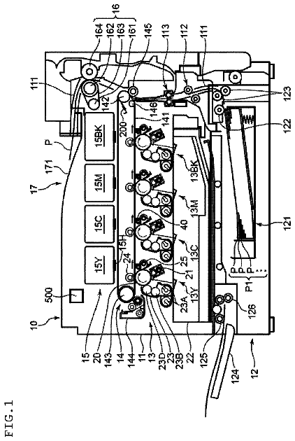
FIG. 1 illustrates the structure of an image forming apparatus according to an exemplary embodiment;
FIG. 2 illustrates the structure of an area around a photoconductor according to the exemplary embodiment;
FIG. 3 is a perspective view of a charging device according to the exemplary embodiment;
FIGS. 4A and 4B illustrate an attachment structure of the charging device according to the exemplary embodiment;
FIG. 5 is a plan view of a grid according to the exemplary embodiment;
FIG. 6 is a plan view of a grid according to the exemplary embodiment;
FIGS. 7A and 7B are enlarged partial plan views of the grid according to the exemplary embodiment;
FIGS. 8A and 8B are enlarged partial plan views of the grid according to the exemplary embodiment;
FIG. 9 is an enlarged partial plan view of a grid according to a first modification;
FIG. 10A is a plan view of a grid according to a second modification;
FIG. 10B is an enlarged partial plan view of the grid according to the second modification;
FIG. 11 is a plan view of a grid according to a third modification;
FIGS. 12A and 12B are enlarged partial plan views of the grid according to the third modification;
FIG. 13A is a plan view of a grid according to a fourth modification;
FIG. 13B is an enlarged partial plan view of the grid according to the fourth modification;
FIG. 14A is a plan view of a grid according to a fifth modification;
FIG. 14B is an enlarged partial plan view of the grid according to the fifth modification;
FIG. 15 is an enlarged partial plan view of a grid according to a sixth modification;
FIG. 16A is a plan view of a grid according to a seventh modification;
FIG. 16B is an enlarged partial plan view of the grid according to the seventh modification; and
FIG. 17 is a plan view of a grid according to an eighth modification.
An exemplary embodiment of the present invention will be described in detail with reference to the drawings.
Structure of Image Forming Apparatus of Exemplary Embodiment
First, the structure of an image forming apparatus according to the present exemplary embodiment will be described. FIG. 1 is a schematic diagram illustrating the structure of an image forming apparatus 10 according to the present exemplary embodiment.
The image forming apparatus 10 includes a sheet storing unit 12 in which sheets of recording paper 2, which are examples of recording media, are stored; an image forming unit 14 which is located above the sheet storing unit 12 and forms images on sheets of recording paper P fed from the sheet storing unit 12; and an original-document reading unit 16 which is located above the image forming unit 14 and reads an original document G. The image forming apparatus 10 also includes a controller 20 that is provided in the image forming unit 14 and controls the operation of each part of the image forming apparatus 10. In the following description, the vertical direction and the horizontal direction with respect to an apparatus body 10A of the image forming apparatus 10 will be referred to as the direction of arrow V and the direction of arrow H, respectively.
The sheet storing unit 12 includes a first storage unit 22, a second storage unit 24, and a third storage unit 26 in which sheets of recording paper P having different sizes are stored. Each of the first storage unit 22, the second storage unit 24, and the third storage unit 26 are provided with a feeding roller 32 that feeds the stored sheets of recording paper P to a transport path 28 in the image forming apparatus 10. Pairs of transport rollers 34 and 36 that transport the sheets of recording paper P one at a time are provided along the transport path 28 in an area on the downstream of each feeding roller 32. A pair of positioning rollers 38 are provided on the transport path 28 at a position downstream of the transport rollers 36 in a transporting direction of the sheets of recording paper P. The positioning rollers 38 temporarily stop each sheet of recording paper P and feed the sheet toward a second transfer position, which will be described below, at a predetermined timing.
In the front view of the image forming apparatus 10, an upstream part of the transport path 28 extends in the direction of arrow V from the left side of the sheet storing unit 12 to the lower left part of the image forming unit 14. A downstream part of the transport path 28 extends from the lower left part of the image forming unit 14 to a paper output unit 15 provided on the right side of the image forming unit 14. A duplex-printing transport path 29, which is provided for reversing and transporting each sheet of recording paper P in a duplex printing process, is connected to the transport path 28.
In the front view of the image forming apparatus 10, the duplex-printing transport path 29 includes a first switching member 31, a reversing unit 33, a transporting unit 37, and a second switching member 35. The first switching member 31 switches between the transport path 28 and the duplex-printing transport path 29. The reversing unit 33 extends linearly in the direction of arrow V from a lower right part of the image forming unit 14 along the right side of the sheet storing unit 12. The transporting unit 37 receives the trailing end of each sheet of recording paper P that has been transported to the reversing unit 33 and transports the sheet in the direction of arrow H. The second switching member 35 switches between the reversing unit 33 and the transporting unit 37. The reversing unit 33 includes plural pairs of transport rollers 42 that are arranged with intervals therebetween, and the transporting unit 37 includes plural pairs of transport rollers 44 that are arranged with intervals therebetween.
The first switching member 31 has the shape of a triangular prism, and a point end of the first switching member 31 is moved by a driving unit (not shown) to one of the transport path 28 and the duplex-printing transport path 29. Thus, the transporting direction of each sheet of recording paper P is changed. Similarly, the second switching member 35 has the shape of a triangular prism, and a point end of the second switching member 35 is moved by a driving unit (not shown) to one of the reversing unit 33 and the transporting unit 37. Thus, the transporting direction of each sheet of recording paper P is changed. The downstream end of the transporting unit 37 is connected to the transport path 28 by a guiding member (not shown) at a position in front of the transport rollers 36 in the upstream part of the transport path 28. A foldable manual sheet-feeding unit 46 is provided on the left side of the image forming unit 14. The sheets of recording paper P may be fed to the positioning rollers 38 on the transport path 28 from the manual sheet-feeding unit 46.
The original-document reading unit 16 includes a document transport device 52 that transports the sheets of the original document G one at a time; a platen glass 54 which is located below the document transport device 52 and on which the sheets of the original document G are placed one at a time; and an original-document reading device 56 that scans each sheet of the original document G while the sheet is being transported by the document transport device 52 or placed on the platen glass 54. The document transport device 52 includes a transport path 55 along which pairs of transport rollers 53 are arranged. A part of the transport path 55 is arranged such that each sheet of the original document G moves along the top surface of the platen glass 54. The original-document reading device 56 scans each sheet of the original document G that is being transported by the document transport device 52 while being stationary at the left edge of the platen glass 54. Alternatively, the original-document reading device 56 scans each sheet of the original document G placed on the platen glass 54 while moving in the direction of arrow H.
The image forming unit 14 includes a cylindrical or columnar photoconductor 62 as an example of a cylindrical or columnar member to be charged. The photoconductor 62 is arranged in a substantially central area of the apparatus body 10A. The photoconductor 62 is rotated in the direction shown by arrow +R (clockwise in FIG. 1) by a driving unit (not shown), and carries an electrostatic latent image formed by irradiation with light. In addition, a scorotron charging device 100 that charges the outer peripheral surface of the photoconductor 62 is provided above the photoconductor 62 so as to face the outer peripheral surface of the photoconductor 62. The detailed structure of the charging device 100 will be described below. The photoconductor 62 includes an overcoat layer that has high abrasion resistance but easily causes image degradation owing to discharge products generated by the charging device 100.
An exposure device 66 is provided so as to face the outer peripheral surface of the photoconductor 62 at a position downstream of the charging device 100 in the rotational direction of the photoconductor 62. The outer peripheral surface of the photoconductor 62 that has been charged by the charging device 100 is irradiated with light (exposed to light) by the exposure device 66 on the basis of an image signal corresponding to each color of toner. Thus, an electrostatic latent image is formed.
A rotation-switching developing device 70 is provided downstream of a position where the photoconductor 62 is irradiated with exposure light by the exposure device 66 in the rotational direction of the photoconductor 62. The developing device 70 visualizes the electrostatic latent image on the outer peripheral surface of the photoconductor 62 by developing the electrostatic latent image with toner of each color.
As illustrated in FIG. 2, the developing device 70 includes developing units 72Y, 72M, 72C, 72K, 72E, and 72F corresponding to the respective colors, which are yellow (Y), magenta (M), cyan (C), black (K), the first specific color (E), and the second specific color (F), respectively. The developing units 72Y, 72M, 72C, 72K, 72E, and 72F are arranged in that order in a circumferential direction (counterclockwise). The developing device 70 is rotated by a motor (not shown), which is an example of a rotating unit, in steps of 60.degree.. Accordingly, one of the developing units 72Y, 72M, 72C, 72K, 72E, and 72F that is to perform a developing process is selectively opposed to the outer peripheral surface of the photoconductor 62. The position at which each developing unit 72Y, 72M, 72C, 72K, 72E, and 72F is opposed to the outer peripheral surface of the photoconductor 62 is a developing position at which the developing process is performed. The developing units 72Y, 72M, 72C, 72K, 72E, and 72F have similar structures. Therefore, only the developing unit 72Y will be described, and explanations of the other developing units 72M, 72C, 72K, 72E, and 72F will be omitted.
The developing unit 72Y is filled with developer (not shown) including toner and carrier. The developer is supplied from a toner cartridge 78Y (see FIG. 1) through a toner supply channel (not shown). The developing unit 72Y is provided with a developing roller 74 having an outer peripheral surface that faces the outer peripheral surface of the photoconductor 62.
The developing roller 74 moves the developer layer on the outer peripheral surface of a developing sleeve 74A to the position where the developing sleeve 74A faces the photoconductor 62. Accordingly, the toner adheres to the latent image (electrostatic latent image) formed on the outer peripheral surface of the photoconductor 62. Thus, the latent image is developed.
Six developing rollers 74 are included in the respective developing units 72Y, 72M, 72C, 72K, 72E, and 72F, and are arranged along the circumferential direction so as to be separated from each other by 60.degree. in terms of the central angle. When the developing units 72Y, 72M, 72C, 72K, 72E, and 72F are switched, the developing roller 74 in the newly selected developing unit 72Y, 72M, 72C, 72K, 72E, and 72F is caused to face the outer peripheral surface of the photoconductor 62.
An intermediate transfer belt 68 is provided downstream of the developing device 70 in the rotational direction of the photoconductor 62 and below the photoconductor 62. A toner image formed on the outer peripheral surface of the photoconductor 62 is transferred onto the intermediate transfer belt 68. The intermediate transfer belt 68 is an endless belt, and is wound around a driving roller 61 that is rotated by the controller 20, a tension-applying roller 65 that applies a tension to the intermediate transfer belt 68, plural transport rollers 63 that are in contact with the back surface of the intermediate transfer belt 68 and are rotationally driven, and an auxiliary roller 69 that is in contact with the back surface of the intermediate transfer belt 68 at a second transfer position, which will be described below, and is rotationally driven. The intermediate transfer belt 68 is rotated in the direction shown by arrow -R (counterclockwise in FIG. 2) when the driving roller 61 is rotated.
A first transfer roller 67 is opposed to the photoconductor 62 with the intermediate transfer belt 68 interposed therebetween. The first transfer roller 67 performs a first transfer process in which the toner image formed on the outer peripheral surface of the photoconductor 62 is transferred onto the intermediate transfer belt 68. The first transfer roller 67 is in contact with the back surface of the intermediate transfer belt 68 at a position downstream of the position where the photoconductor 62 is in contact with the intermediate transfer belt 68 in the moving direction of the intermediate transfer belt 68. The first transfer roller 67 receives electricity from a power source (not shown), so that a potential difference is generated between the first transfer roller 67 and the photoconductor 62, which is grounded. Thus, the first transfer process is carried out in which the toner image on the photoconductor 62 is transferred onto the intermediate transfer belt 68.
A second transfer roller 71, which is an example of a transfer unit, is opposed to the auxiliary roller 69 with the intermediate transfer belt 68 interposed therebetween. The second transfer roller 71 performs a second transfer process in which toner images that have been transferred onto the intermediate transfer belt 68 in the first transfer process are transferred onto the sheet of recording paper P. The position between the second transfer roller 71 and the auxiliary roller 69 serves as the second transfer position at which the toner images are transferred onto the sheet of recording paper P. The second transfer roller 71 is in contact with the intermediate transfer belt 68. The second transfer roller 71 receives electricity from a power source (not shown), so that a potential difference is generated between the second transfer roller 71 and the auxiliary roller 69, which is grounded. Thus, the second transfer process is carried out in which the toner images on the intermediate transfer belt 68 are transferred onto the sheet of recording paper P.
A cleaning device 60, which is an example of a developer collecting device, is opposed to the driving roller 61 with the intermediate transfer belt 68 interposed therebetween. The cleaning device 60 collects residual toner that remains on the intermediate transfer belt 68 after the second transfer process. The cleaning device 60 includes a cleaning blade 64 that comes into contact with the intermediate transfer belt 68 to remove the toner from the intermediate transfer belt 68. The cleaning blade 64 of the cleaning device 60 and the second transfer roller 71 are separated from the outer peripheral surface of the intermediate transfer belt 68 until the toner images of the respective colors are transferred onto the intermediate transfer belt 68 in a superimposed manner (first transfer process) and then transferred onto the sheet of recording paper P (second transfer process).
A position detection sensor 83 is opposed to the tension-applying roller 65 at a position outside the intermediate transfer belt 68. The position detection sensor 83 detects a predetermined reference position on the surface of the intermediate transfer belt 68 by detecting a mark (not shown) on the intermediate transfer belt 68. The position detection sensor 83 outputs a position detection signal that serves as a reference for the time to start an image forming process.
A cleaning device 73 is provided downstream of the first transfer roller 67 in the rotational direction of the photoconductor 62. The cleaning device 73 removes residual toner and the like that remain on the surface of the photoconductor 62 instead of being transferred onto the intermediate transfer belt 68 in the first transfer process. The cleaning device 73 collects the residual toner and the like with a cleaning blade and a brush roller that are in contact with the surface of the photoconductor 62. An erase device 81 is provided upstream of the cleaning device 73 and downstream of the first transfer roller 67 in the rotational direction of the photoconductor 62. The erase device 81 eliminates the charge history left by the first transfer roller 67 by discharging electricity toward the outer peripheral surface of the photoconductor 62. The erase device 81 discharges negative electricity toward the outer peripheral surface of the photoconductor 62 before the residual toner and the like are collected by the cleaning device 73. Accordingly, the history of positive electric charge left by the first transfer roller 67 is eliminated, and the image forming process of the next cycle is prevented from being affected by the electric charge. An erase unit 75 that irradiates the outer peripheral surface of the photoconductor 62 with light to eliminate the history of the negative electric charge is provided downstream of the cleaning device 73 and upstream of the charging device 100.
As illustrated in FIG. 1, the second transfer position at which the toner images are transferred onto the sheet of recording paper P by the second transfer roller 71 is at an intermediate position of the above-described transport path 28. A fixing device 80 is provided on the transport path 28 at a position downstream of the second transfer roller 71 in the transporting direction of the sheet of recording paper P (direction shown by arrow A). The fixing device 80 fixes the toner images that have been transferred onto the sheet of recording paper P by the second transfer roller 71. The fixing device 80 includes a heating roller 82 and a pressing roller 84. The heating roller 82 is disposed at the side of the sheet of recording paper P at which the toner images are formed (upper side), and includes a heat source which generates heat when electricity is supplied thereto. The pressing roller 84 is positioned below the heating roller 82, and presses the sheet of recording paper P against the outer peripheral surface of the heating roller 82. Transport rollers 39 that transport the sheet of recording paper P to the paper output unit 15 or the reversing unit 33 are provided on the transport path 28 at a position downstream of the fixing device 80 in the transporting direction of the sheet of recording paper P.
Toner cartridges 78Y, 78M, 78C, 78K, 78E, and 78F that respectively contain yellow (Y) toner, magenta (M) toner, cyan (C) toner, black (K) toner, toner of a first specific color (E), and toner of a second specific color (F) are arranged in the horizontal direction in a replaceable manner in an area below the original-document reading device 56 and above the developing device 70. The first and second specific colors E and F may be selected from specific colors (including transparent) other than yellow, magenta, cyan, and black. Alternatively, the first and second specific colors E and F are not selected. When the first and second specific colors E and F are selected, the developing device 70 performs the image forming process using six colors, which are Y, M, C, K, F, and F. When the first and second specific colors E and F are not selected, the developing device 70 performs the image forming process using four colors, which are Y, M, C, and K. In the present exemplary embodiment, the case in which the image forming process is performed using the six colors, which are Y, M, C, K, F, and F will be described as an example. However, as another example, the image forming process may be performed using five colors, which are Y, M, C, K, and one of the first and second specific colors E and F.
Structure of Charging Device 100
The structure of the charging device 100 will now be described.
As illustrated in FIG. 2, the charging device 100 includes a shield case 102 made of aluminum as an example of a housing that is open at the side opposed to the photoconductor 62. The shield case 102 has the shape of a long box (see FIG. 3) that extends in an axial direction of the photoconductor 62. As illustrated in FIG. 2, a partition plate 104 is provided in the shield case 102 so as to divide the inner space of the shield case 102 at a central position thereof in the width direction (circumferential direction of the photoconductor 62).
Discharge wires 106 and 108, which are examples of discharge electrodes, are arranged in the shield case 102 at either side of the partition plate 104. The discharge wires 106 and 108 extend in the axial direction of the photoconductor 62. The discharge wires 106 and 108 are formed of metal wires made of tungsten or the like. The discharge electrodes may instead be discharge members formed of wires coated with resin or metal plates, and are not limited as long as the discharge electrodes are capable of discharging electricity.
The discharge wires 106 and 108 generate a negative charge when a voltage is applied thereto from a power source (not shown), and performs a discharging operation of supplying the negative charge to the surface of the photoconductor 62. The photoconductor 62 is charged with electricity as a result of this discharging operation.
A grid 110, which is an example of a potential control plate, is disposed between the photoconductor 62 and the discharge wires 106 and 108 at the open side of the shield case 102. The grid 110 extends along the axial direction of the photoconductor 62.
The grid 110 extends in the axial direction of the photoconductor 62. In other words, the long-side direction of the grid 110 extends along the axial direction of the photoconductor 62, and the short-side direction of the grid 110 extends along the circumferential direction of the photoconductor 62. The grid 110 is formed of a metal plate in which plural openings 119 are formed (see, for example, FIGS. 7A and 7B). The openings 119 are formed as spaces obtained by sectioning slits 128 between structural lines 127 to 129 and 130, which will be described below, with beams 140, which will be described below.
The negative charge generated by the discharge wires 106 and 108 is supplied to the photoconductor 62 through the openings 119 formed in the grid 110. The amount of negative charge that passes through the grid 110 is controlled by a grid voltage, which is controlled by a controller (not shown). Thus, the charge potential of the photoconductor 62 is controlled.
More specifically, in the case where the voltage (potential) of the grid 110 is higher than the potential of the photoconductor 62, the negative charge moves toward the photoconductor 62 due to the potential difference between the photoconductor 62 and the grid 110. Accordingly, a large amount of negative charge passes through the grid 110. When the negative charge is supplied to the photoconductor 62, the potential difference between the photoconductor 62 and the grid 110 decreases. Accordingly, the amount of negative charge that passes through the grid 110 decreases. Thus, when the grid voltage of the grid 110 is high, compared to the case in which the grid voltage is low, the amount of negative charge that passes through the grid 110 is increased and the charge potential of the photoconductor 62 is increased accordingly.
As illustrated in FIG. 3, the charging device 100 includes a cleaning member 126 that cleans the discharge wires 106 and 108 and the grid 110 by moving along the axial direction of the photoconductor 62 while being in contact with the discharge wires 106 and 108 and the grid 110. The cleaning member 126 includes portions that sandwich the grid 110 from both sides thereof in the thickness direction. The cleaning member 126 may be formed of, for example, a porous material, such as sponge, or a brush-shaped cleaning brush.
Attachment Structure of Grid 110
As illustrated in FIG. 3, the charging device 100 includes attachment members 112 and 114, which are examples of curve regulating members, at both ends of the shield case 102 in the long-side direction thereof. The attachment members 112 and 114 are used to attach (retain) the grid 110. The attachment member 112 is provided at one end (lower left end in FIG. 3) of the shield case 102 in the long-side direction, and the attachment member 114 is provided at the other end (upper right end in FIG. 3) of the shield case 102 in the long-side direction. In FIG. 3, the direction shown by arrow D is the long-side direction of the grid 110, the direction shown by arrow S is the short-side direction of the grid 110, and the direction shown by arrow T is the thickness direction of the grid 110. The directions shown by arrows D, S, and T are orthogonal to each other.
As illustrated in FIG. 5, the grid 110 has the shape of a plate (a rectangular shape in plan view and a plate shape in side view) that has a long-side direction in the axial direction of the photoconductor 62 (see FIG. 2) (direction shown by arrow D) when no load is applied. The grid 110 is elastically deformed and curved when a load is applied thereto. The grid 110 includes an attachment portion 104A having a width W1, an electrode portion 104B having a width W2, and an attachment portion 104C having a width W3, which are arranged along the long-side direction of the grid 110 and integrated with each other.
The grid 110 is retained in a tensioned state at both ends thereof in the long-side direction, and a voltage is applied to the grid 110 by a feeder unit (not shown). Here, members having the shape of a plate are not limited to flat plate-shaped members, and include members that are slightly curved when viewed in the direction shown by arrow D.
The attachment portion 104A has attachment holes 116A and 116B, which are through holes that extend through the attachment portion 104A in the thickness direction of the grid 110. The attachment holes 116A and 116B have a rectangular shape and are formed with an interval therebetween in the short-side direction of the grid 110 (direction shown by arrow S).
An attachment piece 118 that projects outward in the long-side direction of the grid 110 is formed on the attachment portion 104C. The attachment piece 118 includes two support portions 118A that are slanted toward each other in plan view and a hook portion 118B that is angular-U-shaped in plan view and that is integrated with each of the two support portions 118A at an end thereof (at the right end in FIG. 5). The other end (the left end in FIG. 5) of each support portion 118A is integrated with a surface 104D at an end of the grid 110 (right end face in FIG. 5) at a central area thereof in the direction shown by arrow S.
Referring to FIG. 4A, the attachment member 112 includes a curved surface 112A and side surfaces 112C. The curved surface 112A is disposed between the grid 110 and the discharge wires 106 and 108 (see FIG. 2) and extends along the outer peripheral surface of the photoconductor 62 (see FIG. 2). The side surfaces 112C extend in the direction shown by arrow T from the ends of the curved surface 112A in the direction shown by arrow S.
Two L-shaped hook portions 112E that project toward the photoconductor 62 (upward in FIG. 4A) and that are bent outward in the axial direction of the photoconductor 62 (toward the upper left in FIG. 4A) are formed on the curved surface 112A. The size of the two hook portions 112B is set such that the hook portions 112B may be inserted into the attachment holes 116A and 116B. The hook portions 112B are formed of leaf springs and pull the grid 110 outward in the axial direction of the photoconductor 62 (toward the upper left in FIG. 4A). Thus, the hook portions 112B serve as tension applying members that apply a tension to the grid 110 in the axial direction of the photoconductor 62.
Projections 1120 used to fix a leaf spring 122, which will be described below, project from the side surfaces 112C of the attachment member 112 (only one of the side surfaces 112C is illustrated). The hook portions 112B are engaged with the edges of the attachment holes 116A and 116B in the grid 110, so that a first end of the grid 110 is positioned. The grid 110 is retained at the first end thereof by the urging force applied by the leaf spring 122, which is an example of a curve maintaining member, such that the grid 110 is curved along the outer peripheral surface of the photoconductor 62.
The leaf spring 122 includes a curved portion 122A and attachment portions 122B which are integrated with each other. The curved portion 122A extends in the direction shown by arrow S and is curved to be convex in the direction shown by arrow T (downward in FIG. 4A). The attachment portions 122B extend in the direction shown by arrow T from the ends of the curved portion 122A in the direction shown by arrow S. Engagement holes 122C, with which the projections 112D are engaged, are formed in the attachment portions 122B. The convex surface of the curved portion 122A serves as a contact surface 122D that contacts the grid 110.
Referring to FIG. 4B, the attachment member 114 includes a curved surface 114A, side surfaces 114B, and an attachment surface 114C. The curved surface 114A is disposed between the grid 110 and the discharge wires 106 and 108 (see FIG. 2) and extends along the outer peripheral surface of the photoconductor 62 (see FIG. 2). The side surfaces 114B extend in the direction shown by arrow T from the ends of the curved surface 114A in the direction shown by arrow S. The attachment surface 114C is provided at the second end in the direction shown by arrow D such that the attachment surface 114C is lower than the curved surface 114A.
An L-shaped hook portion 114D that projects toward the photoconductor 62 (upward in FIG. 4B) and that is bent outward in the axial direction of the photoconductor 62 (toward the lower right in FIG. 4B) are formed on the attachment surface 114C. The hook portion 114D is formed on the attachment surface 1140 at a central area thereof in the direction shown by arrow S. The size of the hook portion 114D is set such that the hook portion 118B of the grid 110 may be engaged with the hook portion 114D. The hook portion 114D is formed of a leaf spring and pulls the grid 110 outward in the axial direction of the photoconductor 62 (toward the lower right in FIG. 4B). Thus, the hook portion 114D serves as a tension applying member that applies a tension to the grid 110 in the axial direction of the photoconductor 62.
Projections 114E used to fix a leaf spring 124, which will be described below, project from the side surfaces 114B of the attachment member 114 (only one of the side surfaces 114B is illustrated). The hook portion 118B of the grid 110 is engaged with the hook portion 114D, so that a second end of the grid 110 is positioned. The grid 110 is retained at the second end thereof by the urging force applied by the leaf spring 124, which is an example of a curve maintaining member. Accordingly, the state in which the grid 110 is curved along the outer peripheral surface of the photoconductor 62 is maintained.
The leaf spring 124 includes a curved portion 124A and attachment portions 124B which are integrated with each other. The curved portion 124A extends in the direction shown by arrow S and is curved to be convex in the direction shown by arrow T (downward in FIG. 4B). The attachment portions 124B extend in the direction shown by arrow T from the ends of the curved portion 124A in the direction shown by arrow S. Engagement holes 124C, with which the projections 114E are engaged, are formed in the attachment portions 124B. The convex surface of the curved portion 124A serves as a contact surface 1240 that contacts the grid 110.
Projecting contact portions (not shown) formed on the leaf springs 122 and 124 are in contact with top portions of holders (not shown) provided at the ends of the photoconductor 62 (see FIG. 2), so that a distance between the photoconductor 62 and the grid 110 is maintained at a certain distance.
The hook portions 112B and 114D may pull the grid 110 toward the discharge wires 106 and 108 (downward in FIGS. 4A and 4B) so as to curve the grid 110 by urging the grid 110 against the curved surfaces 112A and 114A. In such a case, the leaf springs 122 and 124, which are examples of curve maintaining members, may be omitted.
Structure of Electrode Portion 104B of Grid 110
The structure of the electrode portion 104B of the grid 110 will now be described. FIGS. 6 to 85 illustrate the structure of the electrode portion 104B of the grid 110. In FIGS. 3 to 5, thin lines 130, which will be described below, are not illustrated.
As illustrated in FIGS. 6 and 7A, the electrode portion 104B of the grid 110 includes plural (at least three) thin lines 130. The thin lines 130 are arranged along the circumferential direction of the photoconductor 62 (direction shown by arrow S) and linearly extend along the axial direction of the photoconductor 62 (direction shown by arrow D). Linear portions 127 and 129 are provided at both ends of the grid 110 in the short-side direction thereof (in the direction shown by arrow S). The linear portions 127 and 129 linearly extend along the axial direction of the photoconductor 62 with all of the thin lines 130 disposed therebetween. In the present exemplary embodiment, the linear portions 127 and 129 and the thin lines 130 serve as structural lines that linearly extend in the axial direction of the photoconductor 62. In the following description, the linear portions 127 and 129 and the thin lines 130 are sometimes referred to as structural lines 127 to 129 and 130.
Each of the linear portions 127 and 129 and the thin lines 130 is fixed to the attachment portion 104A at one end thereof and to the attachment portion 104C at the other end thereof. Thus, the thin lines 130 are surrounded by a frame-shaped structure including the linear portions 127 and 129 and the attachment portions 104A and 104C.
As illustrated in FIG. 7A, the electrode portion 104B of the grid 110 includes plural beams 140, which are examples of connecting portions that connect two or more of the structural lines 127 to 129 and 130 that are next to each other in the circumferential direction of the photoconductor 62 (direction shown by arrow S). More specifically, each beam 140 connects two of the structural lines 127 to 129 and 130 that are next to each other in the circumferential direction of the photoconductor 62.
The plural beams 140 are arranged in the axial direction of the photoconductor 62 (direction shown by arrow D). According to the present exemplary embodiment, the structure in which the beams 140 are arranged in the axial direction of the photoconductor 62 is the structure in which one of the beams 140 and another one of the beams 140 are disposed at different positions in the axial direction of the photoconductor 62. Therefore, the structure in which the beams 140 are arranged in the axial direction of the photoconductor 62 includes the structure in which the beams 140 are arranged in the axial direction of the photoconductor 62 while positions thereof in the circumferential direction of the photoconductor 62 are shifted from each other.
In the present exemplary embodiment, the beams 140 in the electrode portion 104B are formed such that plural beam groups 150 which each include plural beams 140 are provided. In each beam group 150, the beams 140 are continuously arranged in the axial direction of the photoconductor 62 from the linear portion 127 to the linear portion 129. As illustrated in FIG. 6, the beam groups 150 include two sets of beam groups 150A, 150B, 150C, and 150D, and eight beam groups in total are provided. The beam groups are arranged in order of 150A, 1508, 150C, 150D, 150A, 150B, 150C, and 150D, along the axial direction of the photoconductor 62. Each of the beam groups 150A, 1508, 150C, and 150D includes, for example, ten beams 140. In FIG. 6, the beam groups 150A, 150B, 150C, and 150D are drawn in a simplified manner.
In each of the beam groups 150A, 150B, 150C, and 150D, the beams 140 are arranged at a constant pitch along the circumferential direction of the photoconductor 62. In other words, the beams 140 are arranged with the same number of slits 128 (the same number of thin lines 130) disposed therebetween. In the present exemplary embodiment, the beams 140 are arranged with three slits 128 and two thin lines 130 disposed therebetween.
More specifically, in each of the two beam groups 150A, the first beam 140A from the bottom in FIG. 7A connects the first and second thin lines 130 from the bottom in FIG. 7A to each other. The second beam 1408 skips three slits 128 and connects the fifth and sixth thin lines 130 to each other. The third beam 140C skips three slits 128 and connects the ninth and tenth thin lines 130 to each other. In this manner, the beams 140 connect two thin lines 130 to each other at positions where three slits 128 are disposed between the beams 140. In FIG. 7A, only the beam group 150A near the attachment portion 104C is illustrated.
The description continues in the full USPTO document.
About 6,828 words. The USPTO PDF has it with every drawing.
Fees are due 3.5, 7.5 and 11.5 years after grant. This patent expired on June 10, 2026, so the fee marked "not paid" was the one that went unpaid.
CHARGING DEVICE, IMAGE FORMING APPARATUS, AND POTENTIAL CONTROL PLATE
Filed Sep 2011 · published Oct 2012Charging device, image forming apparatus, and potential control plate
Filed Sep 2011 · granted Jun 2014Earlier publications, parents and continuations. None of them can still be enforced, or this patent would not be listed.
Prior art cited by the examiner or applicant. Useful when you check your own idea for novelty.
Everything on this page comes from the documents linked above.


