 Lapsed, fee not paid11 drawings
Hardware & Electronics · US 8,743,012 B2
Broad-band, multi-band antenna
A broad-band, multi-band antenna.
US 8,743,014 B2 · Assignee: Sharp Kabushiki Kaisha · Inventors: Kondo; Toshinori et al.
Sheet 1 of 29 from the published document. All sheets in the USPTO PDF
At least three resonance frequencies are obtained by two antenna elements. The antenna device includes antenna elements (11) and (12), a wireless section (20) for supplying power to each of the antenna elements (11) and (12), a PIN diode (16) for electrically connecting and disconnecting the antenna element (11) and the wireless section (20) with/from each other, the antenna elements (11) and (12) being provided so as to be capacitively coupled to each other during the electrical disconnection between the antenna element (11) and the wireless section (20) which electrical disconnection is made by the PIN diode (16).
Generally, in order to obtain resonance at different frequencies in an antenna device, it is only necessary to provide the antenna device with antenna elements as many as the number of the different frequencies and a transmitting/receiving circuit for causing the antenna elements to operate. However, it is necessary to secure a large space in an antenna device so as to provide an additional antenna element and a transmitting/receiving circuit. Namely, as the number of frequencies at which resonance occurs increases in an antenna device, the antenna device becomes larger. In view of the circumstances, ways and means to miniaturize an antenna device while obtaining resonance at different frequencies have been suggested. For example, Patent Literature 1 discloses an antenna device which causes a switch to connect/disconnect two antenna elements with/from each other. According to the antenna
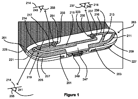
1 of 29 drawing sheets so far from the published document, cropped to the drawing. Every sheet is in the USPTO PDF.
What the patent claimed, word for word. All of it is now free to use.
The present invention relates to an antenna device and a wireless communication terminal each of which is capable of changing a resonance frequency.
Generally, in order to obtain resonance at different frequencies in an antenna device, it is only necessary to provide the antenna device with antenna elements as many as the number of the different frequencies and a transmitting/receiving circuit for causing the antenna elements to operate. However, it is necessary to secure a large space in an antenna device so as to provide an additional antenna element and a transmitting/receiving circuit. Namely, as the number of frequencies at which resonance occurs increases in an antenna device, the antenna device becomes larger.
In view of the circumstances, ways and means to miniaturize an antenna device while obtaining resonance at different frequencies have been suggested.
For example, Patent Literature 1 discloses an antenna device which causes a switch to connect/disconnect two antenna elements with/from each other.
According to the antenna device disclosed in Patent Literature 1, a change made by the switch causes the antenna device to resonate with signals of two kinds of frequencies by changing a substantial length (hereinafter referred to as an electrical length) of an antenna operating as an antenna, so as to miniaturize the antenna device by causing circuits required to be provided for respective antenna elements to be shared.
Patent Literature 1 Japanese Patent Application Publication, Tokukai, No. 2008-29001 A (Publication Date: Feb. 7, 2008)
Technical Problem
However, according to the prior art as described above, only at most two kinds of resonance frequencies can be obtained by two antenna elements since electrical lengths of two antenna elements are changed merely by electrically connecting and disconnecting the two antenna elements with/from each other.
The present invention has been made in view of the problems, and an object of the present invention is to provide an antenna device which is capable of obtaining at least three resonance frequencies by two antenna elements, and a wireless communication terminal.
Solution to Problem
In order to attain the object, an antenna device according to the present invention includes: a first antenna element; a second antenna element; a power supply section for supplying power to each of the first antenna element and the second antenna element; and a switching element for electrically connecting and disconnecting the first antenna element and the power supply section with/from each other, the first antenna element and the second antenna element being provided so as to be capacitively coupled to each other during the electrical disconnection between the first antenna element and the power supply section which electrical disconnection is made by the switching element.
According to the arrangement, each of the first antenna element and the second antenna element operates as a 1/4 wavelength antenna at a corresponding specified resonance frequency in response to a power supply from the power supply section during the electrical connection between the first antenna element and the power supply section which electrical connection is made by the switching element in a first power supply path.
In contrast, the first antenna element and the second antenna element are in a state in which a charge exchange occurs therebetween, i.e., they are capacitively coupled (hereinafter referred to as "electrically coupled") during the electrical disconnection between the first antenna element and the power supply section which electrical disconnection is made by the switching element in the first power supply path.
This allows the first antenna element to receive power from the power supply section via the second antenna element.
In this case, the first antenna element operates as a 1/2 wavelength antenna since both ends of the first antenna element are open. Accordingly, the first antenna element resonates at a higher resonance frequency than in the case of the electrical connection between the first antenna element and the power supply section.
Namely, it is possible to change operation as an antenna of the first antenna element by causing the switching element to electrically connect/disconnect the first antenna element and the power supply section with/from each other.
The second antenna element, which operates as a 1/4 wavelength antenna in response to a power supply from the power supply section even during the electrical disconnection between the first antenna element and the power supply section which disconnection is made by the switching element, has a longer electrical length by being electrically connected to the first antenna element due to the capacitive coupling. According to this, the second antenna element resonates at a lower frequency than in the case of the electrical connection between the first antenna element and the power supply section.
As a result, it is possible to cause the first antenna element and the second antenna element to operate at different frequencies, depending on whether the first antenna element and the power supply section are electrically connected or disconnected with/from each other.
Namely, it is possible to obtain at least three resonance frequencies by the first antenna element and the second antenna element.
Advantageous Effects of Invention
An antenna device according to the present invention includes: a first antenna element; a second antenna element; a power supply section for supplying power to each of the first antenna element and the second antenna element; and a switching element for electrically connecting and disconnecting the first antenna element and the power supply section with/from each other, the first antenna element and the second antenna element being provided so as to be capacitively coupled to each other during the electrical disconnection between the first antenna element and the power supply section which electrical disconnection is made by the switching element.
This brings about an effect of obtaining at least three resonance frequencies by two antenna elements.
For a fuller understanding of the nature and advantages of the invention, reference should be made to the ensuing detailed description taken in conjunction with the accompanying drawings.
FIG. 1, which illustrates how members are arranged in an antenna device according to an embodiment of the present invention, is a perspective view in which the antenna device is seen from one direction.
FIG. 2 has perspective views respectively illustrating mobile phones for each of which the antenna device according to the embodiment of the present invention is to be provided. (a) of FIG. 2 illustrates an appearance of the mobile phone, and (b) of FIG. 2 illustrates an antenna device and the like which are contained in a housing (not illustrated) of the mobile phone.
FIG. 3 is a functional block diagram schematically illustrating an arrangement of a mobile phone.
FIG. 4 is a schematic view schematically illustrating a circuit configuration of an antenna control section according to the embodiment of the present invention.
FIG. 5 is a circuit diagram illustrating a circuit configuration of a diode control circuit.
FIG. 6 is a graph schematically illustrating a return loss characteristic of the antenna device according to the embodiment of the present invention.
FIG. 7, which is a perspective view in which the antenna device according to the embodiment of the present invention is seen from another direction, illustrates an example of the antenna device.
FIG. 8 is a circuit diagram illustrating an example of a circuit configuration of a matching circuit.
FIG. 9 is a graph illustrating a return loss characteristic of the antenna device according to Example 1.
FIG. 10 is a graph illustrating a return loss characteristic of the antenna device according to Example 2.
FIG. 11 is a graph illustrating a return loss characteristic of the antenna device according to Example 3.
FIG. 12 is a graph illustrating a return loss characteristic of the antenna device according to Example 4.
FIG. 13 is a graph illustrating a return loss characteristic of the antenna device according to Example 5.
FIG. 14 is a graph illustrating a return loss characteristic of the antenna device according to Example 6.
FIG. 15, which is a perspective view in which the antenna device according to the embodiment of the present invention is seen from a first direction, illustrates a consideration example of the antenna device.
FIG. 16, which is a perspective view in which the antenna device according to the embodiment of the present invention is seen from a second direction, illustrates a consideration example of the antenna device.
FIG. 17 is a graph illustrating a return loss characteristic of the antenna device according to Consideration Example 1.
FIG. 18, which is a perspective view in which the antenna device according to the embodiment of the present invention is seen from one direction, illustrates a consideration example of the antenna device.
FIG. 19 is a flowchart illustrating how resonance frequencies are changed in the antenna device.
FIG. 20 is a perspective view illustrating another example of the antenna device according to the embodiment of the present invention.
FIG. 21 is a circuit diagram illustrating an example of the circuit configuration of the matching circuit.
FIG. 22 is a graph illustrating a return loss characteristic of the antenna device according to Example 7.
FIG. 23 is a perspective view illustrating a further example of the antenna device according to the embodiment of the present invention.
FIG. 24 is a circuit diagram illustrating an example of the circuit configuration of the matching circuit.
FIG. 25 is a graph illustrating a return loss characteristic of the antenna device according to Example 8.
FIG. 26 is a circuit diagram illustrating a modification of the circuit configuration of the diode control circuit.
FIG. 27 is a schematic view schematically illustrating a circuit configuration of the antenna device.
FIG. 28 is a circuit diagram illustrating a circuit configuration of a matching circuit according to another embodiment of the present invention.
FIG. 29 is a graph illustrating a return loss characteristic of an antenna device according to another embodiment of the present invention.
First Embodiment
An embodiment of an antenna device of the present invention is described below with reference to FIGS. 1 through 26.
First, a mobile phone (wireless communication terminal) provided with an antenna device according to the present embodiment is to be described with reference to FIG. 2. FIG. 2 has perspective views respectively illustrating typical examples of a mobile phone for which the antenna device according to the present embodiment is to be provided. (a) of FIG. 2 illustrates an appearance of the mobile phone, and (b) of FIG. 2 illustrates an antenna device and the like which are contained in a housing (not illustrated) of the mobile phone.
(Appearance of Mobile Phone)
A mobile phone 1 provided with an antenna device 50 typically includes a housing 3 including a display section 54 and an operation section 57 (see (a) of FIG. 2). The display 54 carries out display for providing various pieces of information for a user. The operation section 57 receives operation carried out by the user. The mobile phone 1 can be connected to a communication system such as a mobile phone network in response to the operation received by the control section 57.
A circuit board 2 for variously controlling the mobile phone 1 is provided in the housing 3 of the mobile phone 1 (see (b) of FIG. 2). The circuit board 2 includes an antenna control section 8 for controlling an antenna. The antenna device 50 includes (i) the circuit board 2 including the antenna control section 8 and (ii) an antenna section 10.
Note that the housing 3 of the mobile phone 1 can be foldably or slidably structured, i.e., can have any structure.
(Various Functions of Mobile Phone)
Next, various functions of the mobile phone 1 is to be described with reference to FIG. 3. FIG. 3 is a functional block diagram schematically illustrating an arrangement of a mobile phone.
The mobile phone 1 includes a control section 19, a vibration section 51, an illumination section 52, a storage section 53, the display section 54, an audio output section 55, an audio input section 56, the operation section 57, a wireless section (power supply section) 20, a switch section 58, and the antenna section 10 (see FIG. 3).
The control section 19 comprehensively controls various members of the mobile phone 1. A function of the control section 19 can be realized by, for example, causing a CPU (Central Processing Unit) to carry out a program stored in a storage element such as a RAM (Random Access Memory) or a flash memory. According to the present embodiment, the control section 19 particularly includes a communication control section 59 for controlling the switch section 58 and the wireless section 20.
The vibration section 51 causes a vibration element such as an eccentric motor to vibrate the mobile phone 1, so as to let the user know that a phone call has been received.
The illumination section 52 causes a light-emitting element such as an LED (a light emitting diode) to carry out light irradiation.
The storage section 53 stores various data and programs. The storage section 53 can be constituted by a flash memory, a ROM, a RAM, or the like.
The display section 54 receives image data from the control section 19 and displays an image on a display screen in accordance with the received image data. Specifically, an LCD (a Liquid Crystal Display) and an organic EL (Electro Luminescence) display, or the like is usable as the display section 54.
The audio output section 55 converts, to a sound wave, an audio signal supplied from the control section 19, so as to output the sound wave to outside. Specifically, the audio output section 55 includes a receiver, a speaker, a connector for audio output. For example, the mobile phone 1 is arranged such that the receiver is used for making a phone call and the speaker is used for letting the user know that a phone call has been received. Further, it is possible to connect the connector for audio output of the audio output section 55 to a headset, via which an audio is outputted.
The audio input section 56 converts an audio wave received from outside to an audio signal which is an electric signal, so as to transmit the audio signal to the control section 19. Specifically, the audio input section 56 includes a microphone.
The operation section 57 prepares operation data in response to operation carried out by the user with respect to an input device such as an operation button provided on a surface of the housing 3 included in the mobile phone 1, so as to transmit the operation data to the control section 19. A touch panel or the like other than a button switch is usable as the input device.
The wireless section 20 modulates, to a transmitted signal, transmitted data received from the control section 19, so as to transmit the modulated transmitted signal to outside via the antenna section 10. Further, the wireless section 20 demodulates, to received data, a received signal received from outside via the antenna section 10, so as to transmit the demodulated received data to the control section 19. Note that a circuit inside the wireless section 20 is selected by a filter or changed by a switch in accordance with a system (frequency band) to be used, so that the mobile phone 1 can be used in each communication system.
The switch section 58 changes a resonance frequency of the antenna section 10 in response to the control by the control section 19.
The antenna section 10 sends/receives a radio wave to/from outside.
Note that the antenna control section 8 illustrated in (b) of FIG. 2 corresponds to three functional blocks of the wireless section 20, the switch section 58, and the communication control section 59.
(Members of Antenna Device)
Subsequently, members of the antenna device 50 are to be described with reference to FIG. 1. FIG. 1, which illustrates how the members are arranged in the antenna device 50 according to the present embodiment, is a perspective view in which the antenna device 50 is seen from one direction.
Note that, for convenience, a direction of an arrow P1 is defined as "an upward direction". Note also that, in the drawings subsequent to FIG. 1, members having functions identical to those of the respective members illustrated in FIG. 1 are given respective identical reference numerals, and a description of those members is omitted there, unless otherwise noted.
First, how the members of the antenna device 50 are arranged is to be described with reference to FIG. 1. The antenna device 50 includes the antenna section 10 and the circuit board 2 (see FIG. 1).
The antenna section 10 includes an antenna base 9 and antenna elements (a first antenna element and a second antenna element) 11 and 12.
The antenna base 9 made of a dielectric material is provided on an end of the circuit board 2, and the antenna elements 11 and 12 for transmitting/receiving a radio wave are provided on a surface of the antenna base 9 (see FIG. 1).
The circuit board 2 is a board which includes the antenna control section 8 for controlling the antenna section 10. Note that the circuit board 2 can be provided with a circuit for realizing the various functions of the mobile phone 1.
The antenna control section 8 includes antenna connecting sections (connecting parts) 41 and 42 serving as plate spring terminals for connecting the antenna control section 8 to the respective antenna elements 11 and 12.
The antenna elements 11 and 12 are made of a plate electroconductive member. Lines of the respective antenna elements 11 and 12 extend upward along a side surface of the antenna base 9 from connecting parts of the lines and the respective antenna connecting sections 41 and 42 and then reach a top surface of the antenna base 9, on which the lines respectively extend while being bent. Note that examples of a shape, a length, a width, the number of bends, and the like of the antenna, each of which can be appropriately changed, are to be specifically described later.
Assuming that a resonance frequency of the antenna element 11 is denoted as f and a wavelength to f is denoted as .lamda., a distance W11 between the antenna connecting sections 41 and 42 is less than .lamda./15 which is one-fifteenth of .lamda. where an electrical length of the antenna element 11 is .lamda./4.
For example, the present embodiment is arranged such that the antenna element 11 has a longer line length than the antenna element 12. According to this, the antenna element 11 has a longer electrical length than the antenna element 12.
(Circuit Configuration of Antenna Control Section)
Next, a circuit configuration of the antenna control section 8 is to be described with reference to FIG. 4. FIG. 4 is a schematic view schematically illustrating the circuit configuration of the antenna control section 8.
The antenna control section 8 includes a power supply line 13, a matching circuit (an impedance matching circuit) 14, power supply connecting sections (the first power supply path and the second power supply path) 15a and 15b, a PIN diode (a switching element or a semiconductor element) 16, a diode control circuit 17, a signal line 18, the control section 19, the wireless section (power supply section) 20, a choke coil 21, a DC cut 22, and the antenna connecting sections 41 and 42.
The antenna element 11 is connected to the antenna connecting section 41 in the antenna control section 8 (see FIG. 4). The antenna connecting section 41 is connected to the power supply connecting section 15a.
The power supply line 13 has (i) one end to which the power supply connecting section 15a is connected via the DC cut 22 and the matching circuit 14 and (ii) the other end which is connected to the wireless section 20 so as to transmit, to the antenna element 11, a high-frequency current supplied from the wireless section 20. Note that the DC cut 22, which is provided so as to prevent a direct current from entering the wireless section 20 and transmissively supplies a high-frequency current, has no influence on a high-frequency characteristic of the antenna control section 8.
The PIN diode 16 is provided between the antenna connecting section 41 and the DC cut 22. A control voltage supplied from the diode control circuit 17 which is connected between the antenna connecting section 41 and the PIN diode 16 changes on/off states of the PIN diode 16.
The antenna element 12 is connected to the antenna connecting section 42. The antenna connecting section 42 is connected to the power supply connecting section 15b.
The power supply connecting section 15b is connected to the power supply line 13 via the DC cut 22 and the matching circuit 14. The choke coil 21 is connected to the power supply connecting section 15b so that the PIN diode 16 has an electric potential difference. Note that the choke coil 21, which does not supply a high-frequency current of not less than a specified frequency, has no influence on a high-frequency characteristic of a circuit of the antenna element 11.
The wireless section 20 is connected to the control section 19. The control section 19 and the diode control circuit 17 are connected via the signal line 18.
The diode control circuit 17 communicates with the control section 19 via the signal line 18.
Note that the switch section 58 illustrated in FIG. 3 includes the PIN diode 16 and the diode control circuit 17.
(Diode Control Circuit)
Next, the diode control circuit 17 is to be specifically described with reference to FIG. 5. FIG. 5 is a circuit diagram illustrating a circuit configuration of the diode control circuit 17.
The diode control circuit 17 includes a resistance 23 for adjusting a direct current flowing to the PIN diode 16, a choke coil 24 for interrupting a high-frequency current, and a DC cut 25 for supplying a high-frequency current to the ground. With the signal line 18, the resistance 23 and the choke coil 24 are connected in series and the DC cut 25 is connected in parallel.
Each of the choke coil 24 and the DC cut 25 prevents a high-frequency current from entering the control section 19 while supplying a direct current to the PIN diode 16.
Note that the control section 19 controls a voltage to be applied to the PIN diode 16 via the diode control circuit 17, so as to change the on/off states of the PIN diode 16.
Namely, when a forward voltage of not less than a specified value is applied to the PIN diode 16 in response to the control by the control section 19, the PIN diode 16 is turned on.
Voltages generated at both ends of the resistance 23 and a resistance of the resistance 23 can control a direct current flowing to the PIN diode 16, and an operating characteristic of the PIN diode 16 depends on an amount of the direct current flowing to the PIN diode 16. Note that the amount of the direct current flowing to the PIN diode 16 can be found based on the Ohm's law by use of the voltages generated at both ends of the resistance 23 and the resistance of the resistance 23.
In contrast, when the forward voltage of less than the specified value is applied to the PIN diode 16 in response to the control by the control section 19, the PIN diode 16 is turned off. The control section 19 can apply the forward voltage of 0V to the PIN diode 16 so as to turn off the PIN diode 16.
(Operation of Antenna Device)
Subsequently, operation of the antenna device 50 is to be described referring to FIG. 6 and also referring to FIG. 4 again. FIG. 6 is a graph schematically illustrating a return loss characteristic of the antenna device 50 according to the present embodiment.
A larger radiation loss used as antenna radiation makes a return loss value smaller, and it is desirable that an antenna be designed so that the return loss value is as small as possible.
In the graph of FIG. 6, the return loss characteristic obtained while the PIN diode 16 is on is shown in a solid line, and the return loss characteristic obtained while the PIN diode 16 is off is shown in a dashed line. Depressed parts of each of the solid line and the dashed line which are illustrated in FIG. 6 refer to resonance frequencies.
The antenna device 50 according to the present embodiment obtains a plurality of resonance frequencies in each the on/off states of the PIN diode 16 (see FIG. 6).
The antenna elements 11 and 12 respectively operate at the resonance frequencies f1 and f2 while the PIN diode 16 is on (see FIG. 6).
Note that the antenna element 12, which has a shorter electrical length than the antenna element 11, resonates at f2, which is higher than f1 at which the antenna element 11 resonates (see FIG. 6).
The antenna elements 11 and 12 respectively operate at the resonance frequencies f4 and f3 while the PIN diode 16 is off (see FIG. 6).
Namely, a change in on/off states of the PIN diode 16 causes a change, from f1 to f4 (see an arrow A), in resonance frequency of the antenna element 11. Note here that f4 is substantially twice as high as f1.
In contrast, the change in on/off states of the PIN diode 16 causes a change, from f2 to f3 (see an arrow B), in resonance frequency of the antenna element 12. Note here that f3 is lower than f2.
(Principle of Operation of Antenna Element)
Next, the following description discusses, with reference to FIG. 4, a principle of operation carried out by the antenna elements 11 and 12 in each of the on/off states of the PIN diode 16.
(1: Antenna Element 11)
(i) In On State
Since the PIN diode 16 which is on serves as a resistance element having a very small resistance, the PIN diode 16 connects both ends of the power supply connecting section 15a, so that the antenna element 11 is connected to the power supply line 13 via the power supply connecting section 15a.
Therefore, a specified high-frequency current is supplied from the wireless section 20 to the antenna element 11 via the power supply line 13. This causes the antenna element 11 to operate as a 1/4 wavelength antenna which resonates at f1 (Hz: hertz). Assuming that, in this case, a wavelength is .lamda.1 (m), a light velocity is c (m/s) (.apprxeq.3.times.108 (m/s)), and a total length of the antenna 11 is L1 (m), .lamda.1 and L1 can be found based on the following equations
and (2). .lamda.1=c/f1
L1=.lamda.1/4
The antenna element 11, which has a longer electrical length than the antenna element 12, resonates at a lower frequency than f2 at which the antenna element 12 operates (see FIG. 6).
In such a case where the antenna element 11 operates as the 1/4 wavelength antenna, the antenna connecting section 41 has the highest current distribution.
(ii) In Off State
Since the PIN diode 16 which is off serves as the resistance element having a very large resistance and a very small capacitance, the PIN diode 16 causes both ends of the power supply connecting section 15a to be open. This causes a disconnection between the antenna element 11 and the power supply line 13.
Both ends of the antenna element 11 are opened, so that the antenna element 11 operates as a 1/2 wavelength antenna element and resonates at f4 where an electrical length of the antenna element 11 is .lamda.4/2.
The antenna elements 11 and 12, which are made of a conductor, have a capacitance which is determined in accordance with an area, a distance, and a permittivity thereof. In a case where two conductors are provided in a given range, a charge exchange due to a capacitance occurs therebetween. Namely, the antenna elements 11 and 12 are capacitively coupled.
In order to cause capacity coupling, it is preferable that the distance W11 between the antenna connecting sections 41 and 42 be not more than .lamda.1/15 which is one-fifteenth of .lamda.1 where an electrical length of the antenna element 11 is .lamda.1/4.
According to such an arrangement, a charge exchange due to a capacitance occurs between the antenna elements 11 and 12 while the PIN diode 16 is off. Note that a state in which the charge exchange due to the capacitance occurs between the antenna elements 11 and 12 is hereinafter referred to as "a state in which the antenna elements 11 and 12 are electrically coupled".
Electrical coupling of the antenna elements 11 and 12 causes a high-frequency current to be supplied from the wireless section 20 to the power supply connecting section 15b. Therefore, the antenna element 11 can receive the supplied high-frequency current through a charge exchange due to a capacitance which charge exchange occurs between the antenna connecting sections 41 and 42.
Assuming here that a wavelength to f4 is .lamda.4, a relationship among f1, f4, .lamda.1, and .lamda.4 can be expressed by the following equations
and (4). .lamda.4=c/f4
L1=.lamda.4/2=(2.times..lamda.4)/4
Note here that, since the left side of the equation
and the left side of the equation [4] are equal, i.e., "L1", the following equation
is obtained. .lamda.1=2.times..lamda.4
Namely, .lamda.4 is half a length of .lamda.1 based on the equation (5).
Note also that the following equation
is obtained by applying the equation
to the equations
and
which have been transformed. f4=c/.lamda.4=2.times.c/.lamda.=2.times.f1
Namely, f4 is the frequency which is twice as high as f1, based on the equation (6).
Actually, a relationship among these equations
through
may not exactly hold due to a slight error. Examples of the cause of the slight error include at least an influence of a length of the antenna element 12 which is electrically coupled to the antenna element 11 and an influence of the matching circuit 14 which has a frequency characteristic. Therefore, there are many cases where f4 is not exactly twice as high as f1.
(2: Antenna Element 12)
(i) In On State
As described earlier, the antenna element 12, which has a shorter electrical length than the antenna element 11, resonates at a higher frequency than f1 at which the antenna element 11 resonates (see FIG. 6).
Note that, in this case, the antenna element 12 operates as the 1/4 wavelength antenna. Note also that, in such a case where the antenna element 12 operates as the 1/4 wavelength antenna, the antenna connecting section 41 has the highest current distribution.
(ii) In Off State
The antenna element 12 operates as the 1/4 wavelength antenna in each of the on/off states of the PIN diode 16.
However, note here that, in a case where a distance between the antenna elements 11 and 12 falls within a given range, the antenna elements 11 and 12 are electrically coupled, so as to a change in resonance frequency.
Specifically, as described earlier, the antenna elements 11 and 12 are electrically coupled, provided that the distance between the antenna connecting sections 41 and 42 falls within .lamda.1/15.
For this reason, the electrical coupling of the antenna elements 11 and 12 causes the antenna element 12 to have a long electrical length.
As a result, the antenna element 12 resonates at f3, which is the frequency lower than f2.
(Examples of Antenna Device)
Next, the following description discusses, with reference to FIGS. 7 through 14, Examples 1 through 6 in each of which the length L1 of the antenna element 11 is fixed and a length L2 of the antenna element 12 is changed in the antenna device 50 according to the present embodiment.
FIG. 7, which is a perspective view in which the antenna device 50 according to the present embodiment is seen from another direction, illustrates an example of the antenna device 50. FIG. 8 is a circuit diagram illustrating an example of a circuit configuration of the matching circuit 14. FIGS. 9 through 14 are graphs respectively illustrating return loss characteristics of the antenna device 50 according to Examples 1 through 6.
The following description discusses Examples 1 through 6, assuming that in FIG. 7, an arrow P21 represents a side of the antenna base 9 on which side a rear surface of the antenna base 9 is located, an arrow P22 represents a side of the antenna base 9 on which side a front surface of the antenna base 9 is located, and an arrow P23 represents a side of the antenna base 9 on which side the top surface of the antenna base 9 is located.
In each of Examples 1 through 6, the circuit board 2 has a thickness of 0.8 mm, a length of 105 mm in a long-side direction (in the direction of the arrow P21), and a length of 42 mm in a short-side direction (see FIG. 7). The antenna base 9 has a height of 6 mm.
Further, in each of Examples 1 through 6, the antenna element 11 has six straight-line parts K11a through K11f. The straight-line parts K11a through K11f are connected in series from the straight-line part K11a which is a tip of the antenna element 11 to the straight-line part K11f which is connected to the antenna connecting section 41 located at the base of the antenna element 11 (see FIG. 7).
The straight-line parts K11a through K11f, which are provided on the top surface of the antenna base 9, are arranged such that the straight-line parts are connected at right angles to each other, except between the straight-line part K11d and each of the straight-line parts K11c and K11e (see FIG. 7). Note that the straight-line part K11d is at an angle of substantially 120.degree. with the respective straight-line parts K11c and K11e.
The straight-line part K11f, which is provided on the rear surface of the antenna base 9 but cannot be seen in FIG. 7, is arranged between the straight-line part K11e and the antenna connecting section 41 (not illustrated).
Lengths of the straight-line parts K11a through K11f are set to 8 mm, 7 mm, 19 mm, 8 mm, 15 mm, and 6 mm, respectively. Accordingly, the total length L1 of the antenna element 11 is found to be: L1=8+7+19+8+15+6=63 mm
In contrast, the antenna element 12 has four straight-line parts K12a through K12d. The straight-line parts K12a through K12d are connected in series from the straight-line part K12a which is a tip of the antenna element 12 to the straight-line part K12d which is connected to the antenna connecting section 42 located at the base of the antenna element 12.
The straight-line part K12d is provided on the rear surface of the antenna base 9, i.e., between the straight-line part K12c and the antenna connecting section 42. The straight-line part K12c, which is provided on the top surface of the antenna base 9, is connected to the straight-line part K12b provided on the front surface of the antenna base 9.
The straight line parts K12a and K12b, which are provided on the front surface of the antenna base 9, are connected at right angles to each other so as to be L-shaped.
Lengths of the straight-line parts K12b, K12c, and K12d are set to 1 mm, 7 mm, and 6 mm, respectively. In each of the following Examples, a length of the straight-line part K12a is changed so as to adjust the length L2.
In FIG. 7, illustration of a circuit configuration of the antenna device 50 is partially omitted for convenience of layout of the drawing.
Subsequently, the circuit configuration of the matching circuit 14 is to be described with reference to FIG. 8. The matching circuit 14 includes a chip coil 28 provided in parallel with the power supply line 13 (see FIG. 8). A chip coil (3.3 nH) is used as the chip coil 28 provided in the matching circuit 14. A width of the power supply connecting sections 15a and 15b of the antenna elements 11 and 12, respectively is set to 1.5 mm. Note that the chip coil 28 can also function as the choke coil 21.
Examples are described below with reference to FIGS. 9 through 14. In each of the graphs of FIGS. 9 through 14, the return loss characteristic obtained while the PIN diode 16 is on is shown in a solid line, and the return loss characteristic obtained while the PIN diode 16 is off is shown in a dashed line.
Example 1
L2=40 mm (f1:f2.apprxeq.4:5)
Example 1 is to be described with reference to FIG. 9.
L2 is adjusted to 40 mm in Example 1. Namely, the straight-line part K12a has a length of 26 mm. While the PIN diode 16 is on, a ratio between the resonance frequencies f1 and f2 of the antenna elements 11 and 12, respectively is approximately 4:5 (see FIG. 9).
While the PIN diode 16 is off, the resonance frequency f3 of the antenna element 12 is slightly lower than f2 (see FIG. 9). Weak resonance and a small radiation loss occur at the resonance frequency f4 of the antenna element 11, which is substantially twice as high as f1.
However, four resonance frequencies are consequently obtained by two antenna elements.
Example 2
L2=35 mm (f1:f2.apprxeq.3:4)
Example 2 is to be described with reference to FIG. 10.
L2 is adjusted to 35 mm in Example 2. Namely, the straight-line part K12a has a length of 21 mm. While the PIN diode 16 is on, a difference between the resonance frequencies f1 and f2 of the antenna elements 11 and 12, respectively is slightly larger than that in Example 1 (see FIG. 10).
While the PIN diode 16 is off, stronger resonance occurs at the resonance frequency f3 of the antenna element 12, which is slightly lower than f2 (see FIG. 10).
Weak resonance and a small radiation loss occur at the resonance frequency f4 of the antenna element 11, which is substantially twice as high as f1, as in the case of Example 1.
However, four resonance frequencies are consequently obtained by two antenna elements.
Example 3
L2=30 mm (f1:f2.apprxeq.2:3)
Example 3 is to be described with reference to FIG. 11.
L2 is adjusted to 30 mm in Example 3. Namely, the straight-line part K12a has a length of 16 mm. While the PIN diode 16 is on, a difference between the resonance frequencies f1 and f2 of the antenna elements 11 and 12, respectively is further larger than those in Examples 1 and 2 (see FIG. 11).
While the PIN diode 16 is off, the resonance frequency f3 of the antenna element 12 is lower than f2 (see FIG. 11). A width in which such a change in frequency occurs is larger than those in Examples 1 and 2.
Weak resonance and a small radiation loss occur at the resonance frequency f4 of the antenna element 11, which is substantially twice as high as f1, as in the case of Examples 1 and 2.
However, four resonance frequencies are consequently obtained by two antenna elements.
Example 4
L2=25 mm (f1:f2.apprxeq.1:2)
Example 4 is to be described with reference to FIG. 12.
L2 is adjusted to 25 mm in Example 4. Namely, the straight-line part K12a has a length of 11 mm. While the PIN diode 16 is on, a ratio between the resonance frequencies f1 and f2 of the antenna elements 11 and 12, respectively is approximately 1:2 (see FIG. 12).
A difference between (i) the resonance frequency f3 of the antenna element 12 which resonance frequency is obtained while the PIN diode 16 is off and (ii) f2 is larger than those in Examples 1 through 3 (see FIG. 12).
Since at f4, stronger resonance occurs and a better return loss characteristic is obtained as compared to the cases of Examples 1 through 3, a large radiation loss occurs.
In Example 4, four resonance frequencies are obtained by two antenna elements, and a preferable antenna characteristic is also obtained.
Example 5
L2=20 mm (f1:f2.apprxeq.5:11)
Example 5 is to be described with reference to FIG. 13.
L2 is adjusted to 20 mm in Example 5. Namely, the straight-line part K12a has a length of 6 mm. While the PIN diode 16 is on, a difference between the frequencies f1 and f2 of the antenna elements 11 and 12, respectively is larger than that in Example 4 (see FIG. 13).
A difference between (i) the resonance frequency f3 of the antenna element 12 which resonance frequency is obtained while the PIN diode 16 is off and (ii) f2 is larger than that in Example 4 (see FIG. 13).
The description continues in the full USPTO document.
About 6,822 words. The USPTO PDF has it with every drawing.
Fees are due 3.5, 7.5 and 11.5 years after grant. This patent expired on June 3, 2026, so the fee marked "not paid" was the one that went unpaid.
ANTENNA DEVICE AND WIRELESS COMMUNICATION TERMINAL
Filed May 2010 · published Jun 2011Antenna device and wireless communication terminal
Filed May 2010 · granted Jun 2014Earlier publications, parents and continuations. None of them can still be enforced, or this patent would not be listed.
Prior art cited by the examiner or applicant. Useful when you check your own idea for novelty.
Everything on this page comes from the documents linked above.


