 Lapsed, fee not paid5 drawings
Materials & Chemistry · US 8,734,957 B2
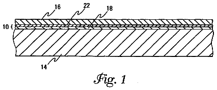
Metal plating using seed film
A seed film and methods incorporating the seed film in semiconductor applications is provided.
US 8,735,186 B2 · Assignee: Semiconductor Energy Laboratory Co., Ltd. · Inventors: Moriwaka; Tomoaki
Sheet 1 of 16 from the published document. All sheets in the USPTO PDF
The energy distribution of the beam spot on the irradiated surface changes due to the change in the oscillation condition of the laser or before and after the maintenance. The present invention provides an optical system for forming a rectangular beam spot on an irradiated surface including a beam homogenizer for homogenizing the energy distribution of the rectangular beam spot on the irradiated surface in a direction of its long or short side. The beam homogenizer includes an optical element having a pair of reflection planes provided oppositely for reflecting the laser beam in the direction where the energy distribution is homogenized and having a curved shape in its entrance surface. The entrance surface of the optical element means a surface of the optical element where the laser beam is incident first.
In recent years, a technique has been extensively researched in which the laser annealing is performed to a non-single crystal semiconductor film (the non-single crystal semiconductor includes an amorphous semiconductor and a semiconductor having crystallinity such as poly-crystal or micro-crystal, which is not single crystal) formed over an insulating substrate such as a glass substrate. It is noted that the laser annealing described herein indicates a technique to recrystallize an amorphous layer or a damaged layer formed in a semiconductor substrate or in the semiconductor film and a technique to crystallise the non-single crystal semiconductor film formed over the substrate. Moreover, a technique applied to planarize or modify a surface of the semiconductor substrate or the semiconductor film is included in the laser annealing. The laser annealing is performed in the crystallization
1 of 16 drawing sheets so far from the published document, cropped to the drawing. Every sheet is in the USPTO PDF.
What the patent claimed, word for word. All of it is now free to use.
The present invention relates to a beam homogenizer to homogenize energy distribution of a beam spot on an irradiated surface in a particular region. Moreover, the present invention also relates to a laser irradiation apparatus using the beam homogenizer. Furthermore, the present invention relates to a method for manufacturing a semiconductor device using the laser irradiation apparatus.
In recent years, a technique has been extensively researched in which the laser annealing is performed to a non-single crystal semiconductor film (the non-single crystal semiconductor includes an amorphous semiconductor and a semiconductor having crystallinity such as poly-crystal or micro-crystal, which is not single crystal) formed over an insulating substrate such as a glass substrate. It is noted that the laser annealing described herein indicates a technique to recrystallize an amorphous layer or a damaged layer formed in a semiconductor substrate or in the semiconductor film and a technique to crystallise the non-single crystal semiconductor film formed over the substrate. Moreover, a technique applied to planarize or modify a surface of the semiconductor substrate or the semiconductor film is included in the laser annealing.
The laser annealing is performed in the crystallization because the glass substrate has a low melting point. The laser can give high energy only to the non-single crystal semiconductor film without changing the temperature of the substrate that much.
It is preferable to perform the laser annealing in such way that a pulsed laser beam having high output such as an excimer laser is shaped into a square spot having a length of several cm on a side or into a rectangular spot having a length of 10 cm or more on a longer side at an irradiated surface through an optical system and that an irradiation position of the beam spot is scanned relative to the irradiated surface because this method can enhance productivity and is superior industrially. Among the rectangular beam spots, a rectangular beam spot having a high aspect ratio is referred to as a linear beam spot in this specification.
In particular, unlike a punctate beam spot requiring to be scanned from front to back and from side to side, the linear beam spot can provide high productivity because the linear beam spot can be irradiated to the large irradiated surface by scanning the linear beam spot only in a direction perpendicular to the long-side direction of the linear beam spot. The laser beam is scanned in the direction perpendicular to the long-side direction of the linear beam spot because it is the most effective way to scan the laser beam. Because of such high productivity, at present, the laser annealing process mainly employs the linear beam spot obtained by shaping the beam spot emitted from a pulsed excimer laser through an appropriate optical system.
FIGS. 12A and 12B show an example of an optical system to transform the sectional shape of the beam spot into linear on the irradiated surface. The optical system shown in FIGS. 12A and 12B is an extremely general optical system. This optical system not only transforms the sectional shape of the beam spot into linear, but also homogenizes the energy distribution of the beam spot on the irradiated surface at the same time. Generally, the optical system for homogenizing the energy distribution of the beam spot is referred to as a beam homogenizer. The optical system shown in FIGS. 12A and 12B is also the beam homogenizer.
When a XeCl excimer laser (having a wavelength 308 nm) is used as a light source, the above optical system is made of quartz. When a laser having a shorter wavelength is used as the light source, the optical system is made of fluorite, MgF.sub.2, or the like.
First, a side view of FIG. 12A is explained. A laser beam emitted from a XeCl excimer laser oscillator 1201 is divided in one direction through cylindrical lens arrays 1202a and 1202b. This direction is herein referred to as a vertical direction. When a mirror is inserted in the optical system, the vertical direction is bent to the direction of the laser beam bent by the mirror. In this structure, the laser beam is divided into four beams. These divided beams are combined into one beam spot once by a cylindrical lens 1204. The beam spots separated again are reflected by a mirror 1206 and then are condensed into one beam spot again on an irradiated surface 1208 by a doublet cylindrical lens 1207. The doublet cylindrical lens is a lens consisting of two cylindrical lenses. This homogenizes the energy distribution of the linear beam spot in the vertical direction and determines the length thereof in the vertical direction.
Next, a top view of FIG. 12B is explained. The laser beam emitted from the laser oscillator 1201 is divided in a direction perpendicular to the vertical direction by a cylindrical lens array 1203. The direction perpendicular to the vertical direction is herein referred to as a horizontal direction. When a mirror is inserted in the optical system, the horizontal direction is bent to the direction of the beam bent by the mirror. In this structure, the laser beam is divided into seven beams. These divided beams are combined into one beam spot by a cylindrical lens 1205 on the irradiated surface 1208. A dotted line shows a correct optical path and correct positions of the lens and the irradiated surface in the case not disposing the mirror 1206. This homogenizes the energy distribution of the linear beam spot in the horizontal direction and determines the length thereof in the horizontal direction.
As described above, the cylindrical lens arrays 1202a, 1202b, and 1203 are the lenses to divide the beam spot of the laser beam. The homogeneity of the energy distribution of the obtained linear beam spot depends on the number of the divided beam spots.
In general, the excimer laser emits a rectangular laser beam having an aspect ratio in the range of approximately 1 to 5. The beam spot of the laser beam has Gaussian distribution where the intensity is higher toward the center. The optical system shown in FIGS. 12A and 12B transforms the beam spot so as to form the beam spot having homogeneous energy distribution and having a size of 320 mm.times.0.4 mm
The linear beam spot shaped by the above structure is irradiated as being overlapped in such a way that the linear beam spot is displaced gradually in the direction of the short side of the linear beam spot. Such an irradiation method makes it possible to perform the laser, annealing to the whole surface of the non-single crystal silicon film to crystallize it or to enhance its crystallinity. In a mass-production factory, at present, the laser annealing is performed to the semiconductor film using the linear beam spot shaped by the optical system as above.
Some beam homogenizers use a reflection mirror. (For example, patent document 1) [Patent Document 1] Japanese Patent Unexamined Publication No. 2001-291681 bulletin
However, a laser irradiation apparatus using the pulsed excimer laser has a problem that, for example, the homogeneity of the energy distribution of the beam spot on the irradiated surface deteriorates because of the fluctuation of a beam axis, which is explained later, or the change in the divergence angle of a laser beam due to the change in the oscillation condition of the excimer laser or due to the cleaning of the window for isolating the gas, which is the laser medium of the excimer laser, from the outside. Therefore, such a laser irradiation apparatus is not yet of high quality for the mass production. The term "beam axis" herein used means a path in which the laser beam travels. The fluctuation or the change of the beam axis means that of the travel direction of the laser beam including the parallel shift of the travel direction of the laser beam.
The present invention is made in view of the above problem, and it is an object of the present invention to provide a beam homogenizer that can suppress as much as possible the change in the energy distribution of the beam spot on the irradiated surface due to the change in the oscillation condition of the excimer laser or due to the maintenance. Moreover, it is an object of the present invention to provide a laser irradiation apparatus and a method for manufacturing a semiconductor device that use the beam homogenizer.
In the present invention, an optical element having a pair of reflection planes provided oppositely and having a curved shape in its entrance surface where the laser beam is incident is used to homogenize the energy distribution of the beam spot on the irradiated surface. As such an optical element, there are a light pipe and an optical waveguide for example. The light pipe is an optical element made of a transparent material having a shape of rectangular solid, circular conic, pyramid, cylinder, or the like, which transmits the light from one end to the other end by the total reflection. The optical waveguide is an optical element that can confine radiation light to a certain region and can transmit the radiation light by guiding the flow of the beam thereof. It is noted that reflection by a mirror may be used to transmit the light. The light pipe belongs to a field of the illumination optics while the optical waveguide belongs to a field of optical communication, which is typified by an optical fiber. Although these two optical elements belong to the different field, it can be said that their optical actions are almost the same.
The present invention discloses a beam homogenizer for shaping a beam spot on an irradiated surface into rectangular. The beam homogenizer includes an optical element for homogenizing energy distribution of the rectangular beam spot in a direction of its long or short side on the irradiated surface, wherein the optical element has a curved shape in the entrance surface where the laser beam is incident and wherein the optical element has a pair of reflection planes provided oppositely. The entrance surface herein means a surface of the optical element where the laser beam is incident first. As the curved shape, a lens is given for example.
In the present invention, the optical element has the curved shape in its entrance surface where the laser beam is incident according to the following reason. When the center axis of the beam axis does not match the center axis of the optical element, the laser beam is incident obliquely into the entrance surface of the optical element. When the laser beam is incident obliquely into the entrance surface of the optical element, the reflection of the laser beam in the optical element is asymmetrical to the center axis of the optical element. Therefore, the energy distribution of the beam spot at the exit surface of the optical element is not sufficiently homogenized. Consequently, the present invention provides the optical element having the curved shape in its entrance surface. With this optical element, the reflection of the laser beam in the optical element can be made symmetrical or near symmetrical to the center axis of the optical element. This can homogenize the energy distribution of the beam spot at the exit of the optical element.
The present invention discloses another beam homogenizer for shaping a beam spot on an irradiated surface into rectangular. This beam homogenizer includes an optical element for homogenizing energy distribution of the rectangular beam spot in a direction of its long or short side on the irradiated surface and includes one or a plurality of cylindrical lenses for projecting a plane having homogeneous energy distribution formed by the optical element to the irradiated surface, wherein the optical element has a curved shape in its entrance surface where the laser beam is incident and wherein the optical element has a pair of reflection planes provided oppositely.
The present invention discloses another beam homogenizer for shaping a beam spot on an irradiated surface into rectangular. This beam homogenizer includes a plurality of optical elements including at least a first optical element for homogenizing energy distribution of the rectangular beam spot in a direction of its long side on the irradiated surface and a second optical element for homogenizing energy distribution of the rectangular beam spot in a direction of its short side on the irradiated surface, wherein each of the first and second optical elements has a curved shape in its entrance surface where the laser beam is incident and wherein the first and second optical elements respectively have a pair of reflection planes provided oppositely.
In the beam homogenizer disclosed in the present invention for shaping a beam spot on an irradiated surface into rectangular, a light pipe or an optical waveguide can be used as the optical element for homogenizing the energy distribution of the rectangular beam spot on the irradiated surface in the direction of its long or short side.
In the beam homogenizer of the present invention for shaping a beam spot on an irradiated surface into rectangular, the curved shape is cylindrical and has curvature in a direction where the optical element acts.
In the present invention, the beam homogenizer shapes a beam spot on the irradiated surface into a rectangular beam spot having an aspect ratio of 10 or more, preferably 100 or more.
The present invention discloses a laser irradiation apparatus for shaping a beam spot on an irradiated surface into rectangular. This laser irradiation apparatus includes a laser oscillator and a beam homogenizer wherein the beam homogenizer includes an optical element for homogenizing energy distribution of the rectangular beam spot in a direction of its long or short side, wherein the optical element has a curved shape in its entrance surface where the laser beam is incident and wherein the optical element has a pair of reflection planes provided oppositely.
The present invention discloses another laser irradiation apparatus for shaping a beam spot on an irradiated surface into rectangular. This laser irradiation apparatus includes a laser oscillator, a beam homogenizer, and one or a plurality of cylindrical lenses for projecting a plane having homogeneous energy distribution formed by the beam homogenizer, wherein the beam homogenizer includes an optical element for homogenizing energy distribution of the rectangular beam spot in a direction of its long or short side, wherein the optical element has a curved shape in its entrance surface where the laser beam is incident, and wherein the optical element has a pair of reflection planes provided oppositely.
The present invention discloses another laser irradiation apparatus for shaping a beam spot on an irradiated surface into rectangular. This laser irradiation apparatus includes a laser oscillator and a beam homogenizer wherein the beam homogenizer includes a plurality of optical elements including at least a first optical element for homogenizing the energy distribution of the rectangular beam spot in a direction of its long side and a second optical element for homogenizing the energy distribution thereof in a direction of its short side, wherein each of the first and the second optical elements has a curved shape in its entrance surface where the laser beam is incident, and wherein the first and second optical elements respectively have a pair of reflection planes provided oppositely.
In the laser irradiation apparatus disclosed in the present invention, a light pipe or an optical waveguide can be used as the optical element for homogenizing the energy distribution of the rectangular beam spot on the irradiated surface in the direction of its long or short side.
In the above laser irradiation apparatus of the present invention, the curved shape is cylindrical shape and has the curvature in a direction where the optical element acts.
The laser irradiation apparatus of the present invention shapes a beam spot on the irradiated surface into a rectangular beam spot having an aspect ratio of 10 or more, preferably 100 or more.
The laser irradiation apparatus of the present invention has a scanning stage for moving an irradiated object having an irradiated surface relative to a beam spot and has an automatic transferring apparatus for transferring the irradiated object having the irradiated surface to the scanning stage.
In the laser irradiation apparatus of the present invention, the laser oscillator is one selected from the group consisting of an excimer laser, a YAG laser, a glass laser, a YVO.sub.4 laser, a YLF laser, an Ar laser, and a GdVO.sub.4 laser.
The present invention discloses a method for manufacturing a semiconductor device including the steps of forming a non-single crystal semiconductor film over a substrate and performing laser annealing in such a way that a laser beam which is emitted from a laser oscillator and which is shaped into a rectangular beam spot on the non-single crystal semiconductor film through an optical system including an optical element for homogenizing energy distribution of the rectangular beam spot is irradiated to the non-single crystal semiconductor while moving a position of the beam spot, wherein the optical element acts on a direction of a long or short side of the rectangular beam spot, wherein the optical element has a curved shape in its entrance surface where the laser beam is incident, and wherein the optical element has a pair of reflection planes provide oppositely.
The present invention discloses another method for manufacturing a semiconductor device comprising the steps of forming a non-single crystal semiconductor film over a substrate and performing laser annealing in such a way that a laser beam which is emitted from a laser oscillator and which is shaped into a rectangular beam spot on the non-single crystal semiconductor film through an optical system including an optical element for homogenizing energy distribution of a rectangular beam spot and one or a plurality of cylindrical lenses for projecting a plane having the homogeneous energy distribution formed by the optical element to the non-single crystal semiconductor film is irradiated to the non-single crystal semiconductor film while moving a position of the beam spot wherein optical element acts on a direction of a long or short side of the rectangular beam spot, wherein the optical element has a curved shape in its entrance surface where the laser beam is incident, and wherein the optical element has a pair of reflection planes provided oppositely.
The present invention discloses another method for manufacturing a semiconductor device including the steps of forming a non-single crystal semiconductor film over a substrate and performing laser annealing in such a way that a laser beam which is emitted from a laser oscillator and which is shaped into a rectangular beam spot on the non-single crystal semiconductor film through an optical system including a plurality of optical elements is irradiated to the non-single crystal semiconductor film while moving a position of the beam spot wherein the plurality of optical elements includes at least a first optical element acting on a direction of its long side of the rectangular beam spot and a second optical element acting on a direction of its short side of the rectangular beam spot, wherein each of the first and second optical elements has a curved shape in its entrance surface where the laser beam is incident, and wherein the first and second optical elements respectively have a pair of reflection planes provided oppositely.
In the method for manufacturing a semiconductor device of the present invention, a light pipe or an optical waveguide can be used instead of an optical element to homogenize the energy distribution of the rectangular beam spot on the irradiated surface in a direction of its short side in the optical system for forming a rectangular beam spot.
In the method for manufacturing a semiconductor device of the present invention, the curved shape is cylindrical and has the curvature in a direction where the optical element acts.
In the method for manufacturing a semiconductor device of the present invention, the rectangular beam spot formed on the irradiated surface has an aspect ratio of 10 or more, preferably 100 or more.
In the method for manufacturing a semiconductor device of the present invention, the laser oscillator is one selected from the group consisting of an excimer laser, a YAG laser, a glass laser, a YVO.sub.4 laser, a YLF laser, an Ar laser, and a GdVO.sub.4 laser.
Advantageous Effect of the Invention
When the beam homogenizer including the optical element that homogenizes the energy distribution of the laser beam and that has a curved shape in its entrance surface where the laser beam is incident for forming a rectangular beam spot disclosed in the present invention is used, it is possible to form a rectangular beam spot having homogeneous energy distribution on the irradiated surface. Moreover, since the position and the energy distribution of the beam spot formed on the irradiated surface are not easily affected by the oscillation condition of the laser oscillator, it is possible to keep the shape of the beam spot stably.
When the rectangular beam spot emitted from the laser irradiation apparatus using the beam homogenizer of the present invention is scanned on a semiconductor film in a direction of its short side, it is possible to suppress the inhomogeneous crystallinity due to the inhomogeneous energy distribution of the beam spot and to improve the homogeneity of the crystallinity in the surface of the substrate. Moreover, according to the present invention, the laser irradiation apparatus can obtain the high stability. Furthermore, since it is possible to do the maintenance more easily, the running cost can be reduced. With the present invention applied to the mass production line of the poly-silicon TFT, a TFT having high operating characteristic uniformly can be manufactured efficiently. Moreover, when the poly-silicon TFT manufactured by the present invention is applied to a liquid crystal display device and a light-emitting device using a light-emitting element typified by an EL element, it is possible to manufacture a display device having almost no display unevenness.
In the accompanying drawings:
FIG. 1 is a drawing for explaining the beam homogenizer of the present invention;
FIG. 2 is a drawing for explaining the conventional beam homogenizer;
FIGS. 3A and 3B are drawings for showing an example of the laser irradiation apparatus including the beam homogenizer disclosed in the present invention;
FIGS. 4A and 4B are drawings for showing an example of the laser irradiation, apparatus including the beam homogenizer disclosed in the present invention;
FIGS. 5A to 5C are drawings for showing the energy distribution of the beam spot;
FIGS. 6A and 6B are drawings for showing an example of the laser irradiation apparatus including the beam homogenizer disclosed in the present invention;
FIGS. 7A and 7B are drawings for showing an example of the laser irradiation apparatus including the beam homogenizer disclosed in the present invention;
FIGS. 8A and 8B are drawings for showing an example of the laser irradiation apparatus including the beam homogenizer disclosed in the present invention;
FIG. 9 is a drawing for showing the energy distribution of the beam spot;
FIGS. 10A and 10B are drawings for showing an example of the laser irradiation apparatus including the beam homogenizer disclosed in the present invention;
FIGS. 11A and 11B are drawings for explaining the homogenization of the energy distribution by the optical waveguide;
FIGS. 12A and 12B are drawings for explaining the related art;
FIGS. 13A and 13B are drawings for showing the energy distribution of the beam spot;
FIGS. 14A and 14B are drawings for showing the energy distribution of the beam spot;
FIGS. 15A and 15B are drawings for showing the energy distribution of the beam spot;
FIG. 16 is a drawing for explaining the incidence angle of the laser beam; and
FIGS. 17A and 17B are drawings for showing an example of the laser irradiation apparatus including the beam homogenizer disclosed in the present invention.
Hereinafter, an embodiment mode and embodiments of the present invention are explained based on drawings. However, since the present invention can be embodied in many different modes, it is easily understood by those skilled in the art that the modes and the details of the present invention can be changed and modified in various ways unless such changes and modifications depart from the scope and the content of the present invention hereinafter defined. Thus, the present invention is not limited to the description of the embodiment mode and the embodiments. It is noted that the same reference numeral is used to indicate the same thing throughout the drawings of the present invention.
First, the method to homogenize the energy distribution of the beam spot by the optical element having a pair of reflection planes provided oppositely for reflecting the laser beam in the direction where the energy distribution of the beam spot is homogenized is explained with reference to FIGS. 11A and 11B. A top view of FIG. 11A is explained first. There are an optical element 1102 having a pair of reflection planes 1102a and 1102b provided oppositely and an irradiated surface 1103 in FIG. 11A. The ray is made incident from the left side on the paper. The ray is drawn with a continuous line 1101a when there is the optical element 1102 and is drawn with a dotted line 1101b when there is not the optical element 1102. When there is not the optical element 1102, the ray incident from the left side on the paper reaches regions 1103a, 1103b, and 1103c in the irradiated surface 1103 as shown with the dotted line 1101b.
On the other hand, when there is the optical element 1102, the ray is reflected by the reflection planes of the optical element 1102 as shown with the ray 1101a, and then all the rays reach a region 1103b in the irradiated surface 1103. That is to say, when there is the optical element 1102, all the rays that reach the regions 1103a and 1103c when there is not the optical element 1102 reach the region 1103b in the irradiated surface 1103. Therefore, when the rays are made incident into the optical element 1102, the rays are reflected repeatedly and are led to the exit. That is to say, the rays are superposed in the same position as if the incident rays are folded on the region 1103b in the irradiated surface 1103. In this example, the total divergence of the rays 1103a, 1103b, and 1103c on the irradiated surface 1103 when there is not the optical element is defined as A, and the divergence of the ray 1103b on the irradiated surface 1103 when there is the optical element is defined as B. Then, A/B corresponds to the number of rays divided by the homogenizer. Thus, when the incident ray is divided and all the divided rays are superposed on the same position, the energy distribution of the ray is homogenized on the superposed position.
In general, the more the homogenizer divides the ray, the more homogeneous the energy distribution becomes on the position where the divided rays are superposed. The number of divisions by the optical element 1102 can be increased when the ray is reflected more times in the optical element 1102. In other words, the length of the pair of reflection planes in the direction where the rays are incident may be made longer. Moreover, the number of divisions can be increased by narrowing the space between the reflection planes provided oppositely or by increasing NA (numerical aperture) of the ray incident into the optical element.
The light pipe or the optical waveguide, having a pair of reflection planes provided oppositely for reflecting the laser beam in the direction where the energy distribution of the beam spot is homogenized, can be used as the optical element to homogenize the energy distribution of the ray.
The optical system for forming a rectangular beam spot disclosed in the present invention is explained with reference to FIGS. 3A and 3B. First, a side view of FIG. 3B is explained. A laser beam emitted from a laser oscillator 301 propagates in a direction indicated by an arrow in FIGS. 3A and 3B. The laser beam is expanded by spherical lenses 302a and 302b. The spherical lenses 302a and 302b are not required in the case where the beam spot emitted from the laser oscillator 301 is sufficiently large.
The direction of the long side hereinafter means the direction of the long side of the rectangular beam spot formed on the irradiated surface 307. The direction of the short side hereinafter means the direction of the short side of the rectangular beam spot formed on the irradiated surface 307. The laser beam is focused by a cylindrical lens 304 in a direction of the short side and is incident into an optical element 305 positioned behind the cylindrical lens 304, having a pair of reflection planes provided oppositely for reflecting the laser beam in the direction where the energy distribution of the beam spot is homogenized. The entrance surface of the optical element 305 has cylindrical curvature in a direction of the short side, which means the direction where the energy distribution is homogenized. The laser beam is totally reflected in the light pipe repeatedly and is led to the exit. Then, a plane having homogeneous energy distribution in a direction of the short side of the rectangular beam spot is formed at an exit surface of the optical element 305. Here, the exit surface means a surface of the optical element from which the laser beam is emitted. It is necessary to determine the curvature of the cylindrical lens 304 so that the laser beam is totally reflected at the interface between the optical element 305 and the air.
The reason why the optical element 305 has the curvature in the entrance surface thereof is explained with reference to FIGS. 1 and 2. FIGS. 1 and 2 are the drawings observed from a direction perpendicular to the direction where the energy distribution is homogenized. In FIGS. 1 and 2, a laser beam emitted from a laser oscillator (not shown diagrammatically) is focused by cylindrical lenses 101 and 201 so that the laser beam is incident into optical elements 102 and 202. The incidence position of the laser beam is not the center of the cylindrical lenses 101 and 201 in both FIGS. 1 and 2, and the focal points are not on the center axis of the optical elements 102 and 202, having a pair of reflection planes provided oppositely for reflecting the laser beam in the direction where the energy distribution of the beam spot is homogenized. The laser beams are incident obliquely at a certain angle into the optical elements 102 and 202.
In FIG. 2, the laser beam is focused by the cylindrical lens 201 and is incident into the optical element 202 obliquely. After that, the laser beam is reflected repeatedly in the optical element asymmetrically to the center axis of the light pipe and is led to the exit. Thus, a beam spot having inhomogeneous energy distribution is formed at the exit surface of the optical element. On the other band, in FIG. 1, after the laser beam is focused by the cylindrical lens 101, the laser beam is incident into the optical element 102 having the curved shape in the entrance surface thereof. When the optical element has the curved shape in the entrance surface, the laser beam incident obliquely into the optical element expanded to correct the reflection of the laser beam incident into the optical element so that the reflection becomes symmetrical or near symmetrical to the center axis of the optical element. This can form the beam spot having homogeneous energy distribution at the exit surface of the optical element.
The curvature of the curved shape is determined based on the specification of the optical system in the previous paragraph such as the incidence angle and the length and the width of the optical element.
As described above, when the optical element having the curved shape in its entrance surface is used, the energy distribution of the beam spot formed by the optical element can be kept homogeneous even though the beam axis changes for every pulse oscillation or even though the beam axis changes due to the maintenance or due to the effect of the pointing stability of the laser beam emitted from the laser oscillator. Moreover, with the optical element, the position of the plane having homogeneous energy distribution can be fixed completely by the optical system. This makes it possible to obtain the laser beam having homogeneous energy distribution that is not affected by the condition of the laser oscillator on the irradiated surface.
The longer the optical element 305 is in the direction where the laser beam is incident or the shorter the focal length of the cylindrical lens 304 is, the more homogeneous the energy distribution becomes. However, since the actual system must be manufactured in consideration of the size of the optical system, it is necessary that the length of the light pipe and the focal length are practical in accordance with the size of the system.
In FIGS. 3A and 3B, a doublet cylindrical lens 306 positioned behind the optical element 305 projects the plane having homogeneous energy distribution formed at the exit surface of the optical element 305 to an irradiated surface 307 positioned behind the doublet cylindrical lens. The doublet cylindrical lens 306 is a lens consisting of two cylindrical lenses 306a and 306b. This projects the plane having homogeneous energy distribution formed at the exit surface of the optical element 305 to another surface (irradiated surface). In other words, the plane having homogeneous energy distribution and the irradiated surface 307 are in the conjugated position with respect to the doublet cylindrical lens 306. The optical element 305 and the doublet cylindrical lens 306 homogenize the energy distribution of the rectangular beam spot in the direction of its short side and determine the length thereof in the direction of its short side. In addition, when the homogeneity of the energy distribution of the beam spot at the irradiated surface is not required that much or when the F-number (F=focal length of the lens/diameter of the entrance pupil) of the doublet cylindrical lens is extremely large, a singlet cylindrical lens may be used.
Next, a top view of FIG. 3A is explained. A beam spot of a laser beam emitted from a laser oscillator 301 is divided by a cylindrical lens array 303 in a direction of a long side. The cylindrical lens array 303 has a plurality of cylindrical lenses arranged in a direction of its curvature. In the present embodiment mode, five cylindrical lenses are arranged in the cylindrical lens array. This homogenizes the energy distribution of the rectangular beam spot in a direction of its long side and determines the length thereof in the direction of its long side. It is noted that a cylindrical lens for combining the laser beams divided by the cylindrical lens array may be provided behind the cylindrical lens array.
The laser oscillator used in combination with the beam homogenizer of the present invention preferably has high output power and has a wavelength region that is sufficiently absorbed in the semiconductor film. In the case of using a silicon film as the semiconductor film, the laser beam emitted from the laser oscillator preferably has a wavelength of 600 nm or shorter in consideration of the absorption coefficient. As the laser oscillator emitting such a wavelength, there are an excimer laser, a YAG laser (harmonic), and a glass laser (harmonic), for example.
In addition, although high output power is not yet obtained by the current technology, a YVO.sub.4 laser (harmonic), a YLF laser (harmonic), an Ar laser, and an GdVO.sub.4 are given for example as the laser oscillator emitting the laser beam having a wavelength appropriate for crystallizing the silicon film.
The optical system disclosed in the present invention may be used under the atmosphere or may be used under a nitrogen or Ar atmosphere in order to minimize the damage of the light pipe and the surface of the lens due to the laser beam having high energy.
Although this embodiment mode explains the optical element having a pair of reflection planes provided oppositely to homogenize the energy distribution of the beam spot, the light pipe or the optical waveguide may be also used because they have the similar optical advantageous effect.
Hereinafter a method for manufacturing a semiconductor device using the beam homogenizer and the laser irradiation apparatus of the present invention is explained. A glass substrate having enough resistance against the heat up to 600.degree. C. is used as the substrate. A silicon oxide film is formed on the glass substrate as a base film, and a non-single crystal silicon film is formed thereon. These films are formed by a sputtering method or a plasma CVD method.
The substrate with the films formed thereon is heated under the nitrogen atmosphere to decrease the concentration of hydrogen in the non-single crystal silicon film. This process is performed because the film cannot resist the laser power when the film contains too much hydrogen. The concentration of hydrogen in the film is appropriate on the order of 10.sup.20 atoms/cm.sup.3. Here, 10.sup.20 atoms/cm.sup.3 means that 10.sup.20 hydrogen atoms exist in 1 cm.sup.3. The processing time and the temperature of the substrate in this heating process may be determined by a practitioner appropriately. However, the heating temperature must be determined in consideration of the resistivity of the glass substrate.
This embodiment mode employs a XeCl excimer laser as the laser oscillator. The excimer laser is a pulsed laser oscillator. When the power of the pulsed laser beam fluctuates within .+-.5%, preferably within .+-.2%, in each pulse during the laser processing performed to one substrate, it is possible to perform homogeneous crystallization. It is noted that the lenses and the optical element that has a curved shape in its entrance surface for homogenizing the energy distribution of the laser beam shown in the present embodiment mode are made of the synthetic quartz having high transmittance and resistance to the XeCl excimer laser.
The fluctuation of the laser power described above is defined as follows. The average value of the laser power in the period of the irradiation to one substrate is assumed to be standard. Then, the fluctuation of the laser power is defined as the value expressing the difference between the average value and the maximum or minimum value in the period of the irradiation in percentage terms.
The laser beam is irradiated in such a way that a stage with the irradiated surface 307 shown in FIGS. 3A and 3B mounted thereon is scanned in the direction of the short side of the rectangular beam spot. On this occasion, a practitioner may determine the energy density and the scanning speed of the beam spot on the irradiated surface appropriately. The energy density is appropriate in the range of 200 to 1000 mJ/cm.sup.2. It is feasible to perform laser annealing homogeneously when the scanning speed is selected in the range where the width of the rectangular beam spot in its short side is overlapped one another by 80% or more, preferably by approximately 90%. The optimum scanning speed depends on the pulse repetition rate of the laser oscillator and it may be regarded to be proportional to the pulse repetition rate thereof.
The description continues in the full USPTO document.
About 6,600 words. The USPTO PDF has it with every drawing.
Fees are due 3.5, 7.5 and 11.5 years after grant. This patent expired on May 27, 2026, so the fee marked "not paid" was the one that went unpaid.
Beam homogenizer, laser irradiation apparatus, and method for manufacturing semiconductor device
Filed Sep 2004 · published Apr 2005Beam homogenizer, laser irradiation apparatus, and method for manufacturing semiconductor device
Filed Sep 2004 · granted Jan 2007Beam homogenizer, laser irradiation apparatus, and method for manufacturing semiconductor device
Filed Jan 2007 · published May 2007Beam homogenizer, laser irradiation apparatus, and method for manufacturing semiconductor device
Filed Jan 2007 · granted Jul 2011BEAM HOMOGENIZER, LASER IRRADIATION APPARATUS, AND METHOD FOR MANUFACTURING SEMICONDUCTOR DEVICE
Filed Jun 2011 · published Oct 2011Beam homogenizer, laser irradiation apparatus, and method for manufacturing semiconductor device
Filed Jun 2011 · granted Jan 2014BEAM HOMOGENIZER, LASER IRRADIATION APPARATUS, AND METHOD FOR MANUFACTURING SEMICONDUCTOR DEVICE
Filed Dec 2013 · published Apr 2014Beam homogenizer, laser irradiation apparatus, and method for manufacturing semiconductor device
Filed Dec 2013 · granted May 2014Earlier publications, parents and continuations. None of them can still be enforced, or this patent would not be listed.
Prior art cited by the examiner or applicant. Useful when you check your own idea for novelty.
Everything on this page comes from the documents linked above.


