 Lapsed, fee not paid5 drawings
Hardware & Electronics · US 8,730,679 B2
Electrically connecting module
An electrically connecting module suitable for an electronic device is provided.
US 8,730,722 B2 · Assignee: SanDisk Technologies Inc. · Inventors: Koh; Pao-Ling et al.
Sheet 1 of 27 from the published document. All sheets in the USPTO PDF
Technique of operating a non-volatile memory are presented so that in case data that would otherwise be lost in the case of a word line to word line short is preserved. Before writing a word line, the data from a previously written adjacent is word line is read back and stored in data latches associated with the corresponding bit lines, but that are not being used for the data to be written. If a short occurs, as the data for both word lines is still in the latches, it can be written to a new location. This technique can also be incorporated into cache write operations and for a binary write operation inserted into a pause of a multi-state write.
Solid-state memory capable of nonvolatile storage of charge, particularly in the form of EEPROM and flash EEPROM packaged as a small form factor card, has recently become the storage of choice in a variety of mobile and handheld devices, notably information appliances and consumer electronics products. Unlike RAM (random access memory) that is also solid-state memory, flash memory is non-volatile and retains its stored data even after power is turned off. In spite of the higher cost, flash memory is increasingly being used in mass storage applications. Conventional mass storage, based on rotating magnetic medium such as hard drives and floppy disks, is unsuitable for the mobile and handheld environment. This is because disk drives tend to be bulky, are prone to mechanical failure and have high latency and high power requirements. These undesirable attributes make disk-based storage impra
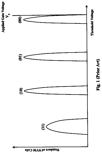
1 of 27 drawing sheets so far from the published document, cropped to the drawing. Every sheet is in the USPTO PDF.
What the patent claimed, word for word. All of it is now free to use.
This invention relates generally to semiconductor memory circuits such as electrically erasable programmable read-only memory (EEPROM) and flash EEPROM, and specifically to the detection of, and recovery of data from, defective word-lines in such memory circuits.
Solid-state memory capable of nonvolatile storage of charge, particularly in the form of EEPROM and flash EEPROM packaged as a small form factor card, has recently become the storage of choice in a variety of mobile and handheld devices, notably information appliances and consumer electronics products. Unlike RAM (random access memory) that is also solid-state memory, flash memory is non-volatile and retains its stored data even after power is turned off. In spite of the higher cost, flash memory is increasingly being used in mass storage applications. Conventional mass storage, based on rotating magnetic medium such as hard drives and floppy disks, is unsuitable for the mobile and handheld environment. This is because disk drives tend to be bulky, are prone to mechanical failure and have high latency and high power requirements. These undesirable attributes make disk-based storage impractical in most mobile and portable applications. On the other hand, flash memory, both embedded and in the form of a removable card, are ideally suited in the mobile and handheld environment because of its small size, low power consumption, high speed and high reliability features.
EEPROM and electrically programmable read-only memory (EPROM) are non-volatile memory that can be erased and have new data written or "programmed" into their memory cells. Both utilize a floating (unconnected) conductive gate, in a field effect transistor structure, positioned over a channel region in a semiconductor substrate, between source and drain regions. A control gate is then provided over the floating gate. The threshold voltage characteristic of the transistor is controlled by the amount of charge that is retained on the floating gate. That is, for a given level of charge on the floating gate, there is a corresponding voltage (threshold) that must be applied to the control gate before the transistor is turned "on" to permit conduction between its source and drain regions.
The floating gate can hold a range of charges and therefore can be programmed to any threshold voltage level within a threshold voltage window. The size of the threshold voltage window is delimited by the minimum and maximum threshold levels of the device, which in turn correspond to the range of the charges that can be programmed onto the floating gate. The threshold window generally depends on the memory device's characteristics, operating conditions and history. Each distinct, resolvable threshold voltage level range within the window may, in principle, be used to designate a definite memory state of the cell. When the threshold voltage is partitioned into two distinct regions, each memory cell will be able to store one bit of data. Similarly, when the threshold voltage window is partitioned into more than two distinct regions, each memory cell will be able to store more than one bit of data.
In the usual two-state EEPROM cell, at least one current breakpoint level is established so as to partition the conduction window into two regions. When a cell is read by applying predetermined, fixed voltages, its source/drain current is resolved into a memory state by comparing with the breakpoint level (or reference current IREF). If the current read is higher than that of the breakpoint level, the cell is determined to be in one logical state (e.g., a "zero" state). On the other hand, if the current is less than that of the breakpoint level, the cell is determined to be in the other logical state (e.g., a "one" state). Thus, such a two-state cell stores one bit of digital information. A reference current source, which may be externally programmable, is often provided as part of a memory system to generate the breakpoint level current.
In order to increase memory capacity, flash EEPROM devices are being fabricated with higher and higher density as the state of the semiconductor technology advances. Another method for increasing storage capacity is to have each memory cell store more than two states.
For a multi-state or multi-level EEPROM memory cell, the conduction window is partitioned into more than two regions by more than one breakpoint such that each cell is capable of storing more than one bit of data. The information that a given EEPROM array can store is thus increased with the number of states that each cell can store. EEPROM or flash EEPROM with multi-state or multi-level memory cells have been described in U.S. Pat. No. 5,172,338.
The transistor serving as a memory cell is typically programmed to a "programmed" state by one of two mechanisms. In "hot electron injection," a high voltage applied to the drain accelerates electrons across the substrate channel region. At the same time a high voltage applied to the control gate pulls the hot electrons through a thin gate dielectric onto the floating gate. In "tunneling injection," a high voltage is applied to the control gate relative to the substrate. In this way, electrons are pulled from the substrate to the intervening floating gate.
The memory device may be erased by a number of mechanisms. For EPROM, the memory is bulk erasable by removing the charge from the floating gate by ultraviolet radiation. For EEPROM, a memory cell is electrically erasable, by applying a high voltage to the substrate relative to the control gate so as to induce electrons in the floating gate to tunnel through a thin oxide to the substrate channel region (i.e., Fowler-Nordheim tunneling.) Typically, the EEPROM is erasable byte by byte. For flash EEPROM, the memory is electrically erasable either all at once or one or more blocks at a time, where a block may consist of 512 bytes or more of memory.
The memory devices typically comprise one or more memory chips that may be mounted on a card. Each memory chip comprises an array of memory cells supported by peripheral circuits such as decoders and erase, write and read circuits. The more sophisticated memory devices operate with an external memory controller that performs intelligent and higher level memory operations and interfacing.
There are many commercially successful non-volatile solid-state memory devices being used today. These memory devices may be flash EEPROM or may employ other types of nonvolatile memory cells. Examples of flash memory and systems and methods of manufacturing them are given in U.S. Pat. Nos. 5,070,032, 5,095,344, 5,315,541, 5,343,063, and 5,661,053, 5,313,421 and 6,222,762. In particular, flash memory devices with NAND string structures are described in U.S. Pat. Nos. 5,570,315, 5,903,495, 6,046,935. Also nonvolatile memory devices are also manufactured from memory cells with a dielectric layer for storing charge. Instead of the conductive floating gate elements described earlier, a dielectric layer is used. Such memory devices utilizing dielectric storage element have been described by Eitan et al., "NROM: A Novel Localized Trapping, 2-Bit Nonvolatile Memory Cell," IEEE Electron Device Letters, vol. 21, no. 11, November 2000, pp. 543-545. An ONO dielectric layer extends across the channel between source and drain diffusions. The charge for one data bit is localized in the dielectric layer adjacent to the drain, and the charge for the other data bit is localized in the dielectric layer adjacent to the source. For example, U.S. Pat. Nos. 5,768,192 and 6,011,725 disclose a nonvolatile memory cell having a trapping dielectric sandwiched between two silicon dioxide layers. Multi-state data storage is implemented by separately reading the binary states of the spatially separated charge storage regions within the dielectric.
Defects often occur in such memory systems, both as part of the manufacturing process as well over the operating life of the device. One of the sources of such defects are the word-lines of such memory arrays, due both to word-line leakage (to another word-line or to the substrate) and to broken word-lines. These word-line related problems typically become more and more acute as device sizes scale down. Some word-line to word-line leakage does not manifest itself when the device is fresh, but only results in a failure after the stress of a number of program-erase cycles. This leakage will cause the faulty word-line to fail to program and corresponding data will be corrupted. A broken word-line will have a high resistive connection, as a result of which the cells on far end of the break will see a voltage drop during program and verify operations. As a result, the threshold voltage distribution for the broken word-line will show un-distinguishable states. Consequently, both of these sorts of defects can be detrimental to memory operation if not detected. In the case of a word line to word line short, although such a defect may be detected by the program status, even if detected the data for both the data begin written and the previously programmed word line data can be lost.
According to a first set of aspects, a method of operating a non-volatile memory device is presented. The memory device includes an array of non-volatile memory cells formed along a plurality of bit lines and a plurality of word lines and, for each of the bit lines, a corresponding plurality of data latches connected to them whereby multi-state can be programmed into a selected word line according to data held in the corresponding data latches. The method includes receiving a first page of data and storing the received first page of data in a first of the data latches for each of the corresponding bit lines. The first page of data is written from the first of the data latches into a first word line in a binary format. After storing the received first page of data in the first of the data latches for each of the corresponding bit lines, a second page of data is received. After writing the first page of data into the first word line and receiving the second page of data, the first page of data is read from the first word line into a second of the data latches for each of the corresponding bit lines. Subsequent to writing the first page of data into the first word line, the received second page of data is stored in a third of the data latches for each of the corresponding bit lines, where the third of the data latches is different from the second of the data latches for each of the corresponding bit lines. The second page of data is written from the third of the data latches into a second word line in a binary format, where the second word line is adjacent to the first word line. After writing the second page of data into the second word line, the first page of data is held in the second of the data latches for each of the corresponding bit lines and the second page of data is held in the third of the data latches for each of the corresponding bit lines.
In other aspects, a method of operating a non-volatile memory device is presented. The memory device includes an array of non-volatile memory cells formed along a plurality of bit lines and a plurality of word lines and, for each of the bit lines, has a corresponding plurality of data latches connected to the bit lines whereby multi-state can be programmed into a selected word line according to data held in the corresponding data latches. The method includes: receiving and storing a first page of data in a first of the data latches for each of the corresponding bit lines; transferring the first page of data from the first of the data latches into a second of the data latches for each of the corresponding bit lines; and writing the first page of data from the second of the data latches into a first word line in a binary format. The method further includes receiving and storing a second page of data in the first of the data latches for each of the corresponding bit lines and, subsequent to writing the first page of data into the first word line, transferring the first page of data from the second of the data latches into a third of the data latches for each of the corresponding bit lines. Subsequent to transferring the first page of data into the third of the data latches for each of the corresponding bit lines, the second page of data is transferred from the first of the data latches into the second of the data latches for each of the corresponding bit lines. A third page of data is subsequently received and stored in the first of the data latches for each of the corresponding bit lines. The second page of data is written from the second of the data latches into a second word line in a binary format, where the second word line is adjacent to the first word line. Subsequent to writing the second page of data into the second word line, the first page of data is held in the third of the data latches for each of the corresponding bit lines, the second page of data is held in the second of the data latches for each of the corresponding bit lines, and the third page age of data is held in the first of the data latches for each of the corresponding bit lines.
In further aspects, a method of operating a non-volatile memory device. The memory device includes an array of non-volatile memory cells formed along a plurality of bit lines and a plurality of word lines and, for each of the bit lines, has a corresponding plurality of (N+2) data latches connected thereto whereby multi-state can be programmed into a selected word line according to data held in the corresponding data latches. N is an integer 2 or greater. The method includes initiating a N-state write operation into a first word line for N pages of data from N of the data latches for each of the corresponding bit lines using an (N+1)st of the data latches of the corresponding bit lines to partially inhibit programming in response to verifying at a low verify level and subsequently suspending the N-state write operation while maintaining the N pages of data in the N of the data latches for each of the corresponding bit lines. While the N-state write operation is suspended and while maintaining the N pages of data in the N of the data latches for each of the corresponding bit line, the method also includes: reading a first page of binary data written in binary format from a second word line into the (N+1)st of the data latches of the corresponding bit lines overwriting the content thereof, wherein the first and second word lines are different; receiving in the (N+2)nd of the data latches of the corresponding bit lines a second page of binary data; and subsequently writing in a binary format the second page of binary data from the (N+2)nd of the data latches of the corresponding bit lines into a third word line adjacent to the second word line while maintaining the first page of binary in the (N+1)st of the data latches of the corresponding bit lines, where the third word line is different than the first word line. The N-state write operation is subsequently resumed and includes reestablishing the content of the (N+1)st of the data latches of the corresponding bit lines.
Various aspects, advantages, features and embodiments of the present invention are included in the following description of exemplary examples thereof, whose description should be taken in conjunction with the accompanying drawings. All patents, patent applications, articles, other publications, documents and things referenced herein are hereby incorporated herein by this reference in their entirety for all purposes. To the extent of any inconsistency or conflict in the definition or use of terms between any of the incorporated publications, documents or things and the present application, those of the present application shall prevail.
FIG. 1 illustrates schematically the functional blocks of a non-volatile memory chip in which the present invention may be implemented.
FIG. 2 illustrates schematically a non-volatile memory cell.
FIG. 3 illustrates the relation between the source-drain current I.sub.D and the control gate voltage V.sub.CG for four different charges Q1-Q4 that the floating gate may be selectively storing at any one time.
FIG. 4 illustrates an example of an NOR array of memory cells.
FIG. 5A illustrates schematically a string of memory cells organized into an NAND string.
FIG. 5B illustrates an example of an NAND array 200 of memory cells, constituted from NAND strings 50 such as that shown in FIG. 5A.
FIG. 6 illustrates the Read/Write Circuits 270A and 270B, shown in FIG. 1, containing a bank of p sense modules across an array of memory cells.
FIG. 7 illustrates schematically a preferred organization of the sense modules shown in FIG. 6.
FIG. 8 illustrates in more detail the read/write stacks shown in FIG. 7.
illustrate an example of programming a population of 4-state memory cells.
illustrate an example of programming a population of 8-state memory cells.
FIG. 11 illustrates a conventional technique for programming a 4-state memory cell to a target memory state.
FIG. 12 shows a circuitry detail on how voltages are supplied to word-lines.
FIG. 13 is a block diagram of an exemplary charge pump circuit.
FIG. 14 adds leakage detection circuitry to FIG. 13.
FIG. 15 illustrates the phases of the exemplary leakage detection operation.
FIG. 16 shows the current path in a calibration process for the word-line leakage process.
FIG. 17 illustrates the phases of the calibration operation.
FIG. 18 shows the distribution of memory cell threshold voltage values to illustrate symptoms of a broken word-line.
FIG. 19 illustrates the variation in the number of programming pulse-verify iterations over different word-lines.
FIG. 20 is a timing diagram for a broken word-line detection routine.
FIGS. 21A and 21B illustrate differing placements of word-line drivers.
FIGS. 22 and 23A are flows for a scan of failed bits in a program operation.
FIG. 23B is a flow for a scan of failed bits in a program operation that also includes broken word-line detection.
FIG. 24 illustrates a current based comparison for leakage determination where two different arrays are used, one unselected and for reference use and one with an erase block selected for testing.
FIG. 25 illustrates the basic operation of exemplary circuitry for determining a leakage current level.
FIG. 26 shows the elements from FIG. 25 along with some to the other elements used in the exemplary embodiment for the leakage determination circuitry.
FIG. 27 is a block diagram to schematically illustrate the relationship of the elements of FIG. 26 to two planes.
FIG. 28 is a timing diagram for one particular implementation of the leakage determination operation.
FIG. 29 adds leakage current determination elements to the part of the waveform of FIG. 28.
FIGS. 30A and 30B respectively illustrate a flow for a binary programming operation that saves a copy of the previously written page of data in the data latches and content of the latches during the operation.
FIGS. 31A and 31B respectively illustrate a flow for a binary cache programming operation that saves a copy of the previously written page of data in the data latches and content of the latches during the operation.
FIGS. 32A and 32B respectively illustrate a flow for a binary programming operation performed during a suspended multi-state write that saves a copy of the previously written page of data in the data latches and content of the latches during the operation.
Memory System
FIG. 1 to FIG. 11 illustrate example memory systems in which the various aspects of the present invention may be implemented.
FIG. 1 illustrates schematically the functional blocks of a non-volatile memory chip in which the present invention may be implemented. The memory chip 100 includes a two-dimensional array of memory cells 200, control circuitry 210, and peripheral circuits such as decoders, read/write circuits and multiplexers.
The memory array 200 is addressable by word lines via row decoders 230 (split into 230A, 230B) and by bit lines via column decoders 260 (split into 260A, 260B) (see also FIGS. 4 and 5.) The read/write circuits 270 (split into 270A, 270B) allow a page of memory cells to be read or programmed in parallel. A data I/O bus 231 is coupled to the read/write circuits 270.
In a preferred embodiment, a page is constituted from a contiguous row of memory cells sharing the same word line. In another embodiment, where a row of memory cells are partitioned into multiple pages, block multiplexers 250 (split into 250A and 250B) are provided to multiplex the read/write circuits 270 to the individual pages. For example, two pages, respectively formed by odd and even columns of memory cells are multiplexed to the read/write circuits.
FIG. 1 illustrates a preferred arrangement in which access to the memory array 200 by the various peripheral circuits is implemented in a symmetric fashion, on opposite sides of the array so that the densities of access lines and circuitry on each side are reduced in half. Thus, the row decoder is split into row decoders 230A and 230B and the column decoder into column decoders 260A and 260B. In the embodiment where a row of memory cells are partitioned into multiple pages, the page multiplexer 250 is split into page multiplexers 250A and 250B. Similarly, the read/write circuits 270 are split into read/write circuits 270A connecting to bit lines from the bottom and read/write circuits 27013 connecting to bit lines from the top of the array 200. In this way, the density of the read/write modules, and therefore that of the sense modules 380, is essentially reduced by one half.
The control circuitry 110 is an on-chip controller that cooperates with the read/write circuits 270 to perform memory operations on the memory array 200. The control circuitry 110 typically includes a state machine 112 and other circuits such as an on-chip address decoder and a power control module (not shown explicitly). The state machine 112 provides chip level control of memory operations. The control circuitry is in communication with a host via an external memory controller.
The memory array 200 is typically organized as a two-dimensional array of memory cells arranged in rows and columns and addressable by word lines and bit lines. The array can be formed according to an NOR type or an NAND type architecture.
FIG. 2 illustrates schematically a non-volatile memory cell. The memory cell 10 can be implemented by a field-effect transistor having a charge storage unit 20, such as a floating gate or a dielectric layer. The memory cell 10 also includes a source 14, a drain 16, and a control gate 30.
There are many commercially successful non-volatile solid-state memory devices being used today. These memory devices may employ different types of memory cells, each type having one or more charge storage element.
Typical non-volatile memory cells include EEPROM and flash EEPROM. Examples of EEPROM cells and methods of manufacturing them are given in U.S. Pat. No. 5,595,924. Examples of flash EEPROM cells, their uses in memory systems and methods of manufacturing them are given in U.S. Pat. Nos. 5,070,032, 5,095,344, 5,315,541, 5,343,063, 5,661,053, 5,313,421 and 6,222,762. In particular, examples of memory devices with NAND cell structures are described in U.S. Pat. Nos. 5,570,315, 5,903,495, 6,046,935. Also, examples of memory devices utilizing dielectric storage element have been described by Eitan et al., "NROM: A Novel Localized Trapping, 2-Bit Nonvolatile Memory Cell," IEEE Electron Device Letters, vol. 21, no. 11, November 2000, pp. 543-545, and in U.S. Pat. Nos. 5,768,192 and 6,011,725.
In practice, the memory state of a cell is usually read by sensing the conduction current across the source and drain electrodes of the cell when a reference voltage is applied to the control gate. Thus, for each given charge on the floating gate of a cell, a corresponding conduction current with respect to a fixed reference control gate voltage may be detected. Similarly, the range of charge programmable onto the floating gate defines a corresponding threshold voltage window or a corresponding conduction current window.
Alternatively, instead of detecting the conduction current among a partitioned current window, it is possible to set the threshold voltage for a given memory state under test at the control gate and detect if the conduction current is lower or higher than a threshold current. In one implementation the detection of the conduction current relative to a threshold current is accomplished by examining the rate the conduction current is discharging through the capacitance of the bit line.
FIG. 3 illustrates the relation between the source-drain current I.sub.D and the control gate voltage V.sub.CG for four different charges Q1-Q4 that the floating gate may be selectively storing at any one time. The four solid I.sub.D versus V.sub.CG curves represent four possible charge levels that can be programmed on a floating gate of a memory cell, respectively corresponding to four possible memory states. As an example, the threshold voltage window of a population of cells may range from 0.5V to 3.5V. Seven possible memory states "0", "1", "2", "3", "4", "5", "6", respectively representing one erased and six programmed states may be demarcated by partitioning the threshold window into five regions in interval of 0.5V each. For example, if a reference current, IREF of 2 .mu.A is used as shown, then the cell programmed with Q1 may be considered to be in a memory state "1" since its curve intersects with I.sub.REF in the region of the threshold window demarcated by VCG=0.5V and 1.0V. Similarly, Q4 is in a memory state "5".
As can be seen from the description above, the more states a memory cell is made to store, the more finely divided is its threshold window. For example, a memory device may have memory cells having a threshold window that ranges from .about.1.5V to 5V. This provides a maximum width of 6.5V. If the memory cell is to store 16 states, each state may occupy from 200 mV to 300 mV in the threshold window. This will require higher precision in programming and reading operations in order to be able to achieve the required resolution.
FIG. 4 illustrates an example of an NOR array of memory cells. In the memory array 200, each row of memory cells are connected by their sources 14 and drains 16 in a daisy-chain manner. This design is sometimes referred to as a virtual ground design. The cells 10 in a row have their control gates 30 connected to a word line, such as word line 42. The cells in a column have their sources and drains respectively connected to selected bit lines, such as bit lines 34 and 36.
FIG. 5A illustrates schematically a string of memory cells organized into an NAND string. An NAND string 50 comprises of a series of memory transistors M1, M2, . . . Mn (e.g., n=4, 8, 16 or higher) daisy-chained by their sources and drains. A pair of select transistors S1, S2 controls the memory transistors chain's connection to the external via the NAND string's source terminal 54 and drain terminal 56 respectively. In a memory array, when the source select transistor S1 is turned on, the source terminal is coupled to a source line (see FIG. 5B). Similarly, when the drain select transistor S2 is turned on, the drain terminal of the NAND string is coupled to a bit line of the memory array. Each memory transistor 10 in the chain acts as a memory cell. It has a charge storage element 20 to store a given amount of charge so as to represent an intended memory state. A control gate 30 of each memory transistor allows control over read and write operations. As will be seen in FIG. 5B, the control gates 30 of corresponding memory transistors of a row of NAND string are all connected to the same word line. Similarly, a control gate 32 of each of the select transistors S1, S2 provides control access to the NAND string via its source terminal 54 and drain terminal 56 respectively. Likewise, the control gates 32 of corresponding select transistors of a row of NAND string are all connected to the same select line.
When an addressed memory transistor 10 within an NAND string is read or is verified during programming, its control gate 30 is supplied with an appropriate voltage. At the same time, the rest of the non-addressed memory transistors in the NAND string 50 are fully turned on by application of sufficient voltage on their control gates. In this way, a conductive path is effective created from the source of the individual memory transistor to the source terminal 54 of the NAND string and likewise for the drain of the individual memory transistor to the drain terminal 56 of the cell. Memory devices with such NAND string structures are described in U.S. Pat. Nos. 5,570,315, 5,903,495, 6,046,935.
FIG. 5B illustrates an example of an NAND array 200 of memory cells, constituted from NAND strings 50 such as that shown in FIG. 5A. Along each column of NAND strings, a bit line such as bit line 36 is coupled to the drain terminal 56 of each NAND string. Along each bank of NAND strings, a source line such as source line 34 is couple to the source terminals 54 of each NAND string. Also the control gates along a row of memory cells in a bank of NAND strings are connected to a word line such as word line 42. The control gates along a row of select transistors in a bank of NAND strings are connected to a select line such as select line 44. An entire row of memory cells in a bank of NAND strings can be addressed by appropriate voltages on the word lines and select lines of the bank of NAND strings. When a memory transistor within a NAND string is being read, the remaining memory transistors in the string are turned on hard via their associated word lines so that the current flowing through the string is essentially dependent upon the level of charge stored in the cell being read.
Sensing Circuits and Techniques
FIG. 6 illustrates the Read/Write Circuits 270A and 270B, shown in FIG. 1, containing a bank of p sense modules across an array of memory cells. The entire bank of p sense modules 480 operating in parallel allows a block (or page) of p cells 10 along a row to be read or programmed in parallel. Essentially, sense module 1 will sense a current I.sub.1 in cell 1, sense module 2 will sense a current I.sub.2 in cell 2, . . . , sense module p will sense a current I.sub.p in cell p, etc. The total cell current i.sub.TOT for the page flowing out of the source line 34 into an aggregate node CLSRC and from there to ground will be a summation of all the currents in the p cells. In conventional memory architecture, a row of memory cells with a common word line forms two or more pages, where the memory cells in a page are read and programmed in parallel. In the case of a row with two pages, one page is accessed by even bit lines and the other page is accessed by odd bit lines. A page of sensing circuits is coupled to either the even bit lines or to the odd bit lines at any one time. In that case, page multiplexers 250A and 250B are provided to multiplex the read/write circuits 270A and 270B respectively to the individual pages.
In currently produced chips based on 56 nm technology p>64000 and in the 43 nm 32 Gbit.times.4 chip p>150000. In the preferred embodiment, the block is a run of the entire row of cells. This is the so-called "all bit-line" architecture in which the page is constituted from a row of contiguous memory cells coupled respectively to contiguous bit lines. In another embodiment, the block is a subset of cells in the row. For example, the subset of cells could be one half of the entire row or one quarter of the entire row. The subset of cells could be a run of contiguous cells or one every other cell, or one every predetermined number of cells. Each sense module is coupled to a memory cell via a bit line and includes a sense amplifier for sensing the conduction current of a memory cell. In general, if the Read/Write Circuits are distributed on opposite sides of the memory array the bank of p sense modules will be distributed between the two sets of Read/Write Circuits 270A and 270B.
FIG. 7 illustrates schematically a preferred organization of the sense modules shown in FIG. 6. The read/write circuits 270A and 270B containing p sense modules are grouped into a bank of read/write stacks 400.
FIG. 8 illustrates in more detail the read/write stacks shown in FIG. 7. Each read/write stack 400 operates on a group of k bit lines in parallel. If a page has p=r*k bit lines, there will be r read/write stacks, 400-1, . . . , 400-r. Essentially, the architecture is such that each stack of k sense modules is serviced by a common processor 500 in order to save space. The common processor 500 computes updated data to be stored in the latches located at the sense modules 480 and at the data latches 430 based on the current values in those latches and on controls from the state machine 112. Detailed description of the common processor has been disclosed in U.S. Patent Application Publication Number: US-2006-0140007-A1 on Jun. 29, 2006, the entire disclosure of which is incorporated herein by reference.
The entire bank of partitioned read/write stacks 400 operating in parallel allows a block (or page) of p cells along a row to be read or programmed in parallel. Thus, there will be p read/write modules for the entire row of cells. As each stack is serving k memory cells, the total number of read/write stacks in the bank is therefore given by r=p/k. For example, if r is the number of stacks in the bank, then p=r*k. One example memory array may have p=150000, k=8, and therefore r=18750.
Each read/write stack, such as 400-1, essentially contains a stack of sense modules 480-1 to 480-k servicing a segment of k memory cells in parallel. The page controller 410 provides control and timing signals to the read/write circuit 370 via lines 411. The page controller is itself dependent on the memory controller 310 via lines 311. Communication among each read/write stack 400 is effected by an interconnecting stack bus 431 and controlled by the page controller 410. Control lines 411 provide control and clock signals from the page controller 410 to the components of the read/write stacks 400-1.
In the preferred arrangement, the stack bus is partitioned into a SABus 422 for communication between the common processor 500 and the stack of sense modules 480, and a DBus 423 for communication between the processor and the stack of data latches 430.
The stack of data latches 430 comprises of data latches 430-1 to 430-k, one for each memory cell associated with the stack The I/O module 440 enables the data latches to exchange data with the external via an I/O bus 231.
The common processor also includes an output 507 for output of a status signal indicating a status of the memory operation, such as an error condition. The status signal is used to drive the gate of an n-transistor 550 that is tied to a FLAG BUS 509 in a Wired-Or configuration. The FLAG BUS is preferably precharged by the controller 310 and will be pulled down when a status signal is asserted by any of the read/write stacks.
Examples of Multi-State Memory Partitioning
A nonvolatile memory in which the memory cells each stores multiple bits of data has already been described in connection with FIG. 3. A particular example is a memory formed from an array of field-effect transistors, each having a charge storage layer between its channel region and its control gate. The charge storage layer or unit can store a range of charges, giving rise to a range of threshold voltages for each field-effect transistor. The range of possible threshold voltages spans a threshold window. When the threshold window is partitioned into multiple sub-ranges or zones of threshold voltages, each resolvable zone is used to represent a different memory states for a memory cell. The multiple memory states can be coded by one or more binary bits. For example, a memory cell partitioned into four zones can support four states which can be coded as 2-bit data. Similarly, a memory cell partitioned into eight zones can support eight memory states which can be coded as 3-bit data, etc.
illustrate an example of programming a population of 4-state memory cells. FIG. 9
illustrates the population of memory cells programmable into four distinct distributions of threshold voltages respectively representing memory states "0", "1", "2" and "3". FIG. 9
illustrates the initial distribution of "erased" threshold voltages for an erased memory. FIG. 9
illustrates an example of the memory after many of the memory cells have been programmed. Essentially, a cell initially has an "erased" threshold voltage and programming will move it to a higher value into one of the three zones demarcated by V.sub.1, V.sub.2 and V.sub.3. In this way, each memory cell can be programmed to one of the three programmed state "1", "2" and "3" or remain un-programmed in the "erased" state. As the memory gets more programming, the initial distribution of the "erased" state as shown in FIG. 9
will become narrower and the erased state is represented by the "0" state.
A 2-bit code having a lower bit and an upper bit can be used to represent each of the four memory states. For example, the "0", "1", "2" and "3" states are respectively represented by "11", "01", "00" and `10". The 2-bit data may be read from the memory by sensing in "full-sequence" mode where the two bits are sensed together by sensing relative to the read demarcation threshold values V.sub.1, V.sub.2 and V.sub.3 in three sub-passes respectively.
illustrate an example of programming a population of 8-state memory cells. FIG. 10
illustrates the population of memory cells programmable into eight distinct distributions of threshold voltages respectively representing memory states "0"-"7". FIG. 10
illustrates the initial distribution of "erased" threshold voltages for an erased memory. FIG. 10
illustrates an example of the memory after many of the memory cells have been programmed. Essentially, a cell initially has an "erased" threshold voltage and programming will move it to a higher value into one of the three zones demarcated by V.sub.1-V.sub.7. In this way, each memory cell can be programmed to one of the seven programmed state "1"-"7" or remain un-programmed in the "erased" state. As the memory gets more programming, the initial distribution of the "erased" state as shown in FIG. 10
will become narrower and the erased state is represented by the "0" state.
A 3-bit code having a lower bit and an upper bit can be used to represent each of the four memory states. For example, the "0", "1", "2", "3", "4", "5", "6" and "7" states are respectively represented by "111", "011", "001", "101`, "100", "000", "010" and `110". The 3-bit data may be read from the memory by sensing in "full-sequence" mode where the three bits are sensed together by sensing relative to the read demarcation threshold values V.sub.1, -V.sub.7 in seven sub-passes respectively.
Page or Word-Line Programming and Verify
The description continues in the full USPTO document.
About 6,653 words. The USPTO PDF has it with every drawing.
Fees are due 3.5, 7.5 and 11.5 years after grant. This patent expired on May 20, 2026, so the fee marked "not paid" was the one that went unpaid.
Saving of Data in Cases of Word-Line to Word-Line Short in Memory Arrays
Filed Mar 2012 · published Sep 2013Saving of data in cases of word-line to word-line short in memory arrays
Filed Mar 2012 · granted May 2014Earlier publications, parents and continuations. None of them can still be enforced, or this patent would not be listed.
Prior art cited by the examiner or applicant. Useful when you check your own idea for novelty.
Everything on this page comes from the documents linked above.