Technical field
The present invention relates to a substrate for an electronic device and an electronic device using the same, and particularly relates to a substrate for an electronic device such as an organic LED (Organic Light Emitting Diode).
Background art
An organic LED element is one in which an organic layer is put between electrodes, and a voltage is applied between the electrodes to inject holes and electrons, which are allowed to be recombined in the organic layer, thereby extracting light that a light-emitting molecule emits in the course of transition from an excited state to a ground state, and has been used for display, backlight and lighting applications.
The refractive index of the organic layer is from about 1.8 to about 2.1 at 430 nm. On the other hand, the refractive index, for example, at the time when ITO (indium tin oxide) is used as a translucent electrode layer is generally from about 1.9 to about 2.1, although it varies depending on the ITO film-forming conditions or composition (Sn--In ratio). Like this, the organic layer and the translucent electrode layer are close to each other in refractive index, so that emitted light reaches an interface between the translucent electrode layer and a translucent substrate without totally reflecting between the organic layer and the translucent electrode layer. A glass or resin substrate is usually used as the translucent substrate, and the refractive index thereof is from about 1.5 to about 1.6, which is lower in the refractive index than the organic layer or the translucent electrode layer. Considering Snell's law, light which tries to enter the glass substrate at a shallow angle is reflected by total reflection in an organic layer direction, and reflected again at a reflective electrode to reach the interface of the glass substrate again. At this time, the incident angle to the glass substrate does not vary, so that reflection is repeated in the organic layer and the translucent electrode layer to fail to extract the light from the glass substrate to the outside. According to an approximate estimate, it is known that about 60% of the emitted light cannot be extracted by this mode (organic layer-translucent electrode layer propagation mode). The same also occurs at an interface between the substrate and the air, whereby about 20% of the emitted light propagates in the glass and fails to be extracted (substrate propagation mode). Accordingly, the amount of the light which can be extracted to the outside of the organic LED element is less than 20% of the emitted light in the present circumstances.
On the other hand, Patent Document 1 has proposed a structure having on one side of a substrate a light-scattering layer as a semi-translucent material layer (in paragraphs 0039 to 0040). Further (in paragraph 0070), the document has proposed e.g. a structure having a light-scattering region provided between a substrate and an organic LED element by placing glass particles in an aggregate pattern on the substrate surface and sticking them to the substrate surface by the use of an acrylic adhesive.
By providing such a light-scattering region, the reflective electrode surface is not visually recognized as a mirror-like surface, and the outward appearance thereof is improved.
On the other hand, when the scattering ability is lowered or the light-scattering region is not provided, the reflective electrode is visually recognized as a mirror surface, and probably has undesirable outward appearance.
Alternatively, there is a case where a glass substrate formed by the float process is used in an organic LED element. In this case, the substrate tends to suffer waviness resulting from waves caused in a fused metal bath, contact with rolls for conveyance of a glass ribbon, variation of temperature in a cooling process and so on. Therefore, it has been known to mechanically polishing the substrate surface for the purpose of achieving flatness. However, the polished glass substrate suffers fine polishing scratches formed on the surface, and these scratches become a cause of a short-circuit occurring between an anode and a cathode.
Therefore the organic LED element designed to form an electrode on an surface having waviness has been proposed (Patent Document 2).
Background art document
Patent Documents
Patent Document 1: Japanese Patent No. 2931211 Patent Document 2:
Jp-a-2005-190838
Summary of the invention
Problems that the Invention is to Solve
However, both the patent documents are silent on pitches of waviness and flatness (arithmetic average roughness) of the substrate surface. Therefore they have a problem of being incapable of sufficiently controlling specular visibility and giving undesirable outward appearance.
The invention focuses attention on waviness of a substrate surface and aims to provide an optical device capable of controlling the specular visibility.
Means for Solving the Problems
Therefore the invention includes a substrate for an electronic device comprising: a substrate having first and second main surfaces facing each other; and an electrode pattern formed on the first main surface of the substrate, wherein the first main surface is a surface which forms waviness made up of curved faces, the waviness of the surface has a wavelength R.lamda.a of greater than 50 .mu.m, and a ratio Ra/R.lamda.a of waviness roughness Ra of the surface which forms waviness to the wavelength R.lamda.a of the waviness is from 1.0.times.10.sup.-4 to 3.0.times.10.sup.-2.
According to this constitution, the waviness of the surface makes it possible to control specular visibility. In addition, by defining the waviness wavelength and roughness so as to fall within the foregoing ranges, a short circuit between electrodes of the electronic device formed on the surface is suppressed, and it becomes possible to provide an electronic device having a long life and a large effective area.
Further, the invention includes the substrate for an electronic device as described above, wherein the substrate has a glass substrate and a glass layer formed on a first main surface of the glass substrate, the glass layer has a second surface abutting on the first main surface side of the glass substrate and a first surface opposite to the second surface, and the first surface is a surface which forms waviness made up of curved faces.
According to this constitution, a scattering layer can be made from glass, and thereby stability and high strength can be achieved and, without increasing the substrate thickness, it becomes possible to provide a translucent substrate superior in scattering property to primary translucent substrates made with glass.
Furthermore, the invention includes the substrate for an electronic device as described above, wherein an organic LED element is formed on the first main surface.
The organic LED element is an element which can emit light when a voltage is applied to an organic layer sandwiched between electrodes, and therefore local variations in distance between electrodes tend to cause deterioration of the organic layer through the electric field concentration. According to the foregoing constitution, however, it becomes possible to reduce the local variations in distance between electrodes.
The invention also includes the substrate for an electronic device as described above, wherein the second main surface is flatter than the first main surface.
According to this constitution, it is possible to prevent reflected images from appearing deformed when viewed from the second main surface side during no emission of light. By designing the first main surface of the substrate to be a surface which forms waviness made up of curved faces and the second main surface to be made flatter than the first main surface, in an element-packaging process including e.g. steps of mounting the substrate on which the element has been formed on a basic board, coating the periphery with a sealant, thereon overlaying a sealing substrate and subjecting the sealant to curing, it becomes possible to attain sufficient adhesion because the surface to which the sealant on the basic board should adhere is flat.
In another case where the substrate has a glass substrate and a glass layer formed on the first main surface of the glass substrate, and besides, the second surface abutting on the first main surface of the glass substrate is flatter than the first surface opposite to the second surface, when the periphery of the glass substrate on which no glass layer (scattering layer) has been formed is coated with a sealant and thereon a sealing substrate is overlaid and subjected to curing, sufficient adhesion can also be attained because the portion of the glass substrate surface to which the sealant should adhere is flat. More specifically, in the case where the substrate has a glass substrate and a glass layer having waviness, by not providing the glass layer having waviness on the portion of the glass substrate surface on which a sealing substrate is overlaid and a seal is formed, it is possible to secure a flat surface for the portion of the glass substrate surface to which a sealant should adhere, whereby sufficient adhesion can be attained.
The invention also includes the substrate for an electronic device as described above, wherein the surface which forms waviness has a surface roughness Ra of 30 nm or below.
The present electronic device comprises a substrate having first and second main surfaces facing each other in which at least the first main surface is a surface which forms waviness made up of curved faces, a first electrode formed on the surface of the substrate, a functional layer formed as an upper layer of the first electrode, and a second electrode formed as an upper layer of the functional layer, wherein a ratio Ra/R.lamda.a of the waviness roughness Ra of the surface which forms waviness to the waviness wavelength R.lamda.a of the waviness is from 1.0.times.10.sup.-4 to 3.0.times.10.sup.-2.
The invention also includes the electronic device as described above, wherein the substrate comprises a glass substrate, a second surface abutting on the first main surface side of the glass substrate and a first surface opposite to the second surface, and the first surface is a surface which forms waviness made up of curved faces.
The invention also includes the electronic device as described above, wherein the surface which forms waviness has a surface roughness Ra of 30 nm or below.
The invention also includes an electronic device using the substrate for electronic device as described above, wherein the glass substrate is a translucent glass substrate; the electronic device further comprises a scattering layer formed on the glass substrate and made from a glass comprising a base material which has a first refractive index for at least one of wavelengths of transmitted light and a plurality of scattering materials being dispersed in the base material and having a second refractive index different from the first refractive index of the base material; and distribution of the scattering materials in the scattering layer diminishes from the inside of the scattering layer toward a translucent electrode as the first electrode.
The invention also includes the electronic device as described above, wherein the first electrode is formed on the scattering layer and is a translucent electrode having a third refractive index equal to or lower than the first refractive index.
The invention also includes the electronic device as described above, wherein a density .rho..sub.3 of the scattering materials at a distance x (x.ltoreq.0.2 .mu.m) from a surface of the scattering layer on a translucent electrode side and a density .rho..sub.4 of the scattering materials at a distance x of 2 .mu.m satisfy .rho..sub.4>.rho..sub.3.
The invention also includes the electronic device as described above, wherein the scattering layer contains, in terms of mol %, from 15 to 30% of P.sub.2O.sub.5, from 0 to 15% of SiO.sub.2, from 0 to 18% of B.sub.2O.sub.3, from 5 to 40% of Nb.sub.2O.sub.5, from 0 to 15% of TiO.sub.2, from 0 to 50% of WO.sub.3, from 0 to 30% of Bi.sub.2O.sub.3, provided that Nb.sub.2O.sub.5+TiO.sub.2+WO.sub.3+Bi.sub.2O.sub.3 is from 20 to 60%, from 0 to 20% of Li.sub.2O, from 0 to 20% of Na.sub.2O, from 0 to 20% of K.sub.2O, provided that Li.sub.2O+Na.sub.2O+K.sub.2O is from 5 to 40%, from 0 to 10% of MgO, from 0 to 10% of CaO, from 0 to 10% of SrO, from 0 to 20% of BaO, from 0 to 20% of ZnO and from 0 to 10% of Ta.sub.2O.sub.5.
The invention also includes the electronic device as described above, wherein the scattering layer is formed on the translucent substrate and comprises a base material having a first refractive index for at least one wavelength of wavelengths of emitted light of an LED element and a plurality of scattering materials being positioned inside of the base material and having a second refractive index different from the first refractive index of the base material, and wherein the electronic device further comprises: a translucent electrode as the first electrode which is formed on the scattering layer and has a third refractive index equal to or lower than the first refractive index for the wavelength specified above; a layer which is formed on the translucent electrode and has a photoelectric conversion function; and a reflective electrode as the second electrode formed on the layer having a photoelectric conversion function.
The invention also includes the electronic device as described above, wherein the layer having a photoelectric conversion function is a layer having a light emission function.
The invention also includes the electronic device as described above, wherein the layer having a photoelectric conversion function is a layer having a light detection function.
The invention also includes the electronic device as described above, wherein the layer having a photoelectric conversion function is a layer having an electric-power generation function.
The invention also includes the electronic device as described above, wherein the layer having a photoelectric conversion function is a dielectric layer.
The terms "waviness roughness Ra" and "average waviness wavelength R.lamda.a" used herein are values calculated under the JIS B0601 standard
(a translation of the ISO97 standard), with a short-wavelength cutoff value being taken as 25.0 .mu.m and a long-wavelength cutoff value being taken as 2.5 mm.
On the other hand, the term "surface roughness Ra" refers to microscopic surface roughness, and denotes a value calculated in conformance with JIS B0601 (1994), with a long-wavelength cutoff value being taken as 10 .mu.m.
Additionally, it goes without saying that the foregoing characteristics can be combined as appropriate without arising contradiction. And as to each characteristic, even when it can be expected to produce two or more effects, it doesn't mean that all the effects must be in full play.
Advantage of the Invention
According to the invention, when an optical device is formed as the electronic device by providing a reflecting film on the side of the translucent substrate, the presence of waviness allows control on visibility of the reflecting film.
According to the invention, a short circuit is prevented from occurring between electrodes of the electronic device formed on the surface, and the electronic device having a long life and a large effective area can also be provided.
Moreover, making of the scattering layer from glass can ensure stability and high strength, whereby it becomes possible to provide a translucent substrate superior in scattering property to a translucent substrate primarily made of glass without increasing the substrate thickness.
Brief description of drawings
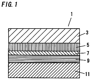
FIG. 1 are views showing an embodiment 1 of the invention, in which (a) is a cross-sectional view showing the structure of a translucent substrate (substrate for an electronic device) and (b) is a cross-sectional view showing the structure of an organic LED element.
FIG. 2 is a schematic view showing a coated state of glass particles which constitute a scattering layer of the translucent substrate according to the embodiment 1 of the invention.
FIG. 3 is a schematic view showing a fired state of glass particles which constitute a scattering layer of the translucent substrate according to the embodiment 1 of the invention.
FIG. 4 is a schematic view showing a state of the scattering layer fired at a temperature lower than the softening temperature of glass as an example for comparison with the invention.
FIG. 5 is a schematic view showing a state of the scattering layer (when fired at a temperature sufficiently higher than the softening point of the glass) according to the embodiment 1 of the invention.
FIG. 6 is a schematic view showing a state of surface waviness of the scattering layer according to embodiment 1 of the invention.
FIG. 7 is a schematic view showing a microscopic concave portion of the scattering layer surface.
FIG. 8 is a schematic view showing another microscopic concave portion of the scattering layer surface.
FIG. 9 is a schematic view showing a surface state of the scattering layer according to embodiment 1 of the present invention.
FIG. 10 is a schematic view showing a surface state of the scattering layer in Comparative Example (when the firing temperature is too high).
FIG. 11 is a graph showing a relationship between light-extraction efficiency (%) and scattering material content (vol %).
FIG. 12 is a graph showing a relationship between light-extraction efficiency (%) and refractive index of scattering materials.
FIG. 13 is a graph showing a relationship between light-extraction efficiency (%) and scattering material content (vol %).
FIG. 14 is a graph showing a relationship between light-extraction efficiency (%) and number of scattering material particles (particles/mm.sup.2).
FIG. 15 is a graph showing a relationship between light-extraction efficiency (%) and transmittance of a base material of the scattering layer (@ 1 mmt %).
FIG. 16 is a graph showing a relationship between light-extraction efficiency (%) and reflectivity (%) of a cathode.
FIG. 17 is a graph showing a relationship between proportion of light exiting to the scattering layer and refractive index of a base material of the scattering layer.
FIG. 18 is a graph showing a relationship between wavelength and refractive index of a base material of the scattering layer.
FIG. 19 is a simulation results of a relationship between wavelength and luminance on a light-receiving surface.
FIG. 20 is a flow chart illustrating a process of making a substrate according to the invention which is intended for use in an organic LED element.
FIG. 21 is a flow chart illustrating a process of fabricating an organic LED element according to the invention.
FIG. 22 is a schematic cross-sectional diagram showing a structure of an organic LED display unit.
FIG. 23 is a cross-sectional diagram showing another structure of an organic LED element according to the invention.
FIG. 24 shows results of observations from the front under conditions of Case 1 and Case 2.
FIG. 25 is a cross-sectional diagram showing a structure of an evaluation element, which appears if the element is cut along the A-A line and viewed from the direction C as shown in FIG. 26.
FIG. 26 is a top view of the evaluation element under observation from the direction B in FIG. 25.
FIG. 27 are graphs showing waviness of scattering layer surfaces, in which (A) is a graph showing waviness of the surface of a 60 .mu.m-thick scattering layer and (B) is a graph showing waviness of the surface of a 60 .mu.m-thick scattering layer prepared by polishing the scattering layer having a thickness of 20 .mu.m.
FIG. 28 is a graph showing the result of measuring the surface profile of a scattering layer by a surface roughness tester.
FIG. 29 are graphs showing results of measuring local roughness of scattering layer surfaces, in which (A) shows the measurement result of the unpolished scattering layer surface and (B) shows the measurement result of the polished scattering layer surface.
FIG. 30 is a block diagram showing a configuration of an evaluation system for evaluating light emission characteristics.
FIG. 31 is a block diagram showing measuring points.
FIG. 32 is a graph showing distribution of luminance in a central light-emission range 2210 and a peripheral light-emission range 2220.
FIG. 33 is a graph showing the average of frontal luminance values at 5 measuring points in each of individual cases where the scattering layers are different in thickness.
FIG. 34 is a graph showing luminance after correcting each 5-point average value for the quantity of light measured in the peripheral light-emission range in each of individual cases where the scattering layers are different in thickness.
FIG. 35 is a graph showing a ratio between frontal luminance in the part having no scattering layer and that in the part having a scattering layer of each evaluation element.
FIG. 36 is a graph showing results of measuring fluorescence spectra in the part having a scattering layer and in the part having no scattering layer.
FIG. 37 is a graph obtained by doubling the intensity of the fluorescence spectrum in the part having no scattering layer and overwriting the fluorescence spectrum in the part having a scattering layer with the spectrum doubled in intensity.
FIG. 38 is a graph showing results of measuring direction dependency of luminous intensity.
FIG. 39 is a graph obtained by normalizing the data shown in FIG. 38 with the front luminous intensity.
FIG. 40 is a graph showing a diameter distribution of pores.
FIG. 41 is a graph illustrating comparison of the measurement result obtained this time with the relationship of light-extraction efficiency to the number of pores (scattering materials) per mm.sup.2 in a case where the pore diameter is 2 .mu.m.
FIG. 42 is a graph showing refractive indexes of glass, ITO film and Alq.sub.3 film used for the scattering layers in evaluation experiments.
FIG. 43 is a diagram showing results of determining the relationship of surface roughness to firing temperature of the scattering layer of the translucent substrate in Example 2 of the invention.
FIG. 44 is a diagram showing results of determining the relationship of refractive index to firing temperature of the scattering layer of the translucent substrate made in Example 2 of the invention.
FIG. 45 is a diagram showing the state of light emission from the organic LED element formed using the translucent substrate made in Example 2 of the invention.
FIG. 46 is a diagram showing the state of light emission from the organic LED element formed using the translucent substrate made in Comparative Example.
FIG. 47 is a diagram showing voltage-current characteristics of the organic LED elements in Example 2 of the invention and Comparative Example.
FIG. 48 is a diagram showing current-luminance characteristics of the organic LED elements in Example 2 of the invention and Comparative Example.
FIG. 49 is a diagram showing a measuring apparatus used for measuring angular dependences of luminance and color of emission light in Example 3 of the invention.
FIG. 50 is a diagram showing spectral data on angular dependences of luminance and color of emission light from the organic LED element in Comparative Example.
FIG. 51 is another diagram showing spectral data on the angular dependences of luminance and color of emission light from the organic LED element in Comparative Example.
FIG. 52 is a diagram showing spectral data on angular dependences of luminance and color of emission light from one of the organic LED elements in Example 3 of the invention.
FIG. 53 is another diagram showing spectral data on the angular dependences of luminance and color of emission light from the organic LED element in Example 3 of the invention.
FIG. 54 is a diagram showing the chromatic coordinates of angular dependences of luminance and color of emission light from the organic LED element in Example 3 of the invention.
FIG. 55 is a diagram showing the relationship of the number of pores to the depth in the scattering layer of each of the two organic LED elements in Example 3 of the invention.
FIG. 56 is a diagram illustrating a method for measuring the transmittance of each scattering layer in Example 4 of the invention.
FIG. 57 is a diagram showing the result of determining the relationship between total light transmittance to thickness of each scattering layer in Example 4 of the invention.
FIG. 58 is a diagram showing a relationship of Haze value to thickness of each scattering layer in Example 4 of the invention.
FIG. 59 is a diagram showing the relationship between total light transmittance in Example 4 of the invention and ratio of light-extraction efficiency in Example 4 of the invention to that in the case of forming no scattering layer (light-extraction magnification).
FIG. 60 is a diagram showing the relationship between Haze value in Example 4 of the invention and ratio of light-extraction efficiency in Example 4 of the invention to that in the case of forming no scattering layer (light-extraction magnification).
Mode for carrying out the invention
Embodiment 1
A substrate for an electronic device (translucent substrate with an electrode) and an organic LED element according to an embodiment 1 of the invention are illustrated below by use of drawings. FIG. 1(a) is a diagram of a substrate for electronic device according to an embodiment 1 of the invention, and FIG. 1(b) is a cross-sectional diagram showing a structure of an organic LED element having this substrate for electronic device.
The present substrate for an electronic device, notably for use in fabricating an organic LED element, is characterized, as shown in FIG. 1(a), in that the substrate is provided with a glass substrate 101 and a scattering layer 102 as a glass layer formed on the surface 101a on a first main surface side of the glass substrate 101, the scattering layer 102 has a second surface 102b adjoining the surface 101a on the first main surface side and a first surface 102a opposite to the second surface 102b, and the first surface 102a forms waviness made up of curved faces and acts as the first main surface. Although a translucent electrode 103 is formed on the first surface 102a, FIG. 1(a) shows a state before forming the electrode. In addition, it is desirable for this surface to satisfy conditions that the waviness has a wavelength R.lamda. of a greater than 50 .mu.m and the ratio Ra/R.lamda.a of surface roughness Ra of the surface which forms waviness to the wavelength R.lamda.a of the surface waviness is from 1.0.times.10.sup.-4 to 3.0.times.10.sup.-2. The symbol 101b refers to the second main surface.
When R.lamda.a is great or waviness roughness Ra is small to such an extent that Ra/R.lamda.a is below 1.0.times.10.sup.-4, it is impossible to significantly reduce a specular reflection property. On the other hand, when waviness roughness is great to such an extent that this ratio (Ra/R.lamda.a) is beyond 3.0.times.10.sup.-2, an organic layer cannot have the form of uniform film, and it becomes difficult to make a device.
In addition, it is preferable that the surface roughness Ra of the surface which forms waviness is 30 nm or below.
An organic LED element according to the invention is made up of an electrode-attached translucent substrate 100 which has waviness, an organic layer 110 and a reflective electrode 120. The electrode-attached translucent substrate 100 includes a substrate 101 made of a translucent glass substrate, a scattering layer 102 and a translucent electrode 103.
The electrode-attached translucent substrate 100 for use in the invention is equipped with a translucent glass substrate 101, a scattering layer 102 which includes glass and is formed on the glass substrate, and a translucent electrode 103. And the scattering layer contains a base material having a first refractive index for one of wavelengths of transmitted light and a plurality of scattering materials 104 being dispersed in the base material and having a second refractive index different from the refractive index of the base material, and distribution of the scattering materials in the scattering layer diminishes from the inside of the scattering layer toward the translucent electrode. This translucent electrode 103 has a third refractive index equal to or lower than the first refractive index.
Further, the density .rho..sub.1 of the scattering materials at the position of half the thickness (.delta./2) of the scattering layer 102 made from glass and the density .rho..sub.2 of the scattering materials at a distance x (.delta./2<x.ltoreq..delta.) from the scattering layer surface on the side opposite to the translucent electrode (namely the surface on the substrate side) satisfy .rho..sub.1.gtoreq..rho..sub.2.
Furthermore, the density .rho..sub.3 of the scattering materials at a distance x (x.ltoreq.0.2 .mu.m) from a surface of the translucent electrode side of the scattering layer made from glass and the density .rho..sub.4 of the scattering materials at the distance x=2 .mu.m satisfy .rho..sub.4>.rho..sub.3. This relation, though described below, is evident from FIG. 55. Additionally, FIG. 55 shows the cases of adopting firing temperatures of 570.degree. C. and 580.degree. C., and even when the firing temperature is changed a little, similar results can be obtained.
In addition, the density .rho..sub.3 of the scattering materials at a distance x (x.ltoreq.0.2 .mu.m) from the surface of the translucent electrode side of the scattering layer made from glass and the density .rho..sub.5 of the scattering materials at the distance x=5 .mu.m satisfy .rho..sub.5>.rho..sub.3. This relation also, though described below, is evident from FIG. 55.
According to this constitution, the probability that pores, crystals made to separate out or/and the scattering materials made of materials differing from the base material in composition will be present on or directly underneath the surface of the scattering layer including the glass layer is adjusted to become lower than the probability that they will be present in the interior of the scattering layer, and thereby a smooth surface can be obtained. Because of this adjustment, in the case of forming e.g. an organic LED element, the surface of the translucent substrate, or the scattering layer surface, is smooth, whereby the surface of a translucent electrode (first electrode) formed on the scattering layer can be made smooth and, when a layer having e.g. a function of emitting light is formed on the translucent electrode by a coating method, formation of a uniform layer having a function of emitting light becomes possible too, and further the inter-electrode distance between the translucent electrode and the surface of a reflective electrode (second electrode) formed on the layer having a function of emitting light can be made uniform too. As a result, localized application of a large voltage to the layer having a function of emitting light can be avoided and a long life can be ensured. Additionally, in the case of forming a display device made up of fine picture elements, such as a high-resolution display, it is required to form a pattern of fine picture elements, and therefore surface roughness not only becomes causes of variations in positions and sizes of the picture elements but also produces a problem of developing a short circuit in the organic LED element. However, the present constitution allows fine patterns to be formed with high precision.
The scattering layer, though formed directly on the glass substrate, may also be formed over the glass substrate via a barrier layer e.g. by forming a silica thin film on the glass substrate by use of a sputtering method and then forming the scattering layer. However, by forming the scattering layer made from glass on the glass substrate without interposing an adhesive or an organic layer, a very stable and flat surface can be obtained, and besides, by constructing an optical device only from inorganic substances, it becomes possible to ensure thermal stability and a long life for the device.
Characteristics of such a translucent substrate are illustrated in detail.
A schematic diagram of a state which glass powder coated by an appropriate method is in when the glass powder undergoes firing is shown in FIG. 2. This diagram illustrates a cross-section of the topmost part of a glass layer as the scattering layer included in the present translucent substrate. Such a state is brought about by dispersing glass particles G into a solvent or a solvent-resin mixture and coating the dispersion in a desired thickness. As to the particle size, for instance, glass particles measuring about 0.1 .mu.m to about 10 .mu.m in the maximum length are used. When the resin-solvent mixture is used, the resin film into which the glass particles G are dispersed is heated to decompose the resin, and thereby the state shown in FIG. 2 is developed. While FIG. 2 is a diagram drawn with brevity, gaps among glass particles are left therein.
If the glass particles G have a particle size distribution, they are supposed to have a structure that small particles enter into gaps among large particles. In the course of further raising the temperature, glass particles begin to fuse together at a temperature lower than the softening temperature of the glass by 10.degree. C. to 20.degree. C. The state of such fusion is shown in FIG. 3. When glass particles fuse together, the gaps created among glass particles as shown in FIG. 2 are deformed by softening of the glass and closed spaces are formed in the glass. The glass particles fused together at the uppermost layers thereof and form the outermost surface of the scattering layer 102 (glass layer). In the outermost surface 200, gaps forming no closed spaces are present in the form of concaves.
With a still further rise in temperature, softening and fluidization of glass progress, and the gaps inside the glass comes to form spherical pores. In the outermost surface 200 of the glass, the concaves traceable to gaps among glass particles G come to be smoothed. This state is drawn in FIG. 4. Not only pores are formed from gaps among glass particles G, but also there is a case where gas is produced during the glass softening and forms pores. For instance, there may also be a case where organic matter stuck to the glass layer surface evolves CO.sub.2 by undergoing decomposition and forms pores. Likewise, a substance decomposable by heat is introduced, and thereby evolution of pores may be positively aimed at. The state like this can be generally attained in the vicinity of the softening temperature. Because glass has a high viscosity of 10.sup.7.6 poise at the softening temperature, pores having a size of several micrometers or below cannot float up. Thus it is possible to further smooth the surface while inhibiting pores from floating up by not only adjusting the composition of substances to evolve small pores but also further raising the temperature or prolong a retention time. By cooling the surface in a state of being smoothed in such a manner, it becomes possible to provide the glass scattering layer as shown in FIG. 5 which has a smooth surface and contains scattering materials at a lower density in the surface area than in the interior of the glass layer.
By controlling the composition of substances and the firing temperature for forming the glass layer in such a manner, it is possible to prevent pores and concaves from being made in the outermost surface of the glass layer while leaving pores inside the glass layer. In other words, it becomes possible to provide an electrode-attached translucent substrate having excellent scattering characteristics and high surface smoothness by adjusting both a firing temperature profile and a firing time so that the scattering materials are prevent from moving upward and remain inside the glass layer without going up to the surface.
At this time, the outermost surface of the glass layer forms curves with waviness. A schematic diagram thereof is shown in FIG. 6. The term "waviness" used herein refers to the waviness having a period R.lamda.a of 10 .mu.m or longer. The magnitude of the waviness (roughness) is of the order of 0.01 .mu.m to 5 .mu.m. Even when such waviness is present, microscopic smoothness is retained. As far as the conditions of R.lamda.a>10 .mu.m and Ra/R.lamda.a=1.0.times.10.sup.-5 to 1.0.times.10.sup.-1 are satisfied, reflections in the reflective electrode can be practically reduced, and therefore it is appropriate that R.lamda.a be greater than 10 .mu.m and Ra/R.lamda.a be from 1.0.times.10.sup.-5 to 1.0.times.10.sup.-1. If further desired, it is still better that R.lamda.a is greater than 50 .mu.m and Ra/R.lamda.a be from 1.0.times.10.sup.-4 to 3.0.times.10.sup.-2.
For formation of such waviness, it is required to select a processing temperature, a glass material for the glass layer, size of glass particles, a substrate material and so on. In the case where the processing temperature is low, though there is a case where microscopic concaves in the outermost surface remain, the shape of concaves can be changed from an overhanging shape as shown in FIG. 7 to a gentle shape as shown in FIG. 8 by prolonging the firing time. The term "overhanging" used here means that, as shown in FIG. 7, .theta. takes on an acute angle, while the term gentle means that, as shown in FIG. 8, .theta. takes on an obtuse angle or a right angle. When the shape of concaves is gentle, it can be said that the concaves have a low possibility of causing an inter-electrode short cut in an organic LED element. It is preferable that the firing temperature is higher than the glass transition temperature by about 40.degree. C. to about 100.degree. C. In a case of amorphous glass in particular, it is preferable that such a temperature different is on the order of 40.degree. C. to 60.degree. C. When the firing temperature is too low, firing becomes insufficient and smoothing of the surface is not attained. Therefore it is more preferable that the firing temperature is higher than the glass transition temperature by about 50.degree. C. to about 60.degree. C.
Further, in a case where an organic LED element formed as the upper layer of a scattering layer has a reflective electrode, formation of waviness made up of curved faces on the surface of the scattering layer allows prevention of degradation in appearance of the element by a reflection in the reflective electrode. When a reflective electrode was used, reflections in the reflective electrode used to appear under no emission of light, there used to be a problem of marring the appearance of the element. However, the waviness formed on the scattering layer surface allows elimination of such a reflection and maintenance of the beauty of the element under no emission of light.
In addition, by optimizing conditions of formation of the scattering layer, the invention causes neither reduction in accuracy of patterns formed as an upper layer of the substrate nor variations in the inter-electrode distance, and besides, because the invention makes it possible to enlarge an area of contact between the electrode and a layer having a function of emitting light, an effective element area can be enlarged and an organic LED element having a long life and a high luminance can be formed.
Furthermore, the surface roughness Ra of the scattering layer surface is preferably 30 nm or below. And it is more preferred that the surface roughness of the scattering layer be 10 nm or below.
The description continues in the full USPTO document.
 Lapsed, fee not paid23 drawings

