Background of the invention
1. Field of the invention
The present invention relates to an image forming apparatus for forming images, and more particularly, to an image forming apparatus using an electrophotographic process.
2. Description of the related art
In a printing apparatus for printing images by an electrophotographic process, a surface of a drum-type electrophotographic photosensitive member (hereinafter, referred to as photosensitive drum) is uniformly charged to a predetermined potential by a charging unit. In the charging unit, corona charging which is non-contact charging is generally performed. In the corona charging, a high voltage is applied to a thin corona discharge wire to generate corona, and the corona acts on the surface of the photosensitive drum which is to be charged.
In recent years, a contact charging process which is advantageous in terms of a low-voltage process, a low ozone generation amount, and a low cost is becoming mainstream. The contact charging process is a process for bringing, for example, a roller charging member (hereinafter, referred to as charging roller) into contact with the surface of the photosensitive drum and applying a voltage to the charging roller to charge the photosensitive drum. The voltage applied to the charging roller may be only a DC voltage. However, when an AC voltage is applied to alternately generate positive discharging and negative discharging, more uniform charging may be achieved. For example, it is known that an AC voltage having a peak-to-peak voltage (Vpp) which is twice or more larger than a threshold voltage (charge start voltage), at which discharging to the photosensitive drum is started when a DC voltage is applied, is superimposed on the DC voltage to obtain an oscillation voltage to be applied, to thereby uniformly charge the photosensitive member.
When a sinusoidal voltage is applied to the charging roller, the voltage causes a resistive load current to flow into a resistive load between the charging roller and the photosensitive drum, a capacitive load current to flow into a capacitive load between the charging roller and the photosensitive drum, and a discharge current to flow between the charging roller and the photosensitive drum. As a result, the sum of currents flows into the charging roller. As is empirically known, a discharge current amount is desirably maintained to a value equal to or larger than a predetermined value in order to obtain stable charging. Note that, when the discharge current amount becomes equal to or larger than the predetermined value in a high-humidity environment, image defects may occur.
In recent years, high image quality and high stability have been desired, and discharge current control for controlling the discharge current amount has been proposed (see Japanese Patent Application Laid-Open No. 2001-201921).
Image forming apparatuses have been used in a wider range of environments, and increasingly used particularly in a low-temperature and low-humidity environment. In line with this trend, a reduction in cost is strongly desired, and hence the image forming apparatuses are required to be used with a low peak-to-peak voltage (Vpp).
When the discharge current control is employed in the low-temperature and low-humidity environment, a resistance of a charging device increases, and hence a necessary discharge current amount increases. In addition, it is necessary to apply a voltage for computation, and hence the main body of the printing apparatus is required to have a capacity higher than necessary. Therefore, significant power is wasted.
Summary of the invention
Therefore, the present invention provides an image forming apparatus capable of performing stable charging and thus stable image formation over a long term by changing a method of determining a voltage value applied to a charging device.
Moreover, the present invention provides an image forming apparatus capable of performing charging suitable for an environmental condition and thus performing image formation suitable for the environmental condition by changing a method of determining a voltage value applied to a charging device based on a predetermined environmental condition.
According to the present invention, an image forming apparatus includes: an image bearing member for bearing an image; a charging unit for charging the image bearing member; a first applied voltage determining unit for obtaining a relationship between a voltage applied to the charging unit and a discharge current amount and determining a voltage value of the applied voltage corresponding to a predetermined discharge current amount; a second applied voltage determining unit for determining a voltage value of a voltage to be applied to the charging unit from voltage values stored in advance in a storage unit; and a control unit for controlling the charging unit based on the voltage value determined by one of the first applied voltage determining unit and the second applied voltage determining unit.
According to the present invention, the first and second applied voltage determining units for determining the voltage values of the voltages applied to the charging unit are provided to select any one of the values, and hence an image forming apparatus which is stable over a long term and low in cost may be provided.
Further features of the present invention will become apparent from the following description of exemplary embodiments with reference to the attached drawings.
Brief description of the drawings
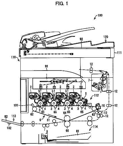
FIG. 1 is a schematic diagram illustrating a structural example of ah image forming apparatus according to an embodiment of the present invention.
FIG. 2 illustrates a schematic structural example of a charging member according to the embodiment of the present invention.
FIG. 3 is a graph illustrating an output of a Fischer scope H100V (produced by H. Fischer).
FIGS. 4A and 4B illustrate schematic structural examples of a photosensitive drum according to the embodiment of the present invention.
FIG. 5 is a graph illustrating a discharge current amount according to the embodiment of the present invention.
FIG. 6 is a graph illustrating discharge current control according to the embodiment of the present invention.
FIG. 7 is a graph illustrating a problem of the discharge current control in a low-temperature environment.
FIG. 8 is a flow chart illustrating an example of processing of the image forming apparatus according to the embodiment of the present invention.
FIG. 9 illustrates an example of an environment table, which is the basis for the processing illustrated in FIG. 8.
FIG. 10 is a flow chart illustrating another example of processing of the image forming apparatus according to the embodiment of the present invention.
FIG. 11 illustrates another example of the environment table, which is the basis for the processing illustrated in FIG. 10.
FIG. 12 is a flow chart illustrating another example of processing of the image forming apparatus according to the embodiment of the present invention.
FIG. 13 illustrates another example of the environment table, which is the basis for the processing illustrated in FIG. 10.
FIG. 14 illustrates another example of the environment table, which is the basis for the processing illustrated in FIG. 10.
FIG. 15 is a block diagram illustrating an example of constant voltage control.
FIG. 16 is a schematic view illustrating an operation portion including an input portion and a display portion.
Description of the embodiment
Hereinafter, an embodiment of the present invention is described in detail with reference to the attached drawings.
[Image Forming Apparatus]
FIG. 1 is a schematic diagram illustrating a structural example of an image forming apparatus. The image forming apparatus is an electrophotographic image forming apparatus of a contact charging type and a transfer type which uses a drum type electrophotographic photosensitive member (hereinafter, referred to as photosensitive drum) 1 as a rotatable image bearing member for forming an electrostatic latent image.
The photosensitive drum 1 is supported to be freely rotatable about a drum axis line and rotated by a driving mechanism (not shown) at a predetermined speed in a clockwise direction indicated by the arrow.
A surface of the rotated photosensitive drum 1 is uniformly charged to a predetermined potential with a predetermined polarity by a charging unit. In this example, the charging unit is a contact charging device (roller charging device) using a charging roller 2 as a charging member. The charging roller 2 is a conductive elastic roller having a roller shaft member (conductive base or cored bar). The charging roller 2 is rotatably supported by bearing members at both end portions of the roller shaft member and pressed to be in contact with the photosensitive drum 1 by a predetermined pressing force while a roller axis line is substantially parallel to the drum axis line of the photosensitive drum 1. In this example, the charging roller 2 is rotated according to the rotation of the photosensitive drum 1. Resin particles are mixed in a surface layer of the charging roller 2 to form an unevenness surface. The charging roller 2 is described later. Although not illustrated, the charging roller 2 is provided with a rotating brush (cleaning brush) as a cleaning member for cleaning the surface thereof. The rotating brush is rotated according to the rotation of the charging roller 2 to scrape off foreign matters deposited on the surface of the charging roller, to thereby prevent the surface of the charging roller from being locally or entirely contaminated with foreign matters.
A predetermined DC voltage generated by a high-voltage source 16 (DC charging type) or a voltage obtained by superimposing a predetermined AC voltage on the predetermined DC voltage (AC+DC charging type) is applied as a charge bias to the roller shaft member of the charging roller 2. Such control is performed by an engine control section 17. The manner of the control is changed based on environment information output from an environmental sensor 18. That is, the engine control section 17 serves as a first applied voltage determining unit associated with discharge current control, for obtaining a relationship between art applied voltage to the charging roller 2 and a discharge current amount and determining a voltage value of an applied voltage corresponding to a predetermined discharge current amount, and a second applied voltage determining unit associated with constant voltage control, for determining a voltage value of a voltage to be applied to the charging roller 2 based on the environment information detected by the environmental sensor 18. In such a structure, the surface of the rotated photosensitive drum 1 is uniformly contact-charged to a predetermined potential with a predetermined polarity. In this example, the surface of the photosensitive drum 1 is charged to a predetermined negative potential.
The charged surface of the photosensitive drum 1 is image-exposed by an image exposure unit 3. Therefore, a potential of an exposed bright area of the surface of the photosensitive drum is reduced to form an electrostatic latent image corresponding to an image exposure pattern on the surface of the photosensitive drum. The image exposure unit 3 may be an analog exposure apparatus for imaging and projection-exposing ah image of an original, or a digital exposure apparatus, for example, a laser scanner or an LED array. In this example, a laser scanner for laser scanning exposure L with a wavelength .lamda. of 780 mm is used as the image exposure unit 3.
The electrostatic latent image formed on the surface of the photosensitive drum as described above is developed as a toner image by a developing unit. In this example, the developing unit is a jumping reverse developing device 4 using a one-component magnetic negative chargeable toner as a developer. In the present invention, a method of using a mixture of toner particles of another developing method and magnetic carriers as a developer and carrying this developer by a magnetic force to perform development in a contact state with the photosensitive drum (two-component contact development) may be employed. Alternatively, a method of using the above-mentioned two-component developer to perform development in non-contact state with the photosensitive drum 1 (two-component non-contact development method) may be suitably employed. The developing device 4 includes a developing sleeve 5 which is rotatably driven and a hopper portion 6 for supplying a developer to the developing sleeve 5. The developing sleeve 5 and the photosensitive drum 1 are separated from each other to maintain a constant interval of 0.3 mm in a longitudinal direction of the device. The developing sleeve 5 is applied with a voltage obtained by superimposing a predetermined AG component and DC component on each other from a development bias application power supply section (not shown). Therefore, the electrostatic latent image on the surface of the photosensitive drum is subjected to jumping reverse development by the developing device 4.
A toner image formed on the surface of the photosensitive drum reaches a transferring portion T corresponding to a contact nip portion between the photosensitive drum 1 and a transferring roller 7 by the rotation of the photosensitive drum 1 and transferred to a recording material P fed to the transferring portion T. The transferring roller 7 is a conductive elastic roller having a roller shaft member (conductive base or cored bar). Both end portions of the roller shaft member are rotatably supported by bearing members. The transferring roller 7 is pressed to be in contact with the photosensitive drum 1 by a predetermined pressing force while a roller axis line is substantially parallel to the drum axis line of the photosensitive drum 1.
In this example, the transferring roller 7 is rotated according to the rotation of the photosensitive drum 1. The recording material P is fed from a sheet feeding mechanism portion (hot shown) at a predetermined control timing, introduced to the transferring portion T at a suitable timing synchronized with the image formation on the photosensitive drum 1 by a registration roller (not shown), and nipped and conveyed by the photosensitive drum 1 and the transferring roller 7. The transferring roller 7 is applied with a predetermined DC voltage of opposite polarity to the polarity of the charged toner from a transfer bias application power supply section (not shown) while the recording material P passes through the transferring portion T. In this example, the predetermined DC voltage having a positive polarity is applied. Therefore, in the transferring portion T, a rear side (a surface side opposite from a surface side facing the photosensitive drum) of the recording material P is provided with positive charges and the toner image on the surface of the photosensitive drum is sequentially and electrostatically transferred to the surface of the recording material P.
When the recording material P to which the toner image is transferred exits the transferring portion T, the recording material P is separated from the surface of the photosensitive drum 1 and introduced to a fixing device (not shown) by a conveyer belt (not shown). The fixing device is a heat fixing device including a heat roller and a pressure roller as a press-contact rotating roller pair. The recording material P introduced to the fixing device enters a fixing portion corresponding to a press-contact nip portion between the roller pair to be nipped and conveyed. Therefore, an unfixed toner image on the recording material P is fixed as a fixed image on the surface of the recording material by heat and pressure. After that, the recording material is delivered as an image formation object to the outside of the apparatus main body.
After the separation of the recording material, the surface of the photosensitive drum 1 is cleaned by removing residues such as transfer residual toners and paper dusts by a cleaning device 8. The photosensitive drum 1 with the cleaned surface is repeatedly used for image formation. In this example, the cleaning device 8 is a blade cleaning device using a chip type cleaning blade 9 as a cleaning member. The cleaning blade 9 slides on and contacts with the surface of the photosensitive drum to scrape off the residues from the surface of the photosensitive drum. The scraped-off residues 10 are contained in a recovered toner containing portion 10.
[Charging Roller]
A schematic structural example of the charging member 2 according to the embodiment of the present invention is described with reference to FIG. 2.
The charging member 2 illustrated in FIG. 2 normally has a roller shape and includes a shaft member 11, a conductive elastic layer 12 formed around the shaft member 11, a softener transfer protection layer 13 formed around the conductive elastic layer 12, a resistance adjustment layer (or dielectric layer) 14 formed around the softener transfer protection layer 13, and a protective layer 15.
The shaft member 11 is not particularly limited, and hence, for example, a cored bar which is a columnar body made of metal, or a cylindrical body which is hollow and made of metal is used. Examples of the metal material include stainless steel, aluminum, copper, and plated iron.
The conductive elastic layer 12 formed around the periphery of the shaft member 11 is not particularly limited, and there are exemplified as a material for the conductive elastic layer 12 a polyurethane foam, a polynorbornene rubber, an ethylene-propylene-diene rubber (EPDM), an acrylonitrile-butadiene rubber (NBR), a hydrogenated acrylonitrile-butadiene rubber (H-NBR), a styrene-butadiene rubber (SBR), a butadiene rubber (BR), an isoprene rubber (IR), and a natural rubber (NR). Those materials may be used alone or in combination of two or more kinds thereof. A polyol component and an isocyanate component that can be used in the production of a usual polyurethane foam are particularly preferred. Examples of the above-mentioned polyol component include a polyether polyol, a polyester polyol, and a polymer polyol. Those polyol components may be used alone or in combination of two or more kinds thereof. The above-mentioned isocyanate component is not particularly limited as long as the component is a di- or more functional polyisocyanate, and examples thereof include 2,4-(or 2,6-)tolylene diisocyanate (TDI), ortho-toluidine diisocyanate (TODI), naphthylene diisocyanate (NDI), xylylene diisocyanate (XDI), 4,4'-diphenylmethane diisocyanate (MDI), carbodiimide-modified MDI, polymethylene polyphenyl isocyanate, and polymeric polyisocyanate. Those isocyanate components may be used alone or in combination of two or more kinds thereof.
It should be noted that, in addition to the above-mentioned rubbers, a foaming agent, a conductive agent, a crosslinking agent, a crosslinking promoter, an oil, and the like may be incorporated into the material for the above-mentioned conductive elastic layer 12 as required.
Examples of the above-mentioned foaming agent include inorganic foaming agents and organic foaming agents. Those foaming agents may be used alone or in combination of two or more kinds thereof.
The above-mentioned conductive agent is preferably an ionic conductive agent, and examples thereof include: cationic surfactants such as quaternary ammonium salts including perchloric acid salts, chloric acid salts, fluoroboric acid salts, sulfuric acid salts, ethosulfate salts, and benzyl halide salts (such as benzyl bromide and benzyl chloride salts) of lauryl trimethyl ammonium, stearyl trimethyl ammonium, octadodecyl trimethyl ammonium, dodecyl trimethyl ammonium, hexadecyl trimethyl ammonium, and a modified fatty acid dimethylethyl ammonium salt; anionic surfactants such as an aliphatic sulfonic acid salt, a higher alcohol sulfuric acid ester salt, a higher alcohol ethylene oxide addition sulfuric acid ester salt, a higher alcohol phosphoric acid ester salt, a higher alcohol ethylene oxide addition phosphoric acid ester salt; amphoteric surfactants such as various betaines; antistatic agents such as nonionic antistatic agents including a higher alcohol ethylene oxide, a polyethylene glycol fatty acid ester, and a polyhydric alcohol fatty acid ester; electrolytes such as salts of metals belonging to Group 1 of the periodic table including Li.sup.+, Na.sup.+, and K.sup.+, i.e., for example, LiCF.sub.3SO.sub.3, NaClO.sub.4, LiAsF.sub.6, LiBF.sub.4, NaSCN, KSCN, and NaCl, and quaternary ammonium salts; salts of metals belonging to Group 2 of the periodic table including Ca.sup.2+ and Ba.sup.2+, i.e., for example, Ca(ClO.sub.4).sub.2; and conductive agents in each of which one of those antistatic agents has at least one group having an active hydrogen capable of reacting with an isocyanate, such as a hydroxyl group, a carboxyl group, or a primary or secondary amine group. Further examples of the conductive agent include complexes of the above-mentioned conductive agents and the like with: polyhydric alcohols such as 1,4-butandiol, ethylene glycol, polyethylene glycol, propylene glycol, and polyethylene glycol, and their derivatives; or monools such as, ethylene glycol monomethyl ether, and ethylene glycol monoethyl ether. One kind or two or more kinds selected from those conductive agents may be used. It should be noted that other known ionic conductive agents and the like may be used, and the conductive agent is not limited to the materials described above.
Alternatively, other conductive agents such as general electron conductive agents may be used. Examples thereof include: conductive carbon blacks such as ketjen black and acetylene black; carbon blacks for rubber, such as SAF, ISAF, HAF, FEF, GPF, SRF, FT, and MT; carbon blacks for ink, such as oxidized carbon black; pyrolytic carbon black; graphite; conductive metal oxides such as tin oxide, titanium oxide, and zinc oxide; metals such as nickel and copper; and conductive whiskers such as a carbon whisker, a graphite whisker, a titanium carbide whisker, a conductive potassium titanate whisker, a conductive barium titanate whisker, a conductive titanium oxide whisker, and a conductive zinc oxide whisker.
Examples of the above-mentioned crosslinking agent include sulfur and peroxides.
A conductivity of the conductive elastic layer is normally set in a range of approximately 10.sup.-1.OMEGA. to 10.sup.-4.OMEGA. and thus set to a value significantly lower than the conductivity of the resistance adjustment layer. A thickness of the conductive elastic layer is normally set in a range of approximately 1 mm to 10 mm, preferably in a range of approximately 2 mm to 4 mm.
It is particularly preferred that the softener transfer protection layer 13 formed around the conductive elastic layer 12 is a layer containing N-methoxymethylated nylon as a main component in order to block and prevent exudation of a softener including an oil contained in the conductive elastic layer. Herein, the meaning of "as a main component" includes a case where the whole consists only of the main component. A thickness of the softener transfer protection layer 13 is normally set in a range of 3 .mu.m to 20 .mu.m, preferably in a range of 4 .mu.m to 10 .mu.m. An electrical resistance of the softener transfer protection layer is set to approximately 10.sup.-2.OMEGA..
The N-methoxymethylated nylon (8-nylon) is not particularly limited and thus a conventionally known material is used. The softener transfer protection layer 13 contains, as a conductive agent, carbon black, for example, Ketjen black.
The resistance adjustment layer 14 formed around the softener transfer protection layer 13 is made of at least one of epichlorohydrin rubber (CHR) and acrylic rubber (ACM) and a composition containing a conductive agent as a main component. A thickness of the resistance adjustment layer 14 relates to the present invention and is required to be normally set in a range of 50 .mu.m to 400 .mu.m, more preferably in a range of 200 .mu.m to 350 .mu.m. When the thickness is smaller than 50 .mu.m, an effect of the resistance adjustment layer 14 is too small to serve as a charging roller. When the thickness is larger than 400 .mu.m, the effect of the resistance adjustment layer 14 is too large. Therefore, it is necessary to provide a voltage in a very high state, and hence it is difficult to use a normal power supply for an electrophotographic apparatus. Note that the epichlorohydrin rubber is one of a homopolymer and a copolymer which do not contain ethylene oxide as a copolymer component.
As described above, the at least one of CHR and ACM and the conductive agent are used to cover the softener transfer protection layer 13, and may cause charging unevenness but are essential to take advantage of charging characteristics. An electrical resistance of the resistance adjustment layer 14 is set in a range of 10.sup.5.OMEGA. to 10.sup.8.OMEGA..
The conductive agent may be one of an ion conductive agent and an electron conductive agent which are used for the resistance adjustment layer 14.
A blending amount of the conductive agent is preferably set in a range of 0.5 part to 5 parts relative to 100 parts by weight (hereinafter, referred to as "parts") of a rubber component comprising CHR and ACM. That is, when the composition amount of the conductive agent is smaller than 0.5 part, there is a very positive effect on unevenness. However, the electrical resistance cannot be adjusted, and hence it is necessary to apply an excessive voltage. When the composition amount exceeds 5 parts, the unevenness of the conductive agent causes the unevenness of the resistance, and hence image unevenness is likely to occur in the range set in the present invention.
Examples of appropriate composition materials for forming the resistance adjustment layer 14 include a vulcanizing agent and a filler in addition to the conductive agent. The vulcanizing agent is not particularly limited, and may include a known material, for example, thiourea, triazine, or sulfur. Examples of the filler include insulating fillers such as silica, talc, clay, and titanium oxide and are used alone or in combination. A conductive filler, for example, carbon black is likely to cause dielectric breakdown under a high-voltage environment, and hence the amount of use thereof is required to be limited to a value equal to or smaller than 10% by volume relative to the rubber component.
The protective layer 15 is formed as an outermost layer around the resistance adjustment layer 14 and may be a known layer used on the surface of the charging roller. To be specific, the protective layer 15 may be the layer containing N-methoxymethylated nylon as the main component as described above, a layer which may be made of a conventionally known resin, for example, a fluorocarbon resin, a urethane resin, or an acrylic resin, or a layer containing an isocyanate compound as a main component, or may be added with at least one of a conductivity-providing agent and at least one polymer selected from the group consisting of an acrylic fluorine-based polymer and an acrylic silicone-based polymer. When a conductive agent, for example, carbon black is mixed and dispersed in the protective layer, conductivity in a case of low-temperature and low-humidity is excellent and thus excellent performance is exhibited even in the low-temperature and low-humidity environment. A thickness of the protective layer 15 is set preferably in a range of 1 .mu.m to 25 .mu.m, more preferably in a range of 3 .mu.m to 20 .mu.m. An electrical resistance value of the protective layer 15 is set in a range of 10.sup.7 .OMEGA.cm to 10.sup.11 .OMEGA.cm. The conductive agent is not limited to carbon black and a conventionally known conductive agent may be used instead of the carbon black.
Here, examples of the isocyanate compound include 2,6-tolylene diisocyanate (TDI), 4,4'-diphenylmethane diisocyanate (MDI), para-phenylene diisocyanate (PPDI), 1,5-naphthalene diisocyanate (NDI), and 3,3-dimethyldiphenyl-4,4'-diisocyanate (TODI), and also include multimers and modified products of the isocyanate compounds described above.
In addition, the acrylic fluorine-based polymer and the acrylic silicone-based polymer are ones each of which is soluble in a given solvent and capable of reacting, with an isocyanate compound to form a chemical bond. The acrylic fluorine-based polymer is, for example, a solvent-soluble, fluorine-based polymer which has a hydroxyl group, ah alkyl group, or a carboxyl group. Examples thereof include a block copolymer of an acrylic acid ester and a fluoroalkyl acrylate, and its derivatives. In addition, the acrylic silicone-based polymer is a solvent-soluble, silicone-based polymer, and examples thereof include a block copolymer of an acrylic acid ester and an acrylic acid siloxane ester, and its derivatives.
When a conductive agent, for example, carbon black is mixed and dispersed in the protective layer 15, environmental characteristics including conductivity in a case of low-temperature and low-humidity are excellent and thus excellent performance is exhibited even in the low-temperature and low-humidity environment. A thickness of the protective layer 15 is normally set preferably in a range of 5 .mu.m to 30 .mu.m, more preferably in a range of 7 .mu.m to 23 .mu.m. An electrical resistance value of the protective layer is set in a range of 10.sup.3.OMEGA. to 10.sup.5.OMEGA.. The conductive agent is not limited to carbon black and a conventionally known conductive agent may be used instead of the carbon black.
For example, the charging roller 2 in the present invention may be produced as follows. That is, an adhesive agent is applied to an outer circumference surface of a cored bar 11 and the conductive elastic layer 12 is formed by mold vulcanization using the rubber composition described above. A mixed resin liquid in which N-methoxymethylated nylon is mixed with a conductive agent is prepared in advance. A surface of the conductive elastic layer 12 is polished if necessary, and then subjected to coating the mixed resin liquid by spraying or dipping and dried. If necessary, thermal treatment is performed for cross linking to form the softener transfer protection layer. The resistance adjustment layer 14 is formed on the softener transfer protection layer 13 containing the conductive agent. The resistance adjustment layer 14 may be formed as follows. The at least one of CHR and ACM and the ion conductive agent are kneaded with a reinforcing agent, a processing aid, a vulcanizing agent, and a filler by a normal rubber processing method (Banbury mixer or roll) to obtain an unvulcanized rubber composition. The unvulcanized rubber composition is dissolved in a suitable solvent (for example, methyl ethyl ketone or methyl isobutyl ketone), applied to an outer circumference surface of the conductive elastic layer and then dried, and vulcanized by heating. A dip method is preferred for the application. The dip method is a method of performing dipping in a dip solution and drying while a film thickness is controlled based on a drawing speed. Next, a roll on which the conductive elastic layer 12 is formed is repeatedly immersed by the dip method to form a rubber film containing the conductive agent as the main component on the outer circumference surface of the conductive elastic layer 12. In this case, it is preferred that conditions such as viscosity of the dip solution, an up-and-down speed, the number of up-and-down movements, and a dry time period be set so that a thickness of a liquid film of the solution containing the conductive agent as the main component is in a range of 50 .mu.m to 400 .mu.m when dried. The roll with the formed liquid film is dried at a temperature in a range of 25.degree. C. to 80.degree. C. for 0.5 hours to 4 hours to remove the solvent, and subsequently heated at a temperature in a range of 150.degree. C. to 200.degree. C. for 10 minutes to 2 hours to vulcanize the rubber film containing the conductive agent component as the main component, to thereby obtain the resistance adjustment layer. Next, the resistance adjustment layer 14 formed as described above is coated by spraying or dipping with a resin liquid containing fluororesin or the resin liquid mixed with a conductive agent in some cases, and then dried. If necessary, thermal treatment is performed for cross linking to form the protective layer. Therefore, the layer structure as illustrated in FIG. 2 may be obtained. The layer structure is a preferred structure, and a four or more-layer structure may be formed by repeating application and drying. A three-layer structure in which the protective layer (outermost layer) and the resistance adjustment layer are integrally formed or a two-layer structure in which the softener transfer protection layer is further integrally formed therewith may be applied. A two-layer structure may be applied in which the conductive elastic layer 12, the resistance adjustment layer 14, and the softener transfer protection layer 13 are integrally formed and coated with only the protective layer 15.
A total electrical resistance of the obtained charging roller 2 is set in a range of approximately 10.sup.3.OMEGA. to 10.sup.8.OMEGA.. As described above, the electrical resistance is largely determined based on conductive agent amounts of the resistance adjustment layer 14 and the protective layer 15. In view of film thickness, the electrical resistance is substantially determined based on the conductive agent amount of the resistance adjustment layer 14. However, the present invention is not limited to this.
The resistance value of the charging roller according to the present invention is measured as follows. The photosensitive drum of the image forming apparatus is exchanged for a drum made of aluminum. After that, a voltage of 100V is applied between the drum made of aluminum and the cored bar 11 of the charging roller 2 and a value of current flowing therebetween is measured to obtain the resistance value of the charging roller 2.
[Photosensitive Member]
Next, general matters of the image bearing member (photosensitive member) 1 according to the present invention are described below. The long life of the photosensitive member is intended. However, the present invention is not limited to this and a surface protective layer 56 may be omitted.
A feature (example) of the surface protective layer intended for the long life of the photosensitive member according to the embodiment of the present invention is briefly described first. A universal hardness value (HU) and elastic deformation ratio of the surface protective layer 56 are measured using a microhardness measuring apparatus (Fischer scope H100V produced by Fischer) in which an indentation depth with respect to a load is directly read to continuously obtain hardness while the load is continuously imposed on an indenter. The used indenter is a Vickers quadrangular pyramid diamond indenter having an opposite face angle of 136.degree.. With respect to a load condition, a final load is 6 mN. The measurement is performed stepwise at 273 points for each retaining time period of 0.1 seconds.
FIG. 3 is a schematic graph illustrating an output of the Fischer scope H100V (produced by H. Fishere). In the graph, the ordinate indicates the load (mN) and the abscissa indicates an indentation depth h (.mu.m). The graph exhibits a result obtained in a case where the load is increased stepwise to 6 mN and then reduced stepwise in the same manner. The universal hardness value (hereinafter, referred to as HU) is defined by Expression
described below based on an indentation depth obtained when the load is imposed at 6 mN. HU=(test load (N))/(surface area of Vickers indenter under test load (mm.sup.2))=0.006/26.43 h.sup.2 (N/mm.sup.2)
where h indicates an indentation depth under the test load (mm).
The elastic deformation ratio is obtained from a work (energy) of the indenter acting on a film, that is, a change in energy due to an increase or reduction in load of the indenter to the film, and calculated by the following expression. A total work Wt (nW) is expressed by an area surrounded by A-B-D-A illustrated in FIG. 3 and an elastic deformation work We (nW) is expressed by an area surrounded by C-B-D-C. (Elastic Deformation Ratio)=We/Wt.times.100(%)
As described above, an example of performance required for the organic electrophotographic photosensitive member includes improved durability with respect to mechanical degradation. It is generally expected that film hardness is high when a deformation amount which is caused by an external force is small, and thus the durability of the electrophotographic photosensitive member with respect to mechanical degradation seems to improve with an increase in pencil hardness or Vickers hardness. However, even when hardness obtained by the measurement is high, the durability is not necessarily improved.
As a result of intensive studies, the inventors of the present invention found that the surface layer of the photosensitive member is resistant to mechanical degradation in a case where the HU value and the elastic deformation ratio value are in certain ranges. That is, when a hardness test is performed using the Vickers quadrangular pyramid diamond indenter and an electrophotographic photosensitive member in which a HU in a case of indentation at a maximum load of 6 mN is equal to or larger than 150 N/mm.sup.2 and equal to or smaller than 220 N/mm.sup.2 and an elastic deformation ratio is equal to or larger than 40% and equal to or smaller than 65% is provided, the characteristic was significantly improved. In order to further improve the characteristic, the HU value is more preferably equal to or larger than 160 N/mm.sup.2 and equal to or smaller than 200 N/mm.sup.2.
The HU and the elastic deformation ratio cannot be separately considered. However, for example, in a case that the HU exceeds 220 N/mm.sup.2, when the elastic deformation ratio is smaller than 40%, an elastic force of the photosensitive member is insufficient, and when the elastic deformation ratio is larger than 65%, even if the elastic deformation ratio is large, an elastic deformation amount becomes small. As a result, a large force is locally applied, and hence a deep defect occurs because of paper dusts and toners which are caught by the cleaning blade and the charging roller. Thus, it is expected that a photosensitive member having a high HU is not necessarily optimum.
In a case where the HU is smaller than 150 N/mm.sup.2 and the elastic deformation ratio exceeds 65%, even when the elastic deformation ratio increases, a plastic deformation amount also becomes larger. Therefore, shaving or minute scratching occurs because of rubbing with paper dusts and toners which are caught by the cleaning blade and the charging roller.
Considering the long life of the photosensitive drum 1 used in the present invention, at least the surface layer of the electrophotographic photosensitive member contains a compound cured by one of polymerization and cross linking. Heat, light (visible light or ultraviolet light), and radiation may be used for a curing method.
Therefore, in this embodiment, the following method is employed as a method of forming the surface layer of the photosensitive member. A compound, which is used for the surface layer and may be cured by one of polymerization and cross linking, is melted or contained in an application solution, and the application solution is used and applied by one of a dip coating method, a spray coating method, a curtain coating method, and a spin coating method. After that, the applied compound is cured by the curing method.
The description continues in the full USPTO document.
 Lapsed, fee not paid12 drawings