Cross-reference to related application
This application claims priority to Japanese Patent Application No. 2010-073846, which was filed on Mar. 26, 2010, the contents of which are incorporated herein by reference in its entirety.
Background of the invention
1. Field of the invention
The present invention relates to a laser fixing device, an image forming apparatus equipped with the laser fixing device, and an image forming method employing the image forming apparatus.
2. Description of the related art
An electrophotographic image forming apparatus (such for example as a printer) is equipped with a fixing device for fixing an image onto a recording sheet. The fixing device causes a toner constituting a toner image formed on a recording sheet to melt, thereby fixing the toner image onto the recording sheet.
As an example of such a fixing device, there is known a fixing device of heat-roller fixing type comprising a fixing roller and a pressure section, such as described in Japanese Unexamined Patent Publication JP-A 11-38802 (1999). In this heat-roller type fixing device, a recording sheet bearing a yet-to-be-fixed toner image is sandwiched between the fixing roller having a heating portion thereinside and the pressure section which is brought into pressure-contact with the fixing roller. In this way, the toner borne on the recording sheet is fused on the recording sheet.
In such a heat-roller type fixing device, the surface temperature of the fixing roller needs to be raised to a predetermined level by the heating portion to fuse the toner under application of heat. Therefore image formation cannot be effected immediately upon start-up of the apparatus, and a certain amount of time is required to be ready for image formation. Furthermore, when it is desired to keep the surface of the fixing roller at a predetermined temperature for immediate image formation, the surface of the fixing roller needs to be heated continuously, which results in an increase in energy consumption.
In view of the foregoing, as a fixing device capable of fixing toner images without spending much time while suppressing an increase in energy consumption, there is proposed an optical fixing device for fusing and fixing a toner by exploiting optical energy.
In Japanese Unexamined Patent Publication JP-A 7-191560 (1995), as an optical fixing device, there is shown a laser fixing device having an array of a plurality of laser light emitting devices for applying laser light to a toner. According to the laser fixing device described in JP-A 7-191560, in contrast to a laser fixing device having a single laser light emitting device only, there is no need to cause laser light reflection by means of a polygon mirror or otherwise. It will thus be seen that the laser fixing device can be made compact.
In addition, in Japanese Unexamined Patent Publication JP-A 2005-115194, as an optical fixing device, there is shown a flash fixing device for fusing a toner by means of flash light having wavelengths ranging from 800 nm to 1000 nm. In JP-A 2005-115194, as a light fixable toner, there is shown an infrared-fixable toner containing an infrared absorbing agent having an absorption peak wavelength within a range of from 800 nm to 1000 nm in terms of light absorption characteristics.
Examples of the light fixable toner includes, in addition to the infrared-fixable toner, a visible light-fixable toner configured to be fused and fixed by visible light and an ultraviolet-fixable toner configured to be fused and fixed by ultraviolet light. These light fixable toners differ from one another not only in light absorption characteristic but also in the quality of obtained images. For example, given that an image is formed by using the infrared-fixable toner, since the infrared absorbing agent even absorbs visible light in a range near the infrared region, it follows that the obtained image suffers a decline in color reproducibility in its red-color area. It is therefore desirable to select a light fixable toner for use appropriately according to purposes.
What must be necessary for appropriate use of a light fixable toner as the situation demands is an optical fixing device and an image forming apparatus as well adapted to use of a plurality of types of light fixable toners having different light absorption characteristics. In this respect, there is a problem in the optical fixing devices disclosed in JP-A 7-191560 and JP-A 2005-115194 in that these optical fixing devices are designed to deal with only one light fixable toner.
Summary of the invention
The invention has been devised to overcome the problem as mentioned supra, and accordingly its object is to provide a laser fixing device adapted to use of two types of light fixable toners having different light absorption characteristics, an image forming apparatus equipped with the laser fixing device, and an image forming method employing the image forming apparatus.
The invention provides a laser fixing device adapted to use of two types of light fixable toners having different light absorption characteristics, comprising:
a laser light emitting section for emitting laser light; and
a wavelength conversion section for emitting outgoing light having a wavelength different from the one that incident laser light has,
the laser light being applied to one of the two light fixable toners and the outgoing light which is emitted from the wavelength conversion section being applied to the other toner.
According to the invention, two types of light having different wavelengths can be applied to their respective light fixable toners by the laser light emitting section and the wavelength conversion section. This makes it possible to provide a laser fixing device capable of fusing and fixing two types of light fixable toners having different light absorption characteristics.
Moreover, it is preferable that the laser light emitting section is configured to emit an infrared ray as the laser light.
According to the invention, at least an infrared-fixable toner can be fused and fixed through irradiation of an infrared ray effected by the laser light emitting section.
Moreover, it is preferable that the wavelength conversion section is configured to emit an ultraviolet ray as the outgoing light emitted from the wavelength conversion section.
According to the invention, at least an ultraviolet-fixable toner can be fused and fixed through irradiation of an ultraviolet ray emitted from the wavelength conversion section.
Moreover, it is preferable that the wavelength conversion section is an SHG element employing quasi phase matching.
According to the invention, an ultraviolet ray can be emitted by the SHG element employing quasi phase matching.
Moreover, it is preferable that the laser fixing device further comprises a conveying section for conveying a recording medium to a location which is irradiated with the laser light and the outgoing light emitted from the wavelength conversion section, and
the conveying section exhibits, at least at its part irradiated with the laser light and the outgoing light emitted from the wavelength conversion section, an infrared transmittance of greater than or equal to 70% and an ultraviolet transmittance of greater than or equal to 80%.
According to the invention, that part of the conveying section which is irradiated with light exhibits an infrared transmittance of greater than or equal to 70% and an ultraviolet transmittance of greater than or equal to 80%. Accordingly, the conveying section is resistant to light-induced quality degradation even under application of both an infrared ray and an ultraviolet ray, and can thus be used for a longer period of time.
Moreover, the invention further provides an electrophotographic image forming apparatus configured so that a light fixable toner is fixed onto a recording medium by the laser fixing device mentioned above.
According to the invention, there is provided an image forming apparatus which is adapted to use of two types of light fixable toners having different light absorption characteristics with the provision of the laser fixing device.
Moreover, the invention further provides an image forming method for forming an image by using the image forming apparatus mentioned above and a light fixable toner containing a light absorbing material which absorbs light emitted from the laser fixing device mentioned above, comprising:
a development step of forming a light fixable toner image on an image bearing member disposed in the image forming apparatus by a developing device disposed in the image forming apparatus;
a transfer step of transferring the light fixable toner image formed in the development step onto a recording medium by a transfer section disposed in the image forming apparatus; and
a fixing step of fusing and fixing the light fixable toner constituting the light fixable toner image on the recording medium by applying at least one of the laser light and outgoing light emitted from the wavelength conversion section to the light fixable toner image borne on the recording medium by means of the laser fixing device.
According to the invention, there is provided an image forming method which is adapted to use of two types of light fixable toners having different light absorption characteristics with the provision of the fixing step of fixing the light fixable toner by using the laser fixing device.
Moreover, it is preferable that the light absorbing material is one or two or more of those selected from among polyimide, polyethylene sulfide, polyethylene naphthalate, polymethyl methacrylate, and polycarbonate.
According to the invention, the light absorbing material is one or two or more of those selected from among polyimide, polyethylene sulfide, polyethylene naphthalate, polymethyl methacrylate, and polycarbonate. Accordingly, where at least one of the laser light and the outgoing light is a near-ultraviolet ray, it is possible to obtain an image which exhibits high fixation strength.
Moreover, it is preferable that the light absorbing material is a resin material having an ultraviolet absorbing group.
According to the invention, the light absorbing material is a resin material having an ultraviolet absorbing group. Accordingly, where at least one of the laser light and the outgoing light is a near-ultraviolet ray, it is possible to obtain an image which exhibits high fixation strength.
Moreover, it is preferable that, when an image is formed by putting a light fixable toner of black color and a light fixable toner of another color on top of each other, in the transfer step, transfer is so performed that the light fixable toner of another color is overlaid upstream of the light fixable toner of black color in a direction of light irradiation set for the fixing step.
According to the invention, in the transfer step, transfer is so performed that the light fixable toner of a color other than black is overlaid upstream of the light fixable toner of black color in the direction of light irradiation. This makes it possible to apply light which is relatively high in intensity to the light fixable toner of a color other than black having a relatively low light absorption efficiency, and therefore it is possible to fix the light fixable toner of a color other than black properly. Since the light fixable toner of black color has a relatively high light absorption efficiency, even if light applied thereto is relatively low in intensity, it is possible to fix the light fixable toner of black color properly.
Brief description of the drawings
Other and further objects, features, and advantages of the invention will be more explicit from the following detailed description taken with reference to the drawings wherein:
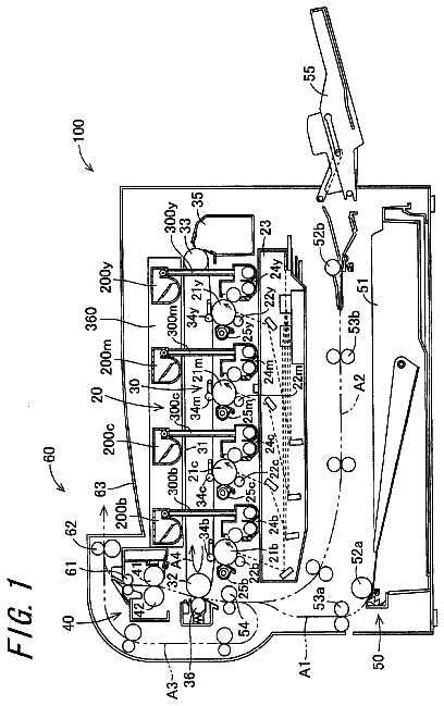
FIG. 1 is a schematic view showing the structure of an image forming apparatus;
FIG. 2 is a schematic view showing the structure of a developing device provided in the image forming apparatus;
FIG. 3 is a partially cutaway schematic view of a laser fixing device;
FIG. 4 is a sectional view of the laser fixing device taken along the line A-A of FIG. 3;
FIGS. 5A and 5B are schematic views showing a laser fixing device;
FIG. 6 is a view showing the light transmittance of polyimide; and
FIG. 7 is a flowchart for explaining an image forming method according to the invention.
Detailed description
Now referring to the drawings, preferred embodiments of the invention will be described in detail.
To begin with, an image forming apparatus 1000 equipped with a laser fixing device 100 according to a first embodiment of the invention will be described. FIG. 1 is a schematic view showing the structure of the image forming apparatus 1000. FIG. 2 is a schematic view showing the structure of a developing device 24 provided in the image forming apparatus 1000. The image forming apparatus 1000, which is built as a multi-functional peripheral having a copier function, a printer function, and a facsimile function, acts to form a full-color or monochromatic image on a recording medium in response to image information transmitted thereto. That is, the image forming apparatus 1000 has three printing modes, namely a copier mode (duplicator mode), a printer mode, and a facsimile mode. In this construction, for example, in response to operation input from an operating section (not shown) and receipt of a print job from a personal computer, a portable terminal unit, an information recording/storage medium, and external equipment using a memory device, a printing mode is selected by a control unit section (not shown).
The image forming apparatus 1000 includes a toner image forming section 20, a transfer section 30, the laser fixing device 100, a recording medium supply section 5, a discharge section 60, and the control unit section (not shown). The toner image forming section 20 includes photoreceptor drums 21k, 21c, 21m, and 21y, charging sections 22k, 22c, 22m, and 22y, an exposure unit 23, developing devices 24k, 24c, 24m, and 24y, and cleaning units 25k, 25c, 25m, and 25y. The transfer section 30 includes an intermediate transfer belt 31, a driving roller 32, a driven roller 33, intermediate transfer rollers 34k, 34c, 34m, and 34y, a transfer belt cleaning unit 35, and a transfer roller 36.
In order to deal with pieces of image information on different colors, namely black (k), cyan (c), magenta (m), and yellow (y) included in color image information on an individual basis, the photoreceptor drum 21, the charging section 22, the developing device 24, the cleaning unit 25, and the intermediate transfer roller 34 are each correspondingly four in number. In this specification, as to the four members of one kind provided for adaptability to different colors, collectively, they are designated only by the same general reference numeral, but, when distinctions are drawn among these members according to their respective colors, they are designated by the general reference numeral with the alphabetical suffix indicative of specific color.
The photoreceptor drum 21 is an image bearing member comprising a conductive substrate and a photosensitive layer (not shown) formed on the surface of the conductive substrate. The conductive substrate is, for example, a cylindrical or columnar member which is supported so as to be rotatable about its axis by a driving portion (not shown). The photosensitive layer is a member which exhibits electrical conductivity under irradiation of light. For example, the photosensitive layer is composed of a charge generating layer containing a charge generating substance and a charge transporting layer containing a charge transporting substance which are stacked on top of each other. On the surface of the photosensitive layer is formed an electric image called an electrostatic latent image through a charging process by the charging section 22 and an exposure process by the exposure unit 23. The electrostatic latent image formed on the surface of the photosensitive layer is developed by the developing device 24, whereby a toner image is formed on the surface of the photosensitive layer.
The charging section 22 is a charging device for charging the surface of the photoreceptor drum 21 to a predetermined potential with a predetermined polarity. The charging section 22 is disposed at a position facing the photoreceptor drum 21 so as to extend along a longitudinal direction of the photoreceptor drum 21. The charging section 22 is placed in contact with the surface of the photoreceptor drum 21 when a contact charging system is adopted, and yet is placed away from the surface of the photoreceptor drum 21 when a non-contact charging system is adopted.
The charging section 22 is, along with the developing device 24 and the cleaning unit 25, disposed around the photoreceptor drum 21. The charging section 22, the developing device 24, and the cleaning unit 25 are arranged around the photoreceptor drum 21 in the order named along the direction of rotation of the photoreceptor drum 21. The charging section 22 is placed vertically below the developing device 24 and the cleaning unit 25. It is preferable that the charging section 22 lies closer to the photoreceptor drum 21, compared with the developing device 24 as well as the cleaning unit 25. This makes it possible to prevent occurrence of a charging failure on the photoreceptor drum 21 without fail.
As the charging section 22, a charging device of brush type, a charging device of roller type, a corona discharge device, an ion production device, or the like can be used. The brush-type charging device and the roller-type charging device are each a charging device adapted for the contact charging system. Some brush-type charging devices employ a charging brush, and others employ a magnetic brush, for example. The corona discharge device and the ion production device are each a charging device adapted for the non-contact charging system. Some corona discharge devices employ a wire-type discharge electrode, others employ a pin array-type discharge electrode, and still others employ a stylus-type electrode, for example.
The exposure unit 23 is a unit for irradiating the surfaces of the photoreceptor drums 21k, 21c, 21m, and 21y in a charged state with light corresponding to image information of different colors, respectively, to form electrostatic latent images corresponding to the image information of the respective colors on the surfaces of the photoreceptor drums 21k, 21c, 21m, and 21y. The exposure unit 23 is so placed that light emitted therefrom passes through a region between the charging section 22 and the developing device 24 to be shone on the surface of the photoreceptor drum 21. As the exposure unit 23, for example, a laser scanning unit (LSU) having a laser light emission device and a plurality of reflection mirrors can be used. It is also possible to use a unit constructed by combining an LED (Light Emitting Diode) array, a liquid crystal shutter, and a light source properly as the exposure unit 23.
The developing device 24 includes a developer tank 241 and a toner hopper 242. The developer tank 241 accommodates a developer containing a toner which is fixable onto a recording medium through light irradiation (light fixable toner) in its internal space. The light fixable toner will be explained later on. Within the developer tank 241, a developing roller 243, a first conveyor screw 244, and a second conveyor screw 245 are rotatably supported. The developer tank 241 has an opening formed on its side surface opposed to the photoreceptor drum 21. The developing roller 243 is placed in the position of the opening through the photoreceptor drum 21.
The developing roller 243 is a member for supplying the toner to the surface of the photoreceptor drum 21 at a location in the closest proximity to the photoreceptor drum 21. In supplying a toner, on the surface of the developing roller 243 is applied a voltage of a polarity reverse to the polarity of the charge on the toner (development bias). In this way, the toner on the surface of the developing roller 243 is fed to the photoreceptor drum 21 smoothly. It is noted that, by making a change to the value of the development bias, it is possible to control the amount of toner to be fed to the photoreceptor drum 21 (toner attachment amount).
The first conveyor screw 244 is a member placed facing the developing roller 243, for supplying a toner around the developing roller 243. The second conveyor screw 245 is a member placed facing the first conveyor screw 244, for supplying a toner which has just been newly fed into the developer tank 241 from the toner hopper 242, around the first conveyor screw 244. The toner hopper 242 is so disposed that a toner replenishment port (not shown), which is created in a lower part thereof in a vertical direction, communicates with a toner reception port (not shown) created in an upper part of the developer tank 241 in the vertical direction. The toner hopper 242 supplies the toner that it receives from a toner cartridge (not shown) attached to the image forming apparatus 1000 interiorly thereof to the developer tank 241 according to the condition of developer consumption.
The cleaning unit 25 removes, after a toner image has been transferred from the photoreceptor drum 21 to the intermediate transfer belt 31, the toner remaining on the surface of the photoreceptor drum 21 and cleans the surface of the photoreceptor drum 21. For example, the cleaning unit 25 includes a platy member which is abutted against the photoreceptor drum 21 and a container-like member for collecting the removed toner.
According to the toner image forming section 20, the surface of the photoreceptor drum 21 in a state of being uniformly charged by the charging section 22 is irradiated with laser light corresponding to image information emitted from the exposure unit 23, so that an electrostatic latent image can be formed thereon. Then, the toner is fed to the electrostatic latent image from the developing device 24 to form a toner image. The toner image is transferred to the intermediate transfer belt 31 which will hereafter be described. Following the transfer of the toner image to the intermediate transfer belt 31, the toner remaining on the surface of the photoreceptor drum 21 is removed by the cleaning unit 25.
The intermediate transfer belt 31 is an endless belt-shaped member placed vertically above the photoreceptor drum 21. The intermediate transfer belt 31 is supported around the driving roller 32 and the driven roller 33 with tension for turning movement.
The driving roller 32 is so disposed as to be rotatable about its axis by a driving portion (not shown). The intermediate transfer belt 31 is caused to turn by rotation of the driving roller 32. The driven roller 33 is so disposed as to rotatable in accordance with rotation of the driving roller 32, and generates a constant tension in the intermediate transfer belt 31 so that the intermediate transfer belt 31 does not go slack.
The intermediate transfer roller 34 is so disposed as to come into pressure-contact with the photoreceptor drum 21, with the intermediate transfer belt 31 interposed therebetween, and to be rotatable about its axis by a driving portion (not shown). The intermediate transfer roller 34 is connected with a power source (not shown) for application of a transfer bias, and has the capability of transferring the toner image borne on the surface of the photoreceptor drum 21 to the intermediate transfer belt 31.
The transfer roller 36 is so disposed as to come into pressure-contact with the driving roller 32, with the intermediate transfer belt 31 interposed therebetween, and to be rotatable about its axis by a driving portion (shown). At a pressure-contact region between the transfer roller 36 and the driving roller 32 (transfer nip region), the toner image which has just been conveyed thereto while being borne by the intermediate transfer belt 31 is transferred onto a recording medium fed from a recording medium supply section 50 which will hereafter be described.
The transfer belt cleaning unit 35 is disposed facing the driven roller 33, with the intermediate transfer belt 31 interposed therebetween, and so as to make contact with the toner image-bearing surface of the intermediate transfer belt 31. When the toner remains adherent to the intermediate transfer belt 31 even after the transfer of the toner image onto the recording medium, the residual toner may adhere to the transfer roller 36 due to the turning of the intermediate transfer belt 31. The toner adherent to the transfer roller 36 results in the soiling of the back side of a recording medium which undergoes transfer subsequently. Accordingly, the transfer belt cleaning unit 35 is mounted to remove and collect the toner adherent to the surface of the intermediate transfer belt 31 following the transfer of the toner image onto the recording medium.
According to the transfer section 30, as the intermediate transfer belt 31 is turned to run while making contact with the photoreceptor drum 21, the intermediate transfer roller 34 receives application of a transfer bias of a polarity reverse to the polarity of the charge on the toner borne on the surface of the photoreceptor drum 21, whereupon the toner image formed on the surface of the photoreceptor drum 21 is transferred onto the intermediate transfer belt 31. In the case of forming a full-color image, the toner images of different colors formed on the photoreceptor drum 21y, the photoreceptor drum 21m, the photoreceptor drum 21c, and the photoreceptor drum 21k, respectively, are overlaid one after another in the order named onto the intermediate transfer belt 31, thereby forming full-color toner images. The toner images transferred to the intermediate transfer belt 31 are conveyed, by the turning movement of the intermediate transfer belt 31, to the transfer nip region, and at the transfer nip region, they are transferred to a recording medium. The full-color toner images of black, cyan, magenta and yellow transferred onto the recording medium are overlaid in the order named. The recording medium with the toner images transferred thereon is conveyed to the laser fixing device 100.
The recording medium supply section 50 includes a paper feeding box 51, pick-up rollers 52a and 52b, conveying rollers 53a and 53b, registration rollers 54, and a paper feeding tray 55. The paper feeding box 51, which is placed in a lower part of the image forming apparatus 1000 in the vertical direction, is a case-like member for storing the recording mediums inside the image forming apparatus 1000. The paper feeding tray 55, which is placed on an outer wall surface of the image forming apparatus 1000, is a tray-like member for storing the recording mediums outside the image forming apparatus 1000. Examples of the recording medium include plain paper, color copy paper, an overhead projector sheet, and a postcard.
The pick-up roller 52a is a member for taking the recording mediums stored in the paper feeding box 51 and feeding them to a paper conveyance path A1 sheet by sheet. The conveying rollers 53a are a pair of roller members arranged in pressure-contact with each other, for conveying the recording medium toward the registration rollers 54 along the paper conveyance path A1. The pick-up roller 52b is a member for taking the recording mediums stored in the paper feeding tray 55 and feeding them to a paper conveyance path A2 sheet by sheet. The conveying rollers 53b are a pair of roller members arranged in pressure-contact with each other, for conveying the recording medium toward the registration rollers 54 along the paper conveyance path A2.
The registration rollers 54 are a pair of roller members arranged in pressure-contact with each other, for conveying the recording medium fed from the conveying rollers 53a, 53b to the transfer nip region in synchronism with the conveyance of the toner image borne on the intermediate transfer belt 31 to the transfer nip region.
According to the recording medium supply section 50, in synchronism with the conveyance of the toner image borne on the intermediate transfer belt 31 to the transfer nip region, the recording medium is fed to the transfer nip region from the paper feeding box 51 or the paper feeding tray 55, whereby the toner image can be transferred onto the recording medium.
In the laser fixing device 100, on receipt of the recording medium bearing the yet-to-be-fixed toner image that has just been conveyed thereto from the transfer nip region, light of predetermined intensity is applied to the yet-to-be-fixed toner image, so that the toner constituting the yet-to-be-fixed toner image can be fused and fixed to the recording medium. The recording medium bearing the fixed toner is then conveyed from the laser fixing device 100 to the discharge section 60. The laser fixing device 100 will hereafter be explained in detail.
The discharge section 60 includes conveying rollers 61, ejecting rollers 62, and a catch tray 63. The conveying rollers 61 are a pair of roller members arranged in pressure-contact with each other disposed vertically above the laser fixing device 100. The conveying rollers 61 convey the recording medium bearing the fixed toner image toward the ejecting rollers 62.
The ejecting rollers 62 are a pair of roller members arranged in pressure-contact with each other. In the case of single-sided printing operation, the ejecting rollers 62 effect ejection of the recording medium into the catch tray 63 following the completion of printing on one side of the recording medium. On the other hand, in the case of double-sided printing operation, the ejecting rollers 62 convey the recording medium which has undergone single-sided printing to the registration rollers 54 through a paper conveyance path A3, and, following the completion of printing on the other side of the recording medium, effect ejection of the recording medium into the catch tray 63. The catch tray 63 is placed on the top surface of the image forming apparatus 1000 in the vertical direction, for storing the recording medium bearing the fixed image.
The image forming apparatus 1000 further comprises the control unit section (not shown). The control unit section is provided in, for example, an upper part of an inner space of the image forming apparatus 1000 in a vertical direction thereof, and comprises a memory portion, a calculation portion and a control portion. In the memory portion, various set values mediated through an operation panel (not shown) provided at an upper part of the image forming apparatus 1000 in a vertical direction thereof, detection results from sensors (not shown) arranged at various positions in the image forming apparatus 1000, image information from external devices, and the like are inputted. Furthermore, programs performing various processing are written in the memory portion. The various processing are recording medium judgment processing, attachment amount control processing, fixing temperature control processing, and the like.
The memory portion can use memories conventionally used in this field, and examples thereof include a read-only memory (ROM), a random access memory (RAM) and a hard disk drive (HDD). The external device can use electronic devices capable of forming and acquiring image information and capable of electrically connecting to the image forming apparatus 1000, and examples thereof include a computer, a digital camera, a television receiver, a video recorder, a DVD (Digital Versatile Disc) recorder, an HDDVD (High-Definition Digital Versatile Disc) recorder, a Blu-ray disc recorder, a facsimile apparatus, and a portable terminal unit.
The calculation portion retrieves various data (image formation order, detection results, image information and the like) written in the memory portion and programs for various processing and carries out various judgments. The control portion sends a control signal to the apparatus according to judgment results of the calculation portion and carries out operation control.
The control portion and the calculation portion include a processing circuit realized by a microcomputer, a microprocessor and the like equipped with a central processing unit (CPU). The control unit section includes a main power source together with the above-described processing circuit, and the power source feeds electric power to not only the control unit section, but also each device in the inside of the image forming apparatus 1000.
Next, the laser fixing device 100 will be described in detail. FIG. 3 is a partially cutaway schematic view of the laser fixing device 100. FIG. 4 is a sectional view of the laser fixing device 100 taken along the line A-A of FIG. 3. The laser fixing device 100 comprises a laser light emitting section 110, a conveying section 120, and a wavelength conversion section 130.
The laser light emitting section 110 is a device for emitting laser light. In this embodiment, the laser light emitting section 110 is a semiconductor laser element array constructed of a plurality of semiconductor laser elements 113 arranged side by side in an array. Laser light emitted from the semiconductor laser element 113 has a substantially perfect circle in cross section perpendicular to an emission direction in which the laser light travels. The semiconductor laser elements 113 are so arranged that laser light beams emitted therefrom, respectively, travel in the same direction and this emission direction is perpendicular to the direction of arrangement of the semiconductor laser elements 113. In the following description, the direction of arrangement of the semiconductor laser elements 113 will be referred to as "arrangement direction D.sub.1", the direction of emission of laser light from the semiconductor laser element 113 will be referred to as "radiation direction D.sub.2", and one of the directions that are perpendicular to both the arrangement direction D.sub.1 and the radiation direction D.sub.2 will be referred to as "scanning direction D.sub.3".
In this embodiment, a semiconductor laser element which is 780 nm in wavelength of emitted laser light and 150 mW in rated power value is used as the semiconductor laser element 113. One thousand pieces of the semiconductor laser elements are arranged in an array, and an arrangement pitch P of the semiconductor laser elements 113 is set at 0.3 mm.
The semiconductor laser elements 113 are each placed on a silicon substrate 112 made of silicon. On the silicon substrate 112 are formed a control circuit (not shown) and a light-receiving element 114 in monolithic form. The light-receiving element 114 is a photodiode for monitoring. The control circuit acts, in response to a signal inputted from the light-receiving element 114, to control a voltage to be applied to the semiconductor laser element 113 for changing power of laser light as well as for rendering the laser-light power uniform. The control circuit and the semiconductor laser element 113 are electrically connected to each other through an electrode and a bonding wire, which are not shown.
Also formed on the silicon substrate 112 is a temperature sensor 115 such as a thermistor for measuring temperature of each of the semiconductor laser elements 113. On the basis of the data of temperature detected by the temperature sensor 115, the control circuit exercises control of a voltage to be applied to the semiconductor laser element 113.
The silicon substrate 112 is placed on a ceramic board 111, with its opposite surface to a surface bearing the semiconductor laser element 113 facing the top of the ceramic board. An electrode (not shown) on the ceramic board 111 and an electrode (not shown) on the silicon substrate 112 are electrically connected to each other by means of wire bonding or otherwise.
On the opposite surface of the ceramic board 111 to a surface bearing the silicon substrate 112, there is placed a heat sink 118. In this embodiment, the heat sink 118 is constructed of ten pieces of aluminum alloy-made heat sinks in total, each of which is 30 mm long, 30 mm wide, and 20 mm tall (base size) and exhibits thermal resistance of 1.6.degree. C./W (Model UB30-20B manufactured by Alpha Company Ltd.), arranged in a line in the arrangement direction D.sub.1. In this embodiment, the total thermal resistance of the heat sink 118 is 0.16.degree. C./W.
A lens array 116 is located downstream of the semiconductor laser element 113 in the radiation direction D.sub.2. The lens array 116 includes convex lenses 117a as many as the semiconductor laser elements 113 in total and a lens holder 117b for holding the convex lenses 117a. The lens array 116 is so configured that laser light beams emitted individually from the semiconductor laser elements 113 enter their respective convex lenses 117a. The convex lenses 117a are each so designed that light emitted therefrom assumes the shape of an elongated ellipse when shone on a recording medium M borne by the conveying section 120 which will hereafter be described. The major axis of the ellipse is 0.3 mm long along the arrangement direction D.sub.1.
Exemplary of the lens array 116 are: an assembly of the convex lenses 117a set in the lens holder 117b; a single-piece structure of the convex lenses 117a and the lens holder 117b formed of a common resin; and a flat-plate micro lens array produced by forming lens portions in a flat plate glass by means of ion exchange. Among them, the single-piece structure and the flat-plate micro lens array are desirable from the standpoint of savings in manufacturing costs, a reduction in the number of manufacturing process steps, and high accuracy of manufacture. It is noted that the laser light emitting section 110 and the conveying section 120 may be arranged in proximity to each other, instead of providing the lens array 116.
The laser fixing device according to the invention includes a wavelength conversion section for emitting outgoing light having a wavelength different from the one that incident laser light has. In this embodiment, the wavelength conversion section 130 is detachably mounted between the semiconductor laser element 113 and the lens array 116. The wavelength conversion section 130 comprises a wavelength conversion element 131a and a retainer portion 131b. The retainer portion 131b is detachably mounted on the ceramic board 111 to retain the wavelength conversion element 131a firmly.
The wavelength conversion element 131a is a member, such as a second harmonic generation (SHG) element or a third harmonic generation element, from which outgoing light having a wavelength different from the wavelength of incident light is emitted. Such a harmonic generation element generates a harmonic of desired magnitude by birefringence phase matching (BPM) using a crystalline material having birefringence or quasi phase matching (QPM) using a periodically polarization-inverted structure.
In this embodiment, among SHG elements employing QPM, a SHG element of waveguide type is used as the wavelength conversion element 131a. In the SHG element, each waveguide is placed on a straight line connecting each of the semiconductor laser elements 113 with each of the convex lenses 117a. It is noted that a bulk-type SHG element may be used instead of the waveguide-type SHG element.
The description continues in the full USPTO document.
 Lapsed, fee not paid8 drawings