 Lapsed, fee not paid3 drawings
Hardware & Electronics · US 8,717,773 B2
Multi-plate board embedded capacitor and methods for fabricating the same
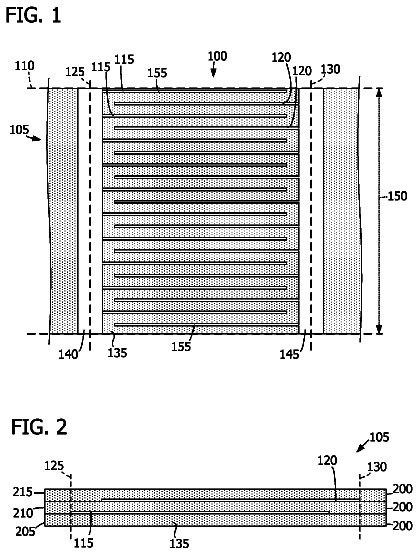
A printed wiring board (PWB) including one or more embedded capacitors.
US 8,717,804 B2 · Assignee: Kabushiki Kaisha Toshiba · Inventors: Toda; Haruki
Sheet 1 of 19 from the published document. All sheets in the USPTO PDF
A programmable resistance memory device includes a semiconductor substrate, at least one cell array, in which memory cells are arranged formed above the semiconductor substrate. Each of the memory cells has a stack structure of a programmable resistance element and an access element, the programmable resistance element storing a high resistance state or a low resistance state determined due to the polarity of voltage application in a non-volatile manner. The access element has such a resistance value in an off-state in a certain voltage range that is ten time or more as high as that in a select state. A read/write circuit is formed on a semiconductor substrate as underlying the cell array for data reading and data writing in communication with the cell array.
Recently, there have been proposed some memory devices having programmable resistance elements. One of these memory devices is known as a phase change memory which uses phase transition between an amorphous state and a crystalline state of a memory material (for example, U.S. Pat. No. 6,314,014B1). In such a phase change memory device, by controlling the current of a chalcogenide cell, reversible switching may be performed between a crystalline state (i.e. low resistance state) and an amorphous state (i.e. high resistance state). By applying a large current to a cell so as to cause the cell chalcogenide to be melted, then rapidly cooled down it, a low resistance state may be written. Annealing the chalcogenide to such a degree as to crystallize it without melting, and a high resistance state may be written. Therefore, it is possible to obtain an electrically rewritable non-volatile memor
1 of 19 drawing sheets so far from the published document, cropped to the drawing. Every sheet is in the USPTO PDF.
What the patent claimed, word for word. All of it is now free to use.
This invention relates to a programmable resistance memory device for storing a resistance state as data in a non-volatile manner, with a programmable resistance element which is switchable between a low resistance state and a high resistance state by reversing the polarity of voltage application.
Recently, there have been proposed some memory devices having programmable resistance elements. One of these memory devices is known as a phase change memory which uses phase transition between an amorphous state and a crystalline state of a memory material (for example, U.S. Pat. No. 6,314,014B1). In such a phase change memory device, by controlling the current of a chalcogenide cell, reversible switching may be performed between a crystalline state (i.e. low resistance state) and an amorphous state (i.e. high resistance state). By applying a large current to a cell so as to cause the cell chalcogenide to be melted, then rapidly cooled down it, a low resistance state may be written. Annealing the chalcogenide to such a degree as to crystallize it without melting, and a high resistance state may be written. Therefore, it is possible to obtain an electrically rewritable non-volatile memory device.
Other programmable resistance memories have been proposed as including programmable resistances switchable between a low resistance state and a high resistance state by reversing the polarity of voltage application. One of these has an ion conductor formed of a chalcogenide containing metals (for example, U.S. Pat. No. 6,418,049B1), and another one has a polymer in which conductive particles are dispersed (for example, U.S. Pat. No. 6,072,716). In these memories, dendrite growth and retraction thereof in a solid by voltage application are used. In order to write a low resistance state into a cell, a voltage is applied between the anode and cathode of a cell in such a polarity that the anode is positive. As a result, a dendrite grows from the cathode to reach the anode, whereby the cell comesto be in a low resistance state. A reverse voltage application retracts the dendrite to cause the cell to be in a high resistance state. Such a resistance change is reversible, and the low resistance state and the high resistance state may be stored in a non-volatile manner.
It has been suggested that it is possible to achieve an electrically rewritable non-volatile memory with a high density by use of such a programmable resistance. However, there has not been proposed a detailed configuration of a cell array and a read/write circuit thereof. In order to achieve a practical non-volatile memory with a high density and a high performance, how to combine the programmable resistance with what kinds of switching devices for constituting a cell array, how to construct the read/write circuit in communication with the cell array, and the like become important technical issues.
A programmable resistance memory device according to one aspect of the present invention includes:
a semiconductor substrate;
at least one cell array, in which memory cells are arranged, formed above the semiconductor substrate, each the memory cell having a stack structure of a programmable resistance element and an access element, the programmable resistance element storing a high resistance state or a low resistance state determined due to the polarity of voltage application in a non-volatile manner, the access element having such a resistance value in an off-state in a certain voltage range that is ten times or more as high as that in a select state; and
a read/write circuit formed on the semiconductor substrate as underlying the cell array for data reading and data writing in communication with the cell array.
FIG. 1 is a diagram for explaining the principle of data write for a programmable resistance memory element according to an embodiment of the present invention.
FIG. 2 shows a basic cell array and a voltage application mode thereof for a selected cell according to the embodiment.
FIG. 3 shows another voltage application mode for the selected cell in the basic cell array.
FIG. 4 shows a read/write voltage relationship for a unit cell.
FIG. 5 shows a cell characteristic for explaining a write principle.
FIG. 6 shows a cell characteristic for explaining a read principle.
FIG. 7 shows a layout of a three-dimensional cell array according to the embodiment.
FIG. 8 is a sectional diagram as taken along line I-I' of the three-dimensional cell array shown in FIG. 7.
FIG. 9 is a sectional diagram of another three-dimensional cell array.
FIG. 10 shows an equivalent circuit of the three-dimensional cell array.
FIG. 11 shows a resistance distribution of memory cells.
FIG. 12 shows a resistance distribution of the three-dimensional cell array according to the embodiment.
FIG. 13 shows a pair cell configuration method according to the embodiment.
FIG. 14 is a diagram showing operational wave forms for explanation of data read according to the embodiment.
FIG. 15 is a diagram showing operation wave forms for explanation of data write according to the embodiment.
FIG. 16 is a diagram showing operation wave forms for explanation of data write for a two pair cell in adjacent two cell arrays.
FIG. 17 shows another pair cell configuration method.
FIG. 18 is a perspective view showing a stack structure of the three-dimensional cell array and a read/write circuit thereof according to the embodiment.
FIG. 19 is a cross-sectional diagram showing the interconnection relationship between bit lines of the cell array and the read/write circuit.
FIG. 20 is a cross-sectional diagram showing the relationship between word lines and the read/write circuit.
FIG. 21 is a diagram showing a layout of the read/write circuit.
FIG. 22 is a diagram showing the word line select circuit portion of the read/write circuit.
FIG. 23 is a diagram showing the bit line select circuit portion of the read/write circuit.
FIG. 24 shows a main portion layout of the transistor circuit shown in FIGS. 22 and 23.
FIG. 25 is a perspective view of the cell array state after the bit line formation.
FIG. 26 is a perspective view of the cell array state after the memory cell formation on the bit lines.
FIG. 27 is a perspective view of the cell array state after the word line formation.
FIGS. 28A to 28C are cross-sectional views showing the word line forming process.
FIG. 1 shows a principle configuration of a programmable resistance (variable resistance) VR used in the present invention. The programmable resistance VR is formed of a resistance film 3 serving as a memory material, and cathode and anode electrodes 1 and 2 sandwiching the resistance film 3. The resistance film 3 is, for example, an ion conductor (solid electrolyte) formed of a chalcogenide containing metal ions such as silver, copperand the like. For example, Ge--S, Ge--Se and the like may be used as the chalcogenide. In the case that the resistance film 3 is formed of the above-described chalcogenide, the electrodes 1, 2 are formed containing silver.
The resistance film 3 stores, for example, a high resistance state as a data "0" and a low resistance state as a data "1". In this programmable resistance VR, by applying a positive anode-cathode voltage (V.sub.AK>0) that is over a threshold value, and a data "1" will be written. By applying a negative anode-cathode voltage (V.sub.AK<0) that is over a threshold value, and a data "0" will be written. When "1" data is written, as a result of the voltage application of V.sub.AK>0, a conductive dendrite 4 grows from the cathode electrode 1 toward the anode electrode 2 in the resistance film 3 as shown in FIG. 1. When the dendrite 4 reaches the anode electrode 2, the low resistance state (data "1") is obtained. By applying a reverse voltage, and the dendrite 4 is retracted or broken, whereby the high resistance state (data "0") is obtained. Such a low resistance state and a high resistance state may be statically held as long as a voltage is not applied over the threshold.
It should be appreciated that the resistance film 3 may be formed of a polymer in which conductive particles are dispersed (for example, carbon polymer in which carbon black particles are dispersed). In this case, a low resistance state and a high resistance state are reversibly written based on the same principle as above.
The principle of the above-described memory operation is based on a mechanism as described below. An ion conductor or a polymer is amorphous, and potential barriers are formed at random and statically therein. In addition, in the potential barrier distribution, potential valleys are formed continuously from the cathode to the anode. By dispersing some of metals in such a solid material, and it is possible to move metal ions along the potential valleys due to electric field application. When a voltage is applied in such a polarity that the anode side is positive, metal ions move toward the cathode, and metal dendrite grows from the cathode electrode. Reverse the polarity of the electric field, and the metals in the dendrite are charged and separated from the dendrite, and move toward the cathode along the potential valleys. As a result, the dendrite may be retracted.
Data read of such a programmable resistance VR may be performed by current monitoring when a voltage is applied to the programmable resistance VR at a level such that dendrite growth and retraction thereof do not occur. Alternatively, it is possible to use a large read voltage without data disturbance in a condition that it has a polarity so as to accelerate the data "0", "1" state.
FIG. 2 shows a basic cell array of a programmable resistance memory in accordance with an embodiment, with respect to a 3.times.3 cell matrix. A plurality of first wirings (hereinafter, bit lines BL) are provided in parallel, and a plurality of second wirings (hereinafter, word lines WL) are provided to cross the bit lines BL. Memory cells MC are laid out at the respective crossing points of these word lines WL and bit lines BL. The memory cell MC is a series-connection circuit of a programmable resistance VR and a Zener diode ZD. The anode of Zener diode ZD is connected to word lines WL.
In a non-select state, the bit lines BL are held at a high level voltage V.sub.H, and the word lines WL are held at a low level voltage V.sub.L. In this state, Zener diodes ZD are in a reverse-biased state and thus are in an off-state. FIG. 2 shows a case such that cell selection is performed by use of a forward-bias characteristic of the Zener diode ZD. In detail, in order to select a cell MC which is surrounded by broken lines, a selected word line WL is held at the high level voltage V.sub.H, and a selected bit line BL is held at the low level voltage V.sub.L; whereby, at the selected cell, its diode ZD becomes forward-biased to be in an on-state, and a voltage is applied to one programmable resistance VR.
FIG. 3 shows a case such that a reverse bias is applied to the programmable resistance VR in the same cell array as shown in FIG. 2. In this case, breakdown of the Zener diode ZD is used. Zener breakdown is generated by band to band tunnelling of the diode junction, and breakdown start voltage (Zener voltage) Vz may be controlled by the impurity concentration of the diode. Similarly to FIG. 2, in a non-select state, the bit lines BL are held at a high level voltage V.sub.H, and the word lines WL are held at a low level voltage V.sub.L. In order to select a cell MC which is surrounded by broken lines, a selected word line WL is held at a low level voltage V.sub.LL lower than V.sub.L, and a selected bit line BL is held at a high low level voltage V.sub.HH higher than V.sub.H (for example, V.sub.LL=V.sub.L-.DELTA., V.sub.HH=V.sub.H+.DELTA., where .DELTA. is a voltage level variation); whereby, at the selected cell, a large backward bias is applied to the diode ZD, thereby causing it breakdown. As a result, a voltage with a polarity opposite to that in FIG. 2 may be applied to one programmable resistance VR.
The above-described level relationship is an example. For example, in FIG. 2, although the non-selected bit lines and selected word line are set at the same high level voltage V.sub.H, and non-selected word lines and selected bit line are set at the same low level voltage V.sub.L, it is not necessary to use the same levels in these cases. With respect to the voltage variation .DELTA. used in the select mode in FIG. 3, it is not necessary to use the same value for the bit line and word line.
In this embodiment, the cell selection method in which the forward bias characteristic of the diode is used as shown in FIG. 2, is used for "0" data write and data read; and the cell selection method in which the backward breakdown of the diode is used as shown in FIG. 3, is used for "1" data write. Giving attention to one memory cell, read and write characteristics will be described in detail, referring to FIGS. 4 and 5.
FIG. 4 shows a relationship between a read voltage Vr, a write voltage Vw and a voltage of Zener diode ZD. Programmable resistance VR is connected with such a polarity that anode (A) thereof is connected to the bit line BL. The read voltage Vr and write voltage Vw are ones that are applied between word line WL and bit line BL.
FIG. 5 shows characteristic changes of the programmable resistance VR in accordance with write operations by use of a voltage (V)-current (I) characteristic of the diode ZD and a V-I characteristic (i.e., load line) of the programmable resistance VR. In the first quadrant, a forward-bias characteristic curve 50 of the diode ZD is shown. This is expressed as follows; I=I0{exp(qV/kT)-1}. In the third quadrant, shown are backward-bias characteristic curves 51a, 51b of the diode ZD. In the non-select state, the voltage applied to the cell is V.sub.L-V.sub.H, thus the diode ZD is held at a high-impedance off-state on the curve 51a.
In the first quadrant of FIG. 5, "0" write operation is performed as follows. Apply a write voltage Vw(0)=V.sub.H-V.sub.L in such a condition that Zener diode ZD becomes in an on-state, and the cell held in a "1" data state (i.e., low resistive state) 53 is written into a "0" data state (i.e., high resistive state) 54. In principle, it is possible to use the first quadrant characteristic for "0" writing or for "1" writing. However, since it is required to use this quadrant for cell data reading as described later, "0" write operation is performed in the first quadrant. This can be said, in other words, that the programmable resistance VR is connected with such a polarity that anode (A) thereof is connected to the bit line BL in the cell array configuration shown in FIGS. 2 to 4. Corresponding with the write voltage application, a load line 53 of "1" data state changes to a load line 54 of "0" data state, as shown by an arrow, as a result of that the dendrite of the programmable resistance is retracted, and resistance value thereof becomes high.
In order to cause the programmable resistance of "1" data to take place, it is required that a voltage higher than a certain level is applied to the programmable resistance. Such a level is shown as a "0" write threshold value VT in FIG. 5. VT is expressed in a direction with reference to Vw
as a voltage applied to the programmable resistance VR. If the cross point B1 between the forward bias characteristic curve 50 of the Zener diode ZD and the load line 53 of "1" data state of the programmable resistance is positioned between the origin and Vw(0)-VT, "0" write may be entered into the programmable resistance. As described above, by using the first quadrant for "0" write, and it becomes difficult for a write error to occur in the programmable resistance in a read mode. The reason of this will be described in detail later.
In the third quadrant, "1" write is performed. In this case, by applying a large backward bias, it may cause the Zener diode to breakdown. It allows current with an approximately constant voltage. In the drawing, "1" write operation is shown as follows; when write voltage Vw(1)=V.sub.LL-V.sub.HH is applied as being over the breakdown voltage (Zener voltage) Vz, the programmable resistance VR changes from a high resistive state 56 of "0" data to a low resistive state 55 of "1" data. Load lines 56, 55, which express "0", "1" states respectively, have inclinations in correspondence with resistance values. Therefore, these are in parallel with the load lines 53, 54 in the first quadrant, respectively. In this case, it is also required for successfully writing to the programmable resistance that a voltage higher than a threshold value VT is applied to it. This threshold value VT is expressed in a positive direction with reference to Vw(1). If the cross point B2 between the breakdown characteristic curve 51b of the Zener diode ZD and the load line 56 of "0" data state of the programmable resistance is positioned between the origin and Vw(1)+VT, "1" write may be entered into the programmable resistance. Voltages V.sub.LL, V.sub.HH and the like are selected in such a condition that sufficiently high voltage is applied to the programmable resistance.
If the resistance value of "1" data written programmable resistance is too low, a large current will flow through the Zener diode ZD, thereby causing thermal breakdown. Therefore, it is required to give attention to the current value. Corresponding to some cases, it will be necessary to include a current limiter.
If the third quadrant is used for "0" writing, there is not any danger of thermal breakdown, because the load line variation due to writing is in such a direction that the current value decreases. In this case, however, since it is required to use the first quadrant for "1" writing, the possibility of erroneous writing in a read operation is certain.
In FIG. 5, voltage variations C1 to C3, which are applied to non-selected cells during selective writing operation for the cell array shown in FIGS. 2 and 3, are shown. C1 is a voltage variation of non-selected cells along the selected bit line and selected word line during "0" data writing shown in FIG. 2; C2 is a voltage variation of non-selected cells along the selected bit line and selected word line during "1" data writing shown in FIG. 3; and C3 is a voltage variation of non-selected cells along the selected bit line and selected word line in such cases that during a "1" writing operation for a cell as shown in FIG. 3, "0" writing is performed for another cell as shown in FIG. 2. Such cases are not used in the above-described write operation. It is required that these voltage variations C1 to C3 are insufficient to break data the non-selected cells. Therefore, it is necessary for selecting the values of V.sub.H, V.sub.HH, V.sub.L and V.sub.LL in such a condition that the voltage variations do not cause the Zener diodes of the non-selected cells to be forward-biased to turn on, or do not cause those breakdown in the backward-bias direction.
FIG. 6 shows a characteristic of read operation which is performed in the first quadrant, with the "0" write characteristic (shown by broken lines). Since it is necessary to perform a read operation with a low voltage necessary for preventing the cells from erroneous write, the read operation in accordance with this embodiment is performed in the first quadrant similarly to "0" write. For example, in a read mode, the high level voltage VH is applied to a selected word line, and a low level voltage V.sub.Lr, which is higher than V.sub.L, is applied to a selected bit line. At this time, detection of a current difference or a voltage difference between crossing points S0 and S1 of the forward-biased characteristic curve 50 of the Zener diode and the load lines 58, 57 of "0", "1" data by a sense amplifier, and read data may be determined.
In the above-described read operation, it is required to prevent the cell from erroneous write due to the read voltage application. As shown in FIG. 6, as long as the voltage applied to the programmable resistance is set at lower than the threshold value VT in the "1" data read operation, no erroneous writes occur. In FIG. 6, in the "0" data read operation, a voltage slightly higher than the threshold value VT is applied to the programmable resistance. However, this becomes a "0" write mode. That is, a "0" read operation becomes a "0" rewrite operation, thereby not being an erroneous write.
As previously described, it is possible to use the first quadrant for "1" data writing in principle. However, in such the case, a "0" read operation becomes a weak "1" write mode. To avoid such the mode, it is preferable to use the first quadrant for "0" write operations.
As described above, in the read scheme of FIG. 6, as long as that the crossing point S1 for "1" data reading is in the voltage range between Vr and Vr-VT, no erroneous writes occur. In other words, it is possible to set the read voltage Vr without considering the crossing point S0 for "0" data reading. Therefore, a sense margin and a sense speed may be improved. Supposing that the third quadrant is used for data read operation, since Zener voltage Vz is approximately constant, it is difficult to obtain a sense margin necessary for preventing the erroneous write.
As above-explained, in this embodiment, a Zener diode serves as an access element for applying voltages to the programmable resistance in opposite polarities, and the forward bias characteristic and the backward bias breakdown characteristic thereof are be used. In the backward bias characteristic, there is a voltage region, in which a resistance value is regarded as being approximately infinite, under Zener voltage Vz. This is an important characteristic required for the access element of the programmable resistance. In general, it is required of the access element to have such a resistance value in an off-state in a certain voltage range that is ten times or more as high as that in a select state. In consideration of this, it should be appreciated that other access elements, for example, a PN junction diode, a Shottky diode and the like, may be used as long as that they are held in a high-resistive off-state in a certain voltage range. In addition, it should be appreciated that the programmable resistance element may be formed of not only above-described materials but also such a material which carries current in different directions corresponding to the polarity of voltage application to have different resistance values corresponding to the current directions.
So far, the configuration of the basic cell array and the principle of the data read/write operation have been explained. In this embodiment, a three-dimensional cell array structure in which a plurality of cell arrays are stacked above a semiconductor substrate is utilized. Such a three dimensional cell array will be explained below.
FIGS. 7 and 8 show a layout and a cross section along I-I' line thereof of a three-dimensional (3D) cell array including four-layer stacked cell arrays MA0 to MA3. In these figures, the same reference numerals are used as the same parts or components in the respective cell arrays, which numerals are distinguished between the cell arrays by addition of suffixes "a", "b", "c" and "d" thereto, and also distinguished between the shared portions of each two cell arrays by addition of suffixes "ab", "bc" and "cd".
A silicon substrate 10 is covered with an insulator film such as a silicon dioxide film. Above the substrate, a plurality of bit lines (BL) 12a are arranged in parallel with each other. Pillar-type memory cells MC are arranged on each bit line 12a at a certain pitch, each of which has a programmable resistance element VR and a Zener diode ZD stacked thereon. Word lines (WL) 18ab are formed to commonly connect the upper ends of the memory cells MC in a direction perpendicular to the bit lines 12a, whereby first cell array MA0 is formed.
As above-described, the programmable resistance element VR is written into a "0" state by applying a high level voltage to the word line WL and a low level voltage to the bit line BL to cause it to be forward-biased. Therefore, the programmable resistance element VR is disposed with such a polarity that cathode and anode thereof are to be connected to the word line WL and bit line BL, respectively. This is the same for every cell array stacked.
In detail, the memory cells MC are formed by patterning laminated layers having programmable resistance element layer 13a, an ohmic electrode 14a, an n.sup.+-type silicon layer 15a and a p+-type silicon layer 16a. The programmable resistance element layer 13a is, as shown in FIG. 1, formed of an ion conductor containing a specified metal or a polymer sandwiched by anode and cathode electrodes. An interlayer dielectric film 17 is buried around the memory cells MC to planarize the cell array MA0.
Second cell array MA1 is formed to share the word lines (WL0) 18ab with the first cell array MA0. In detail, pillar-type memory cells MC are arranged on each word line 18ab at a certain pitch, each of which is formed by patterning the laminated films of a p.sup.+-type silicon film 16b, an n.sup.+-type silicon film 15b, an ohmic electrode 14b and a programmable resistance element film 13b to have a stacked structure of a Zener diode ZD and a programmable resistance element VR. The cell layout is the same as that of the first cell array MA0. Bit lines (BL1) 12ab are patterned to commonly connect the programmable resistance element layers 13b arranged along a direction perpendicular to the word lines 18ab. An interlayer dielectric film 19 is buried around the memory cells MC to planarize the cell array MA1.
The stacked structure of third and fourth cell arrays MA2 and MA3 is periodically formed as similar to the first and second cell arrays MA0 and MA1. Bit lines (BL1) 12bc are shared with the second cell array MA1 and the third cell array MA2. The third cell array MA2 and the fourth cell array MA3 share the word lines (WL1) 18cd with each other. Bit lines (BL0) 12a of the lowest cell array MA0 and bit lines (BL3) 12d of the uppermost cell array MA3 are independently prepared, respectively. Although the cross section along II-II' line of FIG. 7 is not shown, the memory cells MC are disposed on the continuously formed word lines WL at the same pitch as the bit lines on this cross section.
As shown in FIG. 7, the bit lines BL and word lines WL of each cell array are formed with such a pattern that they are rotated by 90.degree. to each other, and memory cells MC are sandwiched therebetween at the respective crossing points. For example, the word lines WL and bit lines BL are formed with a line/space=1F/1F, where F is the minimum device feature size, thereby achieving the unit cell area of 4F.sup.2. In order to form such the structure, it is possible to use in the patterning process of the memory cells MC two exposures with an exposure mask used for patterning the word lines or the bit lines. In detail, in the lithography process for the laminated layers used for memory cells, exposures are performed twice with an exposure mask in such a manner that the mask is rotated by 90.degree. between the respective exposure steps. Then, the laminated layers are etched so as to retain overlap portions at the two exposure steps, and the memory cells MC are disposed at the respective crossing portions of the bit lines BL and the word lines WL.
In FIG. 8, the programmable resistance element layers 13 are disposed only at the cross portions of the bit lines BL and the word lines WL. In contrast to this, in such a case that the leak current of the programmable resistance element layer 13 is negligibly small, the programmable resistance element layer 13 may be retained without patterning, as shown in FIG. 9. In this case, the sandwiched portions between the diode ZD and the bit lines or the word lines within the programmable resistance element layer 13 materially function as the programmable resistance elements VR.
FIG. 10 shows a three-dimensional equivalent circuit of the 3D cell array formed as above-described. In order to prevent the bit lines from mutual interference, each two bit lines constitute a pair, and another bit line is disposed between the pair of bit lines. BL00, /BL00, BL01, /BL01, . . . are bit line pairs of the first cell array MA0; BL10, /BL10, BL11, /BL11, . . . are shared bit line pairs between the second and third cell array MA1 and MA2; and BL20, /BL20, BL21, /BL21, . . . are bit line pairs of the fourth cell array MA3. Further, WL0 (WL00, WL01, . . . ) are shared word lines between the first and second cell arrays MA0 and MA1; and WL1 (WL10, WL11, . . . ) are shared word lines between the third and fourth cell arrays MA2 and MA3.
In the above-described 3D cell array in which many memory cells are integrated, variation of cell characteristics causes trouble. In detail, since the resistance value of the programmable resistance element VR is determined by dendrite growth and retraction thereof, variation occurs due to a history thereof, environment and the like. FIG. 11 schematically shows a distribution of the resistance values of data "0", "1". If there is no overlap region, as shown in FIG. 11, between the resistance values of "0" and "1", it is possible to distinguish between "0" and "1" by use of a reference resistance Rref. However, in the 3D cell array that has numerous cells, it becomes difficult to set such a reference resistance Rref. FIG. 12 schematically shows such a situation as above-described. Groups A, B, C and D include nearly disposed plural cells, respectively. By giving attention to each the group, and it is possible to set a reference resistance Rref. However, with respect to the entire cell array, it becomes difficult or impossible.
In consideration of the above-described view points, in this embodiment, two nearby cells constitute a cell pair for storing complementary data therein in such a manner that data "0" is stored in one cell and data "1" is stored in the other cell. Read operation is done by detecting the difference between cell currents of the two cells constituting the pair. By use of this scheme, even if there is a partial overlap between the high resistive state distribution and the low resistive distribution in the entire 3D cell array, it is possible to precisely read/write the cell data.
In FIG. 10, two cell pairs are typically shown as follows: two cells connected to a pair of bit lines BL00 and BL00, respectively, with sharing a word line WL00 in the cell array MA0, being constitute one cell pair, one of which is a true cell, T-cell0, and the other is a complementary cell, C-cell0; and two cells connected to a pair of bit lines BL10 and /BL10, respectively, sharing a word line WL10 in the cell array MA1, being constituted to another pair cell, one of which is a true cell, T-cell1, and the other is a complementary cell, C-cell1. In every pair of cells, a positive logic value of a binary data is stored in the true cell, and a negative logic value is stored in the complementary cell. Similar cell pairs are selected in the cell arrays MA2 and MA3. In FIG. 10, cell currents at the respective read selection times are shown by arrows.
Data read/write methods in such the case that two memory cells constitute a cell pair will be described in detail below. FIG. 13 shows two cell pairs in two cell arrays disposed adjacent up and down to have a shared word line WL. Data read operations for these two cell pairs may be simultaneously performed by use of operation waveforms as shown in FIG. 14. In a non-select mode, V.sub.H-V.sub.L between the bit lines and the word lines is a hold voltage which holds the memory cells in such a non-select state that diodes thereof are backward-biased to be in a high resistive off-state.
In a read selection mode as shown in FIG. 14, a high level voltage VH is applied to the word line WL which is held at a low level voltage V.sub.L at a non-select time. At the same time, a low level voltage V.sub.Lr (>V.sub.L) is applied to the bit lines BL0, /BL0, BL1 and /BL1 which are held at high level voltage V.sub.H at the non-select time. In other words, between the selected word line WL and the selected bit line pairs BL0, /BL0 and BL1, /BL1, a read voltage Vr=V.sub.H-V.sub.Lr is applied to forward-bias the selected cells. As a result, cell currents flow in the respective cells as above-explained with FIG. 6. Detection of the cell current differences between the pair of bit lines BL0, /BL0, and between the pair of bit lines BL1, /BL1 is by sense amps, and cell data of the respective cell pairs may be determined. Since each cell pair is constituted by two neighbouring cells to store complementary data, it is possible to precisely sense the cell data.
Next, data write operations into cell pairs will be described. Although a pair of cells store a data "0" in one cell and a data "1" in the other cell, "0" and "1" write voltages applied between the word line and the bit line have to be opposite each other as above-described. This means that it is impossible to simultaneously write data into the true cell, T-cell, and the complementary cell, C-cell, which share a word line. Therefore, it is required to perform data write operations for a cell pair twice.
FIG. 15 shows waveforms of "0" data writing (i.e., T-cell="0", C-cell="1") and "1" data writing (i.e., T-cell="1", C-cell="0") into a cell pair. In order to write "0" data, with respect to the bit lines which are held at the high level voltage V.sub.H in the non-select mode, a low level pulse voltage V.sub.L is applied to one bit line pair, BL0 (or BL1), and a high level pulse voltage V.sub.HH higher than V.sub.H is applied to the other, /BL0 (or /BL1). A high level voltage V.sub.H is applied to the word line WL in the former half T1 of the above-described bit line selection period, and a low level voltage V.sub.LL lower than V.sub.L is applied to the same in the latter half T2.
As a result, in the former half T1, "0" write voltage, Vw(0)=V.sub.H-V.sub.L, is applied to one cell, T-cell, of the pair cell to forward-bias the diode thereof due to the high level voltage V.sub.H of the word line WL and the low level voltage V.sub.L of the bit line BL0 (or BL1), whereby the T-cell is written into a "0" data state. At this time, since the voltage applied to the other cell, C-cell, is V.sub.H-V.sub.HH, the diode of C-cell is held at an off-state. Therefore, no error data are written into the C-cell. In the latter half T2, "1" write voltage, Vw(1)=V.sub.LL-V.sub.HH, is applied to the other cell, C-cell, of the pair cell to cause the diode thereof to breakdown due to the low level voltage V.sub.LL of the word line WL and the high level voltage V.sub.HH of the bit line /BL0 (or /BL1), whereby the C-cell is written into a "1" data state. At this time, the voltage applied to the cell T-cell, in which a data has been written, is V.sub.LL-V.sub.L. Since the diode of the T-cell is held at an off-state in this condition, no error data are written into the T-cell.
In order to write "1" data, one of the bit line pair, BL0 (or BL1), is boosted to the higher level voltage V.sub.HH from the high level voltage V.sub.H, and the other, /BL0 (or /BL1), is pulled down to the low level voltage V.sub.L from the high level voltage V.sub.H. And, similarly to the "0" write mode, the high level voltage V.sub.H is applied to the word line WL in the former half T1 of the above-described bit line selection period, and then the low level voltage V.sub.LL is applied to the same in the latter half T2.
As a result, in the former half T1, one of the cell pair, C-cell, is written into a "0" data state because the cell diode is forward-biased due to the high level voltage V.sub.H of the word line WL and the low level voltage V.sub.L of the bit line /BL0 (or /BL1). In the latter half T2, the other cell, T-cell, is written into a "1" data state because the low level voltage V.sub.LL of the word line WL and the high level voltage V.sub.HH of the bit line BL0 (or BL1) cause the cell diode to breakdown. No erroneous writes occur in both the former half for "0" writing and the latter half for "1" writing, similarly to the above-described "0" writing mode.
As apparent from FIG. 15, "0", "1" writing into a cell pair may be selected by reversing the voltages applied to the bit line pair, while the same voltage is applied to the word line. Therefore, it is possible to perform simultaneous data writing into two pairs of cells with a shared word line.
FIG. 16 shows in detail waveforms of simultaneous data writing into two cell pairs, (T-cell 0, C-cell 0) and (T-cell1, C-cell1), which are adjacent up and down with a shared word line WL00. The data combinations of the two pair cells are expresses as four values "00", "01", "10" and "11". Corresponding to the four values data, in FIG. 16, bit data of T-cell1, C-cell1, T-cell0 and C-cell0 are shown at upsides of the respective waveforms. To the respective bit line pairs, (BL00, BL00), (BL10, /BL10), the high level voltage V.sub.HH and the low level voltage V.sub.L are applied in correspondence with to-be-written data. The voltages applied to the word line WL00 are changed all the same for the four data such that the high level voltage V.sub.H and the low level voltage V.sub.L are applied in the former half and the latter half respectively in the bit line selection period, similarly to that in FIG. 15. By use of such waveforms, two cell pairs may be simultaneously written.
As is apparent from the above-described write operations, it should be appreciated that it is possible to simultaneously access the respective plural cell pairs within the first and second cell arrays MA0 and MA1 with shared word lines. Similarly, it is possible to simultaneously access the respective plural cell pairs within the third and fourth cell arrays MA2 and MA3 with shared word lines. In contrast to this, note that it is not possible to simultaneously access the second and third cell arrays MA1 and MA2 with shared bit lines.
Up to this point, it has been explained that such a cell pair configuration laterally neighbouring two memory cells constitute a cell pair in each cell array layer in the three-dimensional cell array. However, the cell pair configuration method is not so limited. As shown in FIG. 17, it is possible to select a vertically neighbouring pair of memory cells MC with a shared word line WL so as to constitute a cell pair (i.e., a true cell, T-cell, and a complementary cell, C-cell). In this case, the bit lines BL0, BL1 which belong to different cell arrays become a pair of bit lines to be connected to the pair cell.
FIG. 18 is a schematic perspective view showing a stacking state of cell blocks 100 and a read/write circuit 200 and interconnection relationships therebetween. Each cell block 100 corresponds to the above-described 3D cell array with four layers. A 3D cell array is, when necessary, divided into a plurality of cell blocks 100 with a predetermined capacity. In FIG. 18, two cell blocks 100 are arranged in a direction along the bit lines.
As shown in FIG. 18, the read/write circuit 200, which is used for data reading and writing in communication with the cell block 100, underlies the cell block 100. The read/write circuit 200 is formed such that the main portion thereof is disposed within a rectangular cell layout region 210 defined on the substrate 10, above which the cell block 100 is stacked. The cell layout region 210 is defined by two boundaries A1 and A2 in the direction of the bit lines, and by two boundaries B1 and B2 in the direction of the word lines.
The description continues in the full USPTO document.
About 6,879 words. The USPTO PDF has it with every drawing.
Fees are due 3.5, 7.5 and 11.5 years after grant. This patent expired on May 6, 2026, so the fee marked "not paid" was the one that went unpaid.
Programmable resistance memory device
Filed Mar 2003 · published Nov 2006Three-dimensional programmable resistance memory device with a read/write circuit stacked under a memory cell array
Filed Mar 2003 · granted Oct 2009THREE DIMENSIONAL PROGRAMMABLE RESISTANCE MEMORY DEVICE WITH A READ/WRITE CIRCUIT STACKED UNDER A MEMORY CELL ARRAY
Filed Sep 2009 · published Jul 2010Three dimensional programmable resistance memory device with a read/write circuit stacked under a memory cell array
Filed Sep 2009 · granted Nov 2010THREE DIMENSIONAL PROGRAMMABLE RESISTANCE MEMORY DEVICE WITH A READ/WRITE CIRCUIT STACKED UNDER A MEMORY CELL ARRAY
Filed Oct 2010 · published Jan 2011Three-dimensional programmable resistance memory device with a read/write circuit stacked under a memory cell array
Filed Oct 2010 · granted Jan 2012THREE DIMENSIONAL PROGRAMMABLE RESISTANCE MEMORY DEVICE WITH A READ/WRITE CIRCUIT STACKED UNDER A MEMORY CELL ARRAY
Filed Dec 2011 · published Apr 2012Three dimensional programmable resistance memory device with a read/write circuit stacked under a memory cell array
Filed Dec 2011 · granted May 2014Earlier publications, parents and continuations. None of them can still be enforced, or this patent would not be listed.
Prior art cited by the examiner or applicant. Useful when you check your own idea for novelty.
Everything on this page comes from the documents linked above.