Background of the invention
1. Field of the invention
The present invention relates to a technique capable of easily eliminating or reducing uneven density.
2. Description of the related art
An image forming section of a conventional image processing apparatus includes a plurality of modules, such as a photosensitive drum, a charging device, an exposure device, a developing device, and a transfer device. In the above-described image forming section, the charging device uniformly charges the photosensitive drum while the photosensitive drum is rotating.
Next, the exposure device selectively exposes a charged photosensitive drum surface to form an electrostatic latent image on the photosensitive drum. Then, the developing device develops the electrostatic latent image formed on the photosensitive drum into a visible toner image. The transfer device transfers the obtained toner image onto a recording material.
In the above-described image forming section, uneven density (banding) may appear periodically on the photosensitive drum in a rotational direction thereof, more specifically, in a sub scanning direction. Many of the above-described modules include rotational members, such as drums, rollers, sleeves, and screws, which rotate continuously during their operations.
In general, a motor serving as a rotational power source of each module has an error in its rotational behavior. The rotational speed of each motor is variable depending on the rotational angle of a motor shaft. Therefore, for example, the rotational speed of the photosensitive drum varies periodically in accordance with the rotation of a driving motor.
According to the periodic variation in the rotational speed of the photosensitive drum, the quantity of exposure per unit area changes periodically and periodic uneven density appears on an output image. Further, the accuracy of a gear that transmits motor driving power to a rotary member becomes a cause of the uneven density.
Further, if a rotational shaft of a rotary member has a certain amount of eccentricity, for example, when the photosensitive drum has a certain amount of eccentricity, the distance between the photosensitive drum and the developing device changes periodically. Therefore, a significant amount of periodic uneven density appears due to a change in developing efficiency corresponding to the distance.
Further, the AC voltage applied to the charging and developing devices becomes a cause that may induce the periodic uneven density because the developing amount changes similarly. As described above, a general image forming section includes various modules that may induce the periodic uneven density.
Further, in a case where a device includes a plurality of modules each having a unique periodicity, a significant amount of interference may occur between two or more different frequencies and a composite periodic uneven density may appear.
To solve the above-described problem, as discussed in Japanese Patent Application Laid-Open No. 10-20579, there is a conventional technique capable of adjusting a turn-on period of an exposure device to correct the density based on a generated density variation detected by a density detection device.
Further, the image forming section can include a scanner capable of reading a final image (i.e., a test image) to detect a density distribution. The detected density distribution can be used to correct the periodic uneven density.
For example, as discussed in Japanese Patent Application Laid-Open No. 11-112810, a scanner performs a scanning operation to read a test image and detect density data in a main or sub scanning direction. Then, pixel data correction is performed using correction data generated based on the detected density data. According to any one of the above-described conventional techniques, the periodic uneven density can be reduced by performing correction having inverse characteristics in such a way as to cancel or reduce the generated density characteristics.
According to the technique discussed in Japanese Patent Application Laid-Open No. 10-20579, it is required to measure all information about periodicity, waveform, phase, and amplitude and determine correction parameters. Therefore, it is required to detect the density of an image at intervals sufficiently smaller than the periodicity of the image forming section.
Therefore, the density detection device is required to have highly accurate resolution and response. Further, to equalize the phases of a plurality of periodicities generated by respective modules, it is required to adjust the design features (e.g., an outer diameter of each module) to be the same or in an integer multiple relationship. Thus, the degrees of freedom in the design stage are reduced.
Further, according to the technique discussed in Japanese Patent Application Laid-Open No. 11-112810, it is similarly required to measure information about all of periodicity, waveform, phase, and amplitude and determine correction parameter. Thus, a large-scale device, such as the above-described scanner, is required.
Further, it is required to perform correction at intervals equivalent to an image formed on a transfer member or a paper. Therefore, the rotational periodicity of each module is required to be an integer fraction of the image. If the rotational periodicity of a module is not an integer fraction of the image, the phase of the module causes a stepwise deviation in each output. Therefore, a correction amount calculated based on an output of the scanner cannot be effectively used in the correction.
Further, each of the above-described techniques requires a memory that stores measurement data and a synchronization system that synchronizes measurement timing with correction timing. Accordingly, an apparatus having a large-scale configuration is required and it is difficult to realize a low-cost apparatus.
Summary of the invention
The present invention is directed to an image processing apparatus that can easily eliminate or reduce uneven density having periodicity unique to each module.
According to an aspect of the present invention, an image processing apparatus includes a pattern generation unit configured to cause an image forming section to generate a plurality of image patterns that have periodicity unique to the image forming section and are different from each other, a selection unit configured to select one test pattern from the generated plurality of image patterns, and an image correction unit configured to correct an image based on the test pattern selected by the selection unit.
According to an exemplary embodiment of the present invention, the uneven density having the periodicity unique to each module can be eliminated or reduced with a simple configuration.
Further features and aspects of the present invention will become apparent from the following detailed description of exemplary embodiments with reference to the attached drawings.
Brief description of the drawings
The accompanying drawings, which are incorporated in and constitute a part of the specification, illustrate exemplary embodiments, features, and aspects of the invention and, together with the description, serve to explain the principles of the invention.
FIG. 1 schematically illustrates an example configuration of an image forming section according to a first exemplary embodiment of the present invention.
FIGS. 2A to 2C schematically illustrate an example configuration of an exposure unit according to the first exemplary embodiment of the present invention.
FIG. 3 is a flowchart illustrating light quantity correction data setting processing that can be performed by a density correction unit according to the first exemplary embodiment of the present invention.
FIGS. 4A to 4C illustrate examples of output test patterns.
FIG. 5 is a flowchart illustrating light quantity correction processing that can be performed by the density correction unit according to the first exemplary embodiment of the present invention.
FIG. 6 illustrates an example of a test pattern according to a second exemplary embodiment of the present invention.
FIG. 7 is a flowchart according to a third exemplary embodiment of the present invention.
FIGS. 8A and 8B illustrate example screens of a user interface according to the third exemplary embodiment of the present invention.
FIGS. 9A and 9B are flowcharts according to a fourth exemplary embodiment of the present invention.
Description of the embodiments
Various exemplary embodiments, features, and aspects of the invention will be described in detail below with reference to the drawings.
An image forming section of an image processing apparatus generates uneven density whose variation periodicity is dependent on the periodicity of a rotational member or the AC voltage. In many cases, the variation periodicity of the uneven density can be known beforehand in the design stage of the image forming section.
Further, the waveform that indicates a variation of the density during one period has a shape substantially determined according to each module (i.e., each cause) and has a higher reproducibility. It is, therefore, feasible to prepare the waveform beforehand.
Further, in many cases, a sine wave can be used to approximate the variation periodicity occurring in an actual image forming section. Further, in a case where a waveform representing the uneven density is different from a waveform representing the correction, for example, if the uneven density occurring in a triangular waveform is corrected with a sine wave having the opposite phase, the uneven density can be reduced significantly although a higher harmonics wave may appear.
Further, the phase and the amplitude are examples of features required in correction of the uneven density. Regarding the amplitude, if a generated error is in a range from 0 to 2 times the actual amplitude, the uneven density is not so worsened compared to the non-corrected one. Therefore, an excessive accuracy is not required with respect to the amplitude.
On the other hand, regarding the phase, there is a problem arising when waves are simply added. If an applied correction has inverse characteristics in a state where a deviation amount is equal to or greater than 1/6 of the variation periodicity, the uneven density is worsened compared to the non-corrected one. Therefore, in an actual correction, it is important to determine an effective acquisition procedure for the phase and the amplitude of the uneven density.
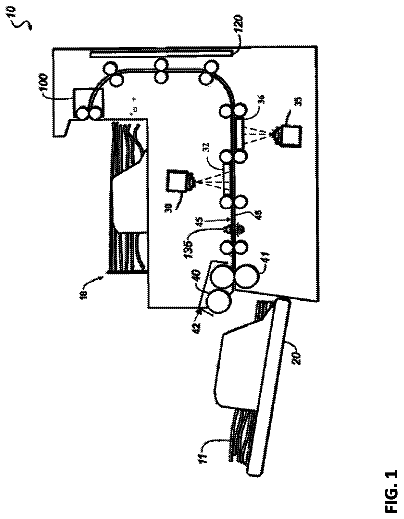
FIG. 1 schematically illustrates an example configuration of an image forming section according to a first exemplary embodiment of the present invention. The image forming section according to the present exemplary embodiment includes a plurality of (for example, "four" according to the example illustrated in FIG. 1) image forming units 10 (more specifically, 10Y, 10M, 10C, and 10K). Each image forming unit 10 can form a toner image of a predetermined color according to an electro-photographic image forming method.
Further, the image forming section includes an intermediate transfer belt 20 (an endless belt) on which toner images of different colors are successively transferred (primarily transferred) from respective image forming units 10 (10Y, 10M, 10C, and 10K). Further, the image forming section includes a secondary transfer device 30 that can collectively transfer (secondarily transfer) the toner images from the intermediate transfer belt 20 to paper P. Further, the image forming section includes a fixing device 50 that can fix the secondarily transferred toner image on the paper P.
Respective image forming units 10 (10Y, 10M, 10C, and 10K) are similar to each other in configuration, except for the color of a toner to be used. Hence, as a representative example, only the yellow image forming unit 10Y is described below in detail. The yellow image forming unit 10Y includes a photosensitive layer (not illustrated) and a photosensitive drum 11 that can rotate in a direction indicated by an arrow A.
Devices sequentially disposed around the photosensitive drum 11 are a charging device 12, an exposure unit 13, a developing device 14, a primary transfer device 15, and a cleaner 16. The charging device 12 can charge the photosensitive drum 11 to have a predetermined electric potential.
The exposure unit 13 can form an electrostatic latent image on the photosensitive drum 11 with a laser beam, in a state where the photosensitive drum 11 is charged by the charging device 12 to have a predetermined negative electric potential. The developing device 14, accommodating a corresponding color (i.e., yellow) toner, can develop an electrostatic latent image on the photosensitive drum 11 with the yellow toner.
The primary transfer device 15 can primarily transfer a toner image formed on the photosensitive drum 11 onto the intermediate transfer belt 20. The cleaner 16 can remove the residue (toner etc.) remaining on the photosensitive drum 11 after the toner image has been primarily transferred to the intermediate transfer belt 20.
The intermediate transfer belt 20 is stretched around a plurality of (for example, "six" in the present exemplary embodiment) support rollers. The intermediate transfer belt 20 can move along a circulating path defined by the plurality of support rollers. A driving roller 21 (one of the plurality of support rollers) can rotate around its rotational axis to drive the intermediate transfer belt 20 stretched around an outer cylindrical surface thereof.
The intermediate transfer belt 20 is tightened by a plurality of driven rollers 22, 23, and 26, which are freely rotatable while the intermediate transfer belt 20 is driven by the driving roller 21. A correction roller 24 is tiltable and supported at one end thereof in the axial direction. The correction roller 24 is functionally operable as a steering roller that can prevent a skew motion of the intermediate transfer belt 20, which may deviate in a direction substantially perpendicular to the conveying direction of the intermediate transfer belt 20.
A backup roller 25, around which the intermediate transfer belt 20 is stretched, is functionally operable as a constituent member of the secondary transfer device 30. A belt cleaner 27 is disposed at a position closely opposed to the driving roller 21 via the intermediate transfer belt 20. The belt cleaner 27 can remove the residue (toner etc.) remaining on the intermediate transfer belt 20 after the toner images are secondarily transferred onto the paper P.
The secondary transfer device 30 includes a secondary transfer roller 31 that can be pressed against an image carrying surface of the intermediate transfer belt 20. The secondary transfer roller 31 is opposed to the backup roller 25, which is disposed on a reverse surface side of the intermediate transfer belt 20 and serves as a counter electrode of the secondary transfer roller 31.
A power supply roller 32, which is brought into contact with the backup roller 25, can apply a secondary transfer bias whose polarity is similar to the toner charging polarity. The secondary transfer roller 31 is grounded.
A paper conveyance system includes a paper tray 40, a pair of conveyance rollers 41, a pair of registration rollers 42, an endless conveyance belt 43, and a pair of discharge rollers 44. The paper conveyance system feeds the uppermost paper P to the conveyance rollers 41 from the paper tray 40 and temporarily stops the paper P at a position corresponding to the registration rollers 42. Subsequently, the paper conveyance system sends the paper P to a secondary transfer position of the secondary transfer device 30 at predetermined timing.
Further, the paper conveyance system conveys the paper P on which toner images are secondarily transferred to the fixing device 50 via the conveyance belt 43. Then, the discharge rollers 44 discharge the paper P from the fixing device 50 to the outside of the image forming section.
Next, example image forming processing that can be performed by the image forming section is described below. If a start switch (not illustrated) is operated, the image forming section starts predetermined image forming processing. More specifically, in a case where the image forming section is a digital color copying machine, the image forming section causes a color image reading device to read a document placed on a document positioning plate (not illustrated). Then, the image forming section acquires a reading signal from the color image reading device.
Next, the image forming section causes a processing circuit to convert the obtained reading signal into a digital image signal and temporarily stores the digital image signal in a memory. Then, the image forming section performs toner image formation of respective colors based on the digital image signals of four colors, cyan (C), magenta (M), yellow (Y), and black (K), stored in the memory.
More specifically, the image forming section drives each image forming unit 10 (more specifically, 10Y, 10M, 10C, and 10K) according to the obtained digital image signal of a corresponding color.
Next, in each image forming unit 10, the exposure unit 13 irradiates the photosensitive drum 11 uniformly charged by the charging device 12 with a laser beam according to a corresponding digital image signal, to form an electrostatic latent image. Then, the developing device 14 develops the electrostatic latent image formed on the photosensitive drum 11 to form a toner image of the corresponding color. In a case where the image forming section is a printer, the image forming section performs toner image formation of each color based on a digital image signal input from an external device, such as a personal computer.
Subsequently, the primary transfer device 15 primarily transfers the toner image formed on the photosensitive drum 11 to a confronting surface of the intermediate transfer belt 20 at a primary transfer position where the photosensitive drum 11 is brought into the intermediate transfer belt 20. After the above-described primary transfer of the toner image to the intermediate transfer belt 20, the toner remaining on the photosensitive drum 11 is cleaned by the cleaner 16.
Respective toner images having been primarily transferred on the intermediate transfer belt 20, as described above, are mutually overlapped on the intermediate transfer belt 20. Then, the overlapped toner images are conveyed to the secondary transfer position in accordance with a rotational movement of the intermediate transfer belt 20. On the other hand, the paper P is conveyed to the secondary transfer position at predetermined timing. The secondary transfer roller 31 nips the paper P in a state where the behind side of the paper P is supported by the backup roller 25.
Then, under a transfer field formed between the secondary transfer roller 31 and the backup roller 25, the toner image carried on the intermediate transfer belt 20 is secondarily transferred onto the paper P at the secondary transfer position. The conveyance belt 43 conveys the paper P carrying the transferred toner image to the fixing device 50. The fixing device 50 applies heat and pressure to the paper P to fix the toner image formed thereon. Subsequently, the paper P is output to an externally provided discharge tray (not illustrated). After the above-described secondary transfer operation, the toner remaining on the intermediate transfer belt 20 is cleaned by the belt cleaner 27.
FIG. 2A illustrates an example configuration of the exposure unit 13, which is functionally operable as a unit capable of changing image forming conditions. The exposure unit 13 performs a scanning operation to expose the photosensitive drum 11 (i.e., a photosensitive member) in the following manner.
The exposure unit 13 includes a light source 101, a collimator lens 102, a cylinder lens 103, and a rotary polygonal mirror 104. The light source 101 can include a semiconductor laser. For example, the rotary polygonal mirror 104 has a hexagonal columnar body. The exposure unit 13 further includes an f.theta. lens (beam-condensing lens) 105, a folding mirror 106, a reflection mirror 107, and a Start Of Scan (SOS) sensor 108.
In the exposure unit 13, the light source 101 emits a divergent laser beam L. The collimator lens 102 converts the laser beam L into a parallel beam. The cylinder lens 103, having a refractive power only in the sub scanning direction, focuses the laser beam L, as a line image extending in the main scanning direction, in the vicinity of a deflecting reflection surface 104a of the polygonal mirror 104.
Then, the laser beam L is reflected by the deflecting reflection surface 104a of the polygonal mirror 104 while the polygonal mirror 104 is rotating around its rotational axis at a predetermined higher speed. Thus, the scanning operation is performed at a constant angular speed in the counterclockwise (i.e., in a direction indicated by an arrow C).
After the laser beam L has passed through the f.theta. lens 105, the folding mirror 106 changes the direction of the laser beam L toward the surface of the photosensitive drum 11 in such a way as to perform a scanning operation to expose the surface of the photosensitive drum 11 in a direction indicated by an arrow D.
In the present exemplary embodiment, the f.theta. lens 105 has the capability of realizing an equi-speed scanning of a light spot of the laser beam L. Further, the cylinder lens 103 can focus the above-described line image in the vicinity of the deflecting reflection surface 104a of the polygonal mirror 104. The f.theta. lens 105 focuses the light spot of the laser beam L on the surface of the photosensitive drum 11, in the sub scanning direction, with respect to the deflecting reflection surface 104a (an object point). Accordingly, the above-described scanning optical system has the capability of correcting the plane tilt of the deflecting reflection surface 104a.
Further, the laser beam L reaches the SOS sensor 108 via the reflection mirror 107 prior to the scanning operation to expose the surface of the photosensitive drum 11. More specifically, the SOS sensor 108 receives the initial laser beam L of each scanning line every time the surface of the photosensitive drum 11 is scanned with the laser beam L. Then, the SOS sensor 108 detects irradiation timing of each scanning line on the surface of the photosensitive drum 11 and generates an SOS signal indicating irradiation start timing.
The light source 101 is connected to a laser driver 109 that outputs a laser activation signal at predetermined timing based on image data to be written, which is output from an image signal generation unit (IPS) 60. The laser driver 109 performs ON/OFF control for the semiconductor laser of the light source 101 based on the image data to be written, which can be supplied from the IPS 60. Thus, the light source 101 can emit the laser beam L whose intensity corresponds to the image data to be written.
Further, the laser driver 109 is connected to an engine controller 80. The engine controller 80 includes a driving signal generation unit A 802A and a driving signal generation unit B 802B. The laser driver 109 receives a driving signal supplied from the driving signal generation unit A 802A. Further, the laser driver 109 sets the start timing to output the laser activation signal to be supplied to the semiconductor laser of the light source 101 based on the received driving signal.
Further, the laser driver 109 is connected to the SOS sensor 108 to receive the SOS signal generated by the SOS sensor 108. Then, the laser driver 109 sets the start timing to output the laser activation signal to the semiconductor laser of the light source 101 based on the SOS signal from the SOS sensor 108.
In the present exemplary embodiment, the laser driver 109 controls the semiconductor laser of the light source 101 based on the driving signal generated by the engine controller 80 as well as the SOS signal from the SOS sensor 108. The driving signal and the SOS signal are differently used in the control.
The driving signal generated by the engine controller 80 is a vertical synchronizing signal, which can be used to synchronize an operation of a module represented by the photosensitive drum 11. The SOS signal from the SOS sensor 108 is a horizontal synchronizing signal, which can be used to control the position of an image in the main scanning direction of the laser.
Further, the laser driver 109 receives a density variation signal from the density correction unit 70. The density correction unit 70 generates a signal representing a density variation in the sub scanning direction, which may be caused by rotational members of respective units, such as the photosensitive drum 11 and a developing roller equipped in the developing device 14 (see FIG. 1), and outputs the generated density variation signal to the laser driver 109.
The laser driver 109 adjusts the light quantity of the laser beam L to be emit from the semiconductor laser of the light source 101 based on the density variation signal supplied from the density correction unit 70. The light quantity adjustment of the laser beam L is performed not before the SOS signal is detected and not after the scanning operation actually starts to expose the surface of the photosensitive drum 11.
The density correction unit 70 is connected to the engine controller 80 to receive a module activation signal from the driving signal generation unit B 802B of the engine controller 80. The density correction unit 70 calculates a density variation amount based on the received module activation signal.
Hereinafter, an example adjustment of the quantity of light emitted from the laser beam L is described below. In general, the quantity of light to be used in the exposure processing is maintained at a constant power level. To this end, for example, a calibration is performed to equalize the maximum density of the image forming section with a target value.
To simplify the description, if the light quantity of the image forming section is proportional to the density, it is feasible to eliminate or reduce the uneven density by controlling the light quantity using a coefficient having inverse characteristics.
More specifically, it is now presumed that the target density is 1.0 and the density is variable in a range from 0.9 to 1.1. In this case, if the light quantity is 1.0 when the density is 1.0, the uneven density can be eliminated or reduced by setting the light quantity to have a value in a range from 1/0.9 to 1/1.1, which is equivalent to a reciprocal of the density variation.
As described above, in the present exemplary embodiment, the exposure unit 13 is controlled based on the density variation signal having been set by the density correction unit 70 in such a way as to eliminate or reduce the uneven density periodically occurring in the sub scanning direction.
Next, density variation data setting processing (i.e., light quantity correction data setting processing) that can be performed by the density correction unit 70 is described below in more detail with reference to a flowchart illustrated in FIG. 3. Further, an example configuration of the density correction unit 70 is described below with reference to FIG. 2B.
As illustrated in FIG. 2B, the density correction unit 70 includes a correction parameter storage unit 71, a pattern generation unit 72, a pattern selection unit 73, and an uneven density prediction unit 74. The density correction unit 70 executes the above-described light quantity correction data setting processing at arbitrary timing, for example, immediately after a power source of the image forming section is turned on or when a long time has elapsed.
The correction parameter storage unit 71 stores various parameters, such as color Cl, periodicity P, waveform f, amplitude A, initial phase .alpha., and driving signal count Cn, which are the causes that may induce periodicity unique to the image forming section (device unique periodicity), more specifically, periodic uneven density, for each module.
FIG. 2C illustrates a table that stores example values of respective parameters (i.e., color Cl, periodicity P, waveform f, amplitude A, initial phase .alpha., and driving signal count Cn) that may induce the uneven density, which are calculated beforehand and stored in association with each module name. In FIG. 2C, the color Cl is a factor unique to each module.
For example, each image forming unit 10 can independently perform an image forming operation for a designated one of respective colors C, M, Y, and K. Thus, a module included in the image forming unit 10K causes uneven density appearing on an image of K color. Further, the intermediate transfer belt 20 is commonly used for all colors C, M, Y, and K.
The periodicity P of each module represents the uneven density periodically appearing on a paper output from the image forming section. The periodicity P of each module can be easily calculated based on the rotational speed of the module (i.e., the number of revolutions per unit time) and the driving speed of the photosensitive drum or the intermediate transfer belt (i.e., the moving distance per unit time).
Regarding the waveform f, an appropriate pattern can be stored by acquiring a density pattern beforehand. Further, to acquire appropriate values in the subsequent processing, predetermined initial values are set for the amplitude A, the initial phase .alpha., and the driving signal count Cn of each module (e.g., amplitude A=0.1, initial phase .alpha.=0 radian, and count Cn=0).
In the present exemplary embodiment, a driving gear (not illustrated) of the photosensitive drum 11K and a driving motor of the intermediate transfer belt 20 are two representative modules that may induce the uneven density. The driving gear of the photosensitive drum 11K has a periodicity P of 2.5 mm. The driving motor of the intermediate transfer belt 20 has a periodicity P of 32.0 mm. In respective modules, the waveform f is a sine wave.
First, in step S301, the pattern generation unit 72 selects one of the modules stored in the correction parameter storage unit 71. When there is a plurality of modules, the pattern generation unit 72 selects an arbitrary module. If sequential processing is performed in steps S301 to S308, then in step S309, the density correction unit 70 determines whether the sequential processing of steps S301 to S308 has been completed for all modules.
If it is determined that the processing is not completed for all modules (NO in step S309), the density correction unit 70 repeats similar processing for each of the remaining modules. In the present exemplary embodiment, the pattern generation unit 72 selects the driving gear of the photosensitive drum 11K (i.e., the first module in the table illustrated in FIG. 2C). Then, the processing proceeds to the next step.
In step S302, the pattern generation unit 72 reads the parameters (i.e., color Cl, periodicity P, and waveform f) of the module selected in step S301 from the correction parameter storage unit 71.
Next, in step S303, the pattern generation unit 72 generates a plurality of test patterns having correction effects differentiated in initial phase .alpha. with respect to respective parameters (i.e., color Cl, periodicity P, and waveform f) of the module read in step S302.
Hereinafter, a relationship between periodicity/phase of the module and the driving signal count is described below. If a module is a cause that may induce any unevenness in density, an image includes a corresponding uneven density that appears periodically according to the periodicity of the module. In general, the driving signal of a module indicates a period of time during which the module is driven (=rotated). Therefore, the pattern generation unit 72 can calculate a specific timing phase by counting the driving signal.
The pattern generation unit 72 resets the driving signal count Cn of the correction parameter storage unit 71 and sets the driving signal count Cn to 0 at predetermined timing. In the subsequent processing, the correction parameter storage unit 71 counts (Cn=Cn+1) the module activation signal supplied from the driving signal generation unit B802B of the engine controller 80. If the count value reaches a predetermined level corresponding to the periodicity P of the module, the correction parameter storage unit 71 resets the driving signal count Cn (Cn=0).
Subsequently, the pattern generation unit 72 outputs a signal to the IPS 60 to output a uniform image having an image width of 2 cm in the main scanning direction, an image height of 3 cm in the sub scanning direction, and an area rate of 100%. The IPS 60 generates a test pattern image based on the signal supplied from the pattern generation unit 72 and transmits the generated test pattern image to the laser driver 109.
At the same time, the pattern generation unit 72 transmits a plurality of density variations ODvar, which are differentiated in initial phase .alpha.i and can be calculated according to the following formula (1), to the laser driver 109. ODvar=Af(2.pi./PCn+.alpha.i)
In formula (1), A represents the amplitude, f represents a function representing the waveform, P represents the periodicity of the selected module, Cn represents the count value of the driving signal, and .alpha.i represents the initial phase of the test pattern. The periodicity P has a converted value similar in units to the count value Cn of the driving signal driving signal.
Further, the initial phase .alpha.i is variable from 0 to 2.pi. in increments of 1/32.pi. when it is allocated to 64 test patterns. If the waveform f is a sine wave, the density variation ODvar can be represented by the following formula (2). ODvar=Asin(2.pi./PCn+.alpha.i)
In the present exemplary embodiment, the method for obtaining the density variations ODvar is not limited to the usage of the above-described calculation formula. For example, it is useful to use a look-up table (LUT) that stores a relationship between the module periodicity P, the driving signal count value Cn, the initial phase .alpha., and the amplitude value.
The laser driver 109 forms a test pattern image with a light quantity E that can be calculated by the following formula
based on a predetermined light quantity E.sub.0 corresponding to the image data output from the IPS 60 and the density variation ODvar having a differentiated initial phase .alpha.i output from the pattern generation unit 72. E=E.sub.0.times.(ODtarget-ODvar)/ODtarget
In formula (3), ODtarget represents a target density value to be obtained in a state where no density variation is generated.
If the module selected in step S301 is the driving gear of the photosensitive drum 11K, usable parameters are the color K, the periodicity 2.5 mm, and the sine wave, which have been acquired in step S302. In this case, the appearing uneven density is known in color, periodicity, and waveform and unknown in phase and amplitude. Hence, the amplitude is set to a predetermined value. The laser driver 109 generates 64 test patterns whose initial phase changes in increments of 1/64 period. The laser driver 109 allocates an identification number to each test pattern and outputs the test pattern.
If the module processes only one color, the laser driver 109 outputs test patterns of the same color. Further, if the module processes a plurality of colors, the laser driver 109 outputs test patterns of an arbitrary color selected considering the easiness in pattern selection (described below).
For example, if the selected module is the intermediate transfer belt 20 that relates to all colors C, M, Y, and K, the laser driver 109 outputs test patterns of color K because of easiness in checking correction effects on respective test patterns. Further, it is desired that the size of each test pattern in the sub scanning direction is equal to or greater than at least one period of the periodicity of the module.
FIG. 4A illustrates an example image having been output without performing any light quantity correction. FIG. 4B illustrates example output images that have been subjected to correction at a plurality of different phases. FIG. 4C illustrates 64 patterns of corrected images together with identification numbers, which are printed on paper.
In the present exemplary embodiment, each test pattern before it is subjected to image correction processing is a 100% solid image having a certain area. However, the test pattern is arbitrarily selectable regardless of the density range of an image or the presence of a halftone. Any test pattern based on which correction effects can be clearly confirmed is employable.
Next, in step S304, a user inputs an identification number of an optimum test pattern, which is selected as a test pattern having a smallest value in uneven density among the plurality of test patterns generated in step S303 that are differentiated in phase. In this case, the user can select the optimum test pattern based on visual observation and input a selection result to the pattern selection unit 73 via an input device (not illustrated).
More specifically, in a state where the phase of actual uneven density to be generated is unknown, the pattern generation unit 72 generates a plurality of test patterns differentiated in initial phase (see step S303). The user selects an optimum test pattern having a highest correction effect (see step S304), to estimate the phase of the actual uneven density.
The leftmost test pattern image illustrated in FIG. 4B has an uneven density distribution whose phase is shifted 2/32.pi. from the image writing timing. More specifically, the leftmost test pattern image illustrated in FIG. 4B is an example having been subjected to the image correction processing on the assumption that the phase of the uneven density is shifted by an amount of 2/32.pi. relative to the image writing timing.
Similarly, other test pattern images are examples having been subjected to the image correction processing on the assumption that the phase of the uneven density is shifted by an amount of 3/32.pi., 4/32.pi., 5/32.pi., 6/32.pi., 7/32.pi., and 8/32.pi. relative to the image writing timing, respectively.
From the examples illustrated in FIG. 4B, it can be estimated that the phase of the generated uneven density is shifted by an amount of 6/32.pi. relative to the image writing timing. The phase information estimation accuracy is dependent on a range of the phase allocated to the patterns to be generated. Therefore, it is feasible to change the phase allocation range according to the number of sheets to which the test pattern images can be output, the paper size, and allowable amplitude estimation accuracy.
The following is the reason why the amplitude is arbitrarily set when the test patterns are generated in step S303. If the amplitude is different when the light quantity correction is performed, an optimum correction cannot be performed and a certain amount of uneven density appears. However, the uneven density is worsened if correction processing is performed on an image whose phase is shifted. Therefore, when an image has a similar phase, the image can be seen flat. Therefore, the amplitude can be set appropriately.
An appropriate value is set for the amplitude (see step S308). The amplitude value can be set to an arbitrary value. However, if the amplitude value is set to 0, substantially no difference is recognized in uneven density between generated test patterns. Therefore, it is meaningless to set the amplitude value to 0.
It is desired that the amplitude value is a value similar to an actually generated uneven density and visually recognizable. In this respect, it is desired that the amplitude value is 1/128 to 1/16 of the dynamic range.
The description continues in the full USPTO document.
 Lapsed, fee not paid17 drawings