Lapsed, fee not paid10 drawings
Chips & Semiconductors · US 8,711,561 B2
Cooling structure for electronic device
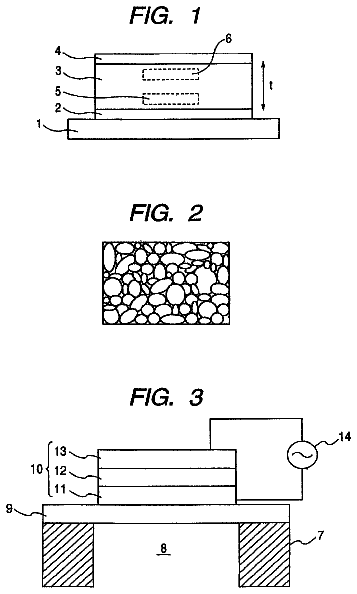
A heat generating component (3) is mounted on one surface of a circuit board (2).
US 8,715,791 B2 · Assignee: Renesas Electronics Corporation · Inventors: Tada; Munehiro et al.
Sheet 1 of 5 from the published document. All sheets in the USPTO PDF
A method for forming porous insulating film using cyclic siloxane raw material monomer, includes forming porous insulating film using the mixed gas of a cyclic organosiloxane raw material and a compound raw material including a part of chemical structure including the cyclic organosiloxane raw material. The compound raw material may include a compound including a part of side chain of the cyclic organosiloxane raw material.
In silicon semiconductor integrated circuit (LSI), conventionally, aluminum (Al) or Al alloy has been used extensively as the conductive material. With the recent advance in microfabrication technology used in the method for manufacturing of LSI, and for the purpose of reduction in resistance in the wiring and for improvement of reliability, use of copper (Cu) in the conductive material has begun to appear. Since Cu easily diffuses in a silicon oxide film, according to the prior art, conductive barrier metal film for prevention of diffusion of Cu is provided to side face and bottom face of the Cu wiring, and insulating barrier film is employed at top face of the Cu wiring. In recent years, progress in microfabrication of LSI resulted in wirings with finer dimensions, and increased capacity between wirings poses a problem, while introduction of porous low-dielectric constant film to inter
All 5 drawing sheets from the published document, cropped to the drawing.
What the patent claimed, word for word. All of it is now free to use.
The present invention relates to a method for forming porous insulating film, and in particular, relates to a semiconductor device including a wiring, and a semiconductor device including damascene wiring structure including Cu as principal component.
In silicon semiconductor integrated circuit (LSI), conventionally, aluminum (Al) or Al alloy has been used extensively as the conductive material. With the recent advance in microfabrication technology used in the method for manufacturing of LSI, and for the purpose of reduction in resistance in the wiring and for improvement of reliability, use of copper (Cu) in the conductive material has begun to appear. Since Cu easily diffuses in a silicon oxide film, according to the prior art, conductive barrier metal film for prevention of diffusion of Cu is provided to side face and bottom face of the Cu wiring, and insulating barrier film is employed at top face of the Cu wiring.
In recent years, progress in microfabrication of LSI resulted in wirings with finer dimensions, and increased capacity between wirings poses a problem, while introduction of porous low-dielectric constant film to interlayer insulating film has been accelerated. This is because employment of multilayer wiring to semiconductor elements allows high-speed and low-power connection, realization of low-dielectric constant features of interlayer insulating film as well as microfabrication are effective, and it is therefore necessary to meet with both requirements.
For the purpose of reduction in effective capacity between wirings, realization of low-dielectric constant features of interlayer insulating film (in this case, silicon oxide film (k=4.2)) is necessary. As low-dielectric constant film, for example, HSQ (Hydrogen Silsesquioxane) film, CDO (Carbon doped oxide) or organic film are included. These are formed by rotation coating method, vapor deposition method or the like.
Patent Document 1 discloses a technology of forming porous insulating film using plasma CVD method. Patent Document 2 describes a technology of forming porous insulating film using cyclic organosiloxane.
Patent Document 1: Japanese Patent Application Laid-Open No. 2004-289105
Patent Document 2: Japanese Patent Application National Publication No. 2002-526916
Problems to be Solved by the Invention
As described in the patent documents, according to the prior art, porous insulating film having specific inductive capacity of approximately 2.6 can be formed by the plasma CVD method using raw materials including cyclic organosiloxane. However, in accordance with microfabrication of LSI developed recently, necessity for a method for forming porous insulating films having specific inductive capacity 2.4 or less is cited, while forming by the plasma CVD method which ensures excellent adhesiveness is particularly desired. However, the prior art has the following drawbacks.
With the technology described in Patent Document 1, a film formation method of cutting-recombination type is used, in which raw material monomers are decomposed in plasma. For this reason, hydrocarbon components bound to raw material monomers are detached, and such a problem arises that reduction in specific inductive capacity is not possible, and limitation of reduction in specific inductive capacity is up to approximately 2.7.
Meanwhile, in the technology which uses cyclic siloxane raw material monomers described in Patent Document 2, cyclic structure of siloxane acts as the framework, specific inductive capacity of approximately 2.6 is obtained, steric hindrance is formed by having isopropyl group at side chain, additional reaction of the monomer is promoted by having vinyl group at side chain, whereby specific inductive capacity of approximately 2.5 can be obtained. However, even in this state, hydrocarbon amount in the film is smaller than that of raw material monomers, and for the purpose of further reduction in specific inductive capacity, a method, which further suppresses detachment of hydrocarbons, maintains framework of raw material siloxane as much as possible, and ensures formation of low-density film, is desired.
The purpose of the present invention is to provide a method for a forming porous insulating film using cyclic siloxane raw material monomers, that is, a method for a forming porous insulating film with reduced specific inductive capacity, and a semiconductor device including porous insulating film being formed by this method.
Means for Solving the Problems
The inventors of the present application investigated methods for a forming porous insulating film and found the above-mentioned method for a forming porous insulating film. The method for a forming porous insulating film of the present invention is characterized by that, in the method for forming insulating film by plasma vapor deposition method, in which at least cyclic organosiloxane raw material is supplied to a reaction chamber, a mixed gas of the cyclic organosiloxane raw material and a compound raw material containing a part of chemical structure comprising the cyclic organosiloxane raw material is used. In other words, energy flux of electrons in the plasma is reduced with the use of the gas in which cyclic organosiloxane raw material and the compound raw material are mixed, and an insulating film is formed while monomer structure of cyclic organosiloxane raw material is maintained. On this occasion, electrons in the plasma lose energy thereof through collision with compound raw materials, probability of destruction of cyclic organosiloxane raw material decreases, and porous insulating film can be formed while cyclic organosiloxane raw material is maintaining raw material structure thereof. In particular, presence of the compound raw material including chemical structure identical with that of the cyclic siloxane raw material in the reaction chamber enables suppression of decomposition of cyclic organosiloxane raw material.
In the meantime, while the mixed gas is in vaporized state, mixing ratio of the compound raw material with regard to 100% by volume of the cyclic organosiloxane raw material is preferably in a range from 5 to 200% by volume.
The method for forming porous insulating film according to the present invention is characterized by that the mixed gas is produced by vaporizing a mixed raw material of the cyclic organosiloxane raw material and the compound raw material. When a raw material, in which cyclic organosiloxane raw material and the compound raw material are mixed with arbitrary ratio, is used, cost reduction can be attained through a simplified film forming device, simplified film forming sequence, and stabilization.
Further, the compound raw material includes a part of side chain of the cyclic organosiloxane raw material. For this reason, if a side chain, that is a detachment component, is caused to be present in advance in the vapor phase, side chain bonding can be thermodynamically stabilized and detachment of side chain that is bonded to cyclic siloxane can be suppressed.
Cyclic organosiloxane raw material has a structure represented by Chemical formula
shown below, wherein R1 and R2 are preferably any one or more of methyl group, ethyl group, propyl group, isopropyl group, vinyl group, and allyl group, and specifically, a structure represented by Chemical formula (2), Chemical formula (3), or Chemical formula
shown below is preferable.
Alternatively, the compound raw material preferably includes a reaction precursor of the cyclic organosiloxane, or a compound, in which the compound raw material comprises at least silicon, oxygen, carbon, or hydrogen, having chemical structure represented by the following Chemical formula
may be used. Further, two or more of these the compound raw materials may be mixed.
In particular, the compound raw material is preferably at least either of methanol, ethanol, propanol, or isopropanol.
When the porous insulating film of the present invention is used as the interlayer insulating film being formed on a substrate on which semiconductor element is formed, low-capacity features between wirings are attained and at the same time, higher insulation reliability is obtained. Specifically, such a semiconductor device is meant that includes insulating film being formed by the plasma vapor deposition method, wherein at least cyclic organosiloxane raw material is supplied to the reaction chamber, which semiconductor device includes porous insulating film being formed by a mixed gas of the cyclic organosiloxane raw material and compound raw material containing a part of chemical structure comprising the cyclic organosiloxane raw material. Further, such a semiconductor device is meant that includes insulating film being formed by the plasma vapor deposition method, wherein at least cyclic organosiloxane raw material is supplied to the reaction chamber, which semiconductor device includes porous insulating film being formed by a mixed gas of the cyclic organosiloxane raw material and compound raw material containing a part of side chain of the cyclic organosiloxane raw material. Further, such a semiconductor device is meant that includes insulating film being formed by the plasma vapor deposition method, wherein at least cyclic organosiloxane raw material is supplied to the reaction chamber, which semiconductor device includes porous insulating film being formed using a mixed gas of the cyclic organosiloxane raw material and compound raw material that is a reaction precursor of the cyclic organosiloxane.
Novel features of the present invention will be better understood from the description of the specification and appended drawings.
Effect of the Invention
With the use of a method for forming porous insulating film and a semiconductor device according to the present invention, low-dielectric interlayer constant film is accomplished and eventually, performances of wirings are improved and formation of LSI with high-speed and low-power consumption features is made possible.
Before explaining the invention of the present application in greater detail, meanings of terms used herein will be explained.
Low-dielectric constant film denotes, for example, a film for separating wiring members by insulation (interlayer insulating film), and indicates a material with lower specific inductive capacity than silicon oxide film (specific inductive capacity: 4.2) used for the purpose of reduction in the capacity of multilayer wirings connecting semiconductor elements. Particularly, for porous insulating films, for example, material with lower specific inductive capacity (silicon oxide film is made porous), or materials with lower specific inductive capacity produced from HSQ (Hydrogen Silsesquioxane) film, or SiOCH, SiOC (e.g., Black Diamond (registered trademark), CORAL (registered trademark), Aurora (registered trademark)) by making them porous, are mentioned. At present, attainment of further lower dielectric constant of these films is desired.
In the present exemplary embodiment, metallic wiring materials are contained primarily of Cu. For the purpose of improvement of reliability of metallic wiring materials, metallic element other than Cu may be included in the material comprising Cu, or metallic element other than Cu may be formed on top face or side face of Cu.
Damascene wiring denotes a buried wiring produced in such that a metallic wiring material is buried in a groove of interlayer insulating film being formed in advance, and surplus metals other than the groove are removed by CMP or the like. Wiring structure normally employed when a damascene wiring is formed by Cu is such that side face and periphery of Cu wiring are covered by barrier metal, and top face of Cu wiring is covered by insulating barrier film.
CMP (Chemical Mechanical Polishing) method denotes such a method that concavity and convexity on wafer surface generated during multilayer wiring forming process are flattened by polishing by contacting the concavity and convexity to a rotating abrasive pad while abrasive liquid is introducing to the wafer surface. Particularly, in forming wirings by damascene method, this method is used to remove surplus metals after a metal is buried in the wiring groove or via hole and to obtain flat wiring surface.
Barrier metal denotes a conductive film including barrier features used for covering side face and bottom face of the wiring for prevention of diffusion of metallic element, that comprises the wiring, into interlayer insulation film or lower layer. For example, when a wiring comprises metallic elements composed primarily of Cu, high-melting point metals such as tantalum (Ta), tantalum nitride (TaN), titanium nitride (TiN), tungsten carbonitride (WCN), nitride thereof, or their laminated film are used.
Insulating barrier film is formed on top face of Cu wiring, has functions to prevent oxidation of Cu, or diffusion of Cu into insulating film, and acts as etching stop layer at processing. For example, SiC film, SiCN film, SiN film or the like are used.
Semiconductor substrate is a substrate on which is composed a semiconductor device, and includes SOI (Silicon on Insulator) substrate, TFT (Thin film transistor), or substrate for liquid crystal manufacturing, as well as those provided specifically on single crystal silicon substrate.
Hard mask denotes an insulating film which is laminated on the interlayer insulating film and plays a protection role, when performing CMP directly is difficult due to strength reduction by low-dielectric constant of the interlayer insulating film.
Passivation film is formed on the uppermost layer of a semiconductor element and has a role to protect the semiconductor element from moistures from the outside. In the present invention, silicon acid nitride film (SiON) formed by plasma CVD method, polyimide film, or the like are used.
The plasma CVD method is such a method that for example, raw material in gaseous state is supplied continuously to reaction chamber under reduced pressure, molecules are put into excitation state by plasma energy, and a continuous film is formed on a substrate by vapor phase reaction, or substrate surface reaction, or the like.
For PVD method, although ordinary sputtering method may be used, if improvement of burying characteristics, improvement of film quality, uniformity of film thickness in wafer plane are taken into considerations, sputtering method which ensures good directivity such as long throw sputtering method, collimate sputtering method, ionized sputtering method may also be used. When sputtering an alloy, a metal other than principal component is caused to be contained in advance in a metal target within solid solubility limit to obtain an alloy film from metal film being formed. In the present invention, this method may be used for forming Cu seed layer or forming barrier metal layer when damascene Cu-wiring is primarily formed.
TDDB (Time Dependent Dielectric Breakdown) service life is a method for predicting a time till occurrence of insulation destruction by accelerated test. For example, when TDDB service life of between wirings is measured, a comb type TEG (Test Element Group) is used, a comparatively high electric field of approximately from 1 to 4 MV/cm is applied under measurement conditions of a predetermined temperature (e.g., 125.degree. C.), and leakage current flowing between the wirings is monitored. Measurement of a time from electric field application start till insulation destruction allows comparison of superiority or inferiority of TDDB service life.
(Cyclic Organosiloxane Raw Material and Compound Raw Material)
The following description deals with cyclic organosiloxane raw material and compound raw material used in the method for a forming porous insulating film of the present invention.
Cyclic organosiloxane raw material is a compound represented by Chemical formula
shown previously. Alkyl group R1, R2 in Chemical formula
are methyl group, ethyl group, propyl group, isopropyl group, vinyl group, allyl group, or the like. Specifically, the cyclic organosiloxane raw material is preferably compound represented by Chemical formulae
to
shown previously.
Specifically, the compound raw material is preferably a compound including a part of chemical structure comprising the cyclic organosiloxane raw material, and a compound including side chain (alkyl group bound to Si, or the like) of the cyclic organosiloxane raw material is particularly preferable. For example, the cyclic organosiloxane raw material in Chemical formula
is a compound including each of alkyl groups R1, R2. The cyclic organosiloxane raw material in Chemical formula
is a compound including ethyl group and isopropyl group, the cyclic organosiloxane raw material in Chemical formula
is a compound including methyl group and isopropyl group, the cyclic organosiloxane raw material in Chemical formula
is a compound including vinyl group, isopropyl group, and propyl group or the like.
Compound materials may be alcohols in which alcohol group is bound to the compounds, and in particular, methanol, ethanol, propanol, isopropanol (IPA), or the like are mentioned. Further, compound raw materials may be alkane (methane series hydrocarbon), alkene (ethylene series hydrocarbon), alkine (acethylene series hydrocarbon) or the like in which H-- or further CH.sub.3-- or the like are bound to the compounds. Specifically, compound raw materials may be methan, ethan, propane, ethylene, acetylene, or the like. In addition, compound materials may be benzene, trimethylbenzene, naphthalene, or the like.
Further, the compound raw material is preferably a reaction precursor of the cyclic organosiloxane raw material. In other words, the cyclic organosiloxane is obtained by causing the reaction precursor to react. The reaction precursor of this cyclic organosiloxane raw material is a compound including a part of skeleton of the cyclic organosiloxane raw material and includes at least hydrogen, carbon, oxygen, silicon. The reaction precursor represented by above-mentioned Chemical formula
that is cyclic organosiloxane raw material is represented by above-mentioned Chemical formula (5), and therefore, if these cyclic organosiloxane raw materials and reaction precursor thereof are used as the mixed raw materials for forming of porous insulating film, forming of porous insulating film with lower dielectric constant becomes possible.
For above-shown compound raw material, one of above-mentioned compounds or two or more above-mentioned compounds may be used.
Although mixing ratio of cyclic organosiloxane raw material and compound raw material is not specifically limited, in a state where each of raw materials is vaporized, about 5 to 200% by volume of compound raw material with regard to 100% by volume of cyclic organosiloxane raw material is preferable. While a mixed gas of cyclic organosiloxane raw material and compound raw material is introduced to the reaction chamber (described later) for forming of porous insulating film, each of raw material gas of the cyclic organosiloxane raw material and compound raw material may be mixed in the reaction chamber, or liquid raw material being mixed in a step prior to the reaction chamber (mixed raw material) is vaporized by a vaporizer and mixed gas thus produced may be used, or raw materials vaporized in the step prior to the reaction chamber are mixed in the vaporizer and mixed gas thereof may be used.
(First Exemplary Embodiment)
In the present invention, in the method for forming porous insulating film preferable for interlayer insulating film by the plasma vapor deposition method while supplying at least cyclic organosiloxane raw material to reaction chamber, forming is made possible with the use of a mixed gas of cyclic organosiloxane raw material and compound raw material.
A first exemplary embodiment for forming porous insulating film while supplying a vaporized raw material supplied to a reaction chamber, will be explained hereunder referring to FIG. 1.
FIG. 1 is a schematic view showing one example of plasma CVD device which can be used for a forming porous insulating film (film forming) based on the method of the present invention. A plasma CVD device 50 shown in FIG. 1 includes a reaction chamber 10, a gas supplying section 20, a vacuum pump 30, and a high-frequency power supply 40. The gas supplying section 20 is connected to the reaction chamber 10 by a gas supplying pipe 22, and the vacuum pump 30 is connected to the reaction chamber 10 by a valve 32 and an exhaust pipe 36 with a cooling trap 34 mounted midway. The high-frequency power supply 40 is connected to the reaction chamber 10 by a high-frequency cable 44 with a matching box 42 mounted midway.
In the reaction chamber 10, a substrate heating section 3 which holds and heats a formed film member 1 such as semiconductor substrate, and a shower head 5 to which one end of the gas supplying pipe 22 is connected and which functions as gas blowing section are disposed each in opposed state. A ground wire 7 is connected to the substrate heating section 3, and the high-frequency cable 44 is connected to the shower head 5. Therefore, gas in a space between the substrate heating section 3 and the shower head 5 can be turned to plasma while raw material gas or the like is supplied from the gas supplying section 20 to the shower head 5 via the gas supplying pipe 22 and at the same time, high-frequency power generated by the high-frequency power supply 40 is supplied to the shower head 5 after a predetermined frequency is allocated thereto by a matching box 42 disposed along the way of the high-frequency cable 44.
The gas supplying section 20 includes raw material gas supply tanks as many as the number depending on the number of types of cyclic organosiloxane raw material gases to be used, supply tanks as many as the number depending on the number of types of compound raw materials to be used, gas supply tanks for carrier gas or dilution gas (hereafter referred to as "carrier gas supply tank"), and further includes a mixer 19 for mixing gases being supplied by each tank.
One end of the gas supplying pipe 22 is connected to the mixer 19. In FIG. 1 are shown one cyclic organosiloxane raw material gas supply tank 11, one compound raw material gas supply tank 13, and one carrier gas supply tank 15. The cyclic organosiloxane raw material gas supply tank 11 is connected to the mixer 19 by a piping 12, and the compound raw material gas supply tank 13 is connected to the mixer 19 by a piping 14, and the carrier gas supply tank 15 is connected to the mixer 19 by a piping 16. Two valves 18a, 18b and a gas flow rate control section 18 equipped with a gas flow rate controller 18c disposed between the valves 18a, 18b are provided in each of the piping of 12, 14, 16.
Meanwhile, a cleaning gas supplying pipe 28 to which are disposed a flow rate controller 24 and a valve 26 is connected to the gas supplying pipe 22 midway, and a waste fluid piping 38 is branched between the valve 32 in the gas exhaust pipe 36 and the cooling trap 34. It is preferable to provide a heater (not shown) for prevention of liquefaction of each gas in the transfer step around each of the piping 12, 14, 16 in the gas supplying section 20, and around gas supplying pipe 22, and these piping 12, 14, 16 or the gas supplying pipe 22 are preferably heated. Similarly, it is preferable to provide a heater (not shown) around the reaction chamber 10 for the purpose of heating of the reaction chamber 10.
In the method of forming organic silicon series film by the plasma CVD device 50, first, the formed film member 1 such as semiconductor substrate is disposed on the substrate heating section 3, the vacuum pump 30 is operated while the valve 32 is opened to attain initial vacuum degree in the reaction chamber 10 down to several Torr. Moisture in the gas exhausted from the reaction chamber 10 is removed by the cooling trap 34. Subsequently, raw material gas (gaseous cyclic organosiloxane gas) and compound gas are supplied from the gas supplying section 20 to the reaction chamber 10 together with carrier gas or dilution gas, and at the same time, the high-frequency power supply 40 and the matching box 42 are operated to supply high-frequency electric power at a predetermined frequency to the reaction chamber 10.
On this occasion, flow rate of each of gases is controlled by the corresponding flow rate controller 18, a mixed gas with a predetermined composition is generated by the mixer 19 and is supplied to the reaction chamber 10. Partial pressure of the raw material gas in the reaction chamber 10 is preferably selected appropriately within a range about from 0.1 to 3 Torr. Ambient pressure of the reaction chamber 10 at film forming is preferably set within a range about from 1 to 6 Torr by controlling the vacuum pump 30. Surface temperature of the formed film member 1 at film forming can be set appropriately within a range from 100 to 400.degree. C. by heating the formed film member 1 by the substrate heating section 3, and from 250 to 350.degree. C. is particularly preferable. As explained previously, compound raw material is supplied to the reaction chamber 10 prior to supplying of raw material gas, depending on the type thereof.
When film forming is carried out under such conditions, molecules of cyclic organosiloxane raw material that is a raw material gas are energized by plasma, reaching surface of the formed film member 1 in activated state, and porous insulating film is formed here. When the porous insulating film has a group with unsaturated bond, molecules of the organic silicon compound energized and then activated by plasma reach the surface of the formed film member 1, and receives further thermal energy from the substrate heating section 3, and therefore, the unsaturated bond in the above-mentioned group is ring-opened, thermal polymerization reaction proceeds among molecules, whereby porous insulating film is grown.
For cleaning of the reaction chamber 10, gases such as nitrogen trifluoride (NF.sub.3), sulfur hexafluoride (SF.sub.6), tetrafluoromethane (CF.sub.4), hexafluoroethane (C.sub.2F.sub.6) may be used, and these gases may be used, as necessary, as the mixed gas with oxygen gas, ozone gas, or the like. The cleaning gas is supplied to the reaction chamber 10 via the cleaning gas supplying pipe 28. In similar fashion as observed at film forming, high-frequency electric power is applied across the shower head 5 and the substrate heating section 3 to induce plasma, and cleaning of the reaction chamber 10 is carried out. Use of cleaning gas put in advance into plasma state with the use of remote plasma or the like is also effective.
(Second Exemplary Embodiment)
Hereafter, a second exemplary embodiment of the present invention, in which vaporized raw material is supplied to a reaction chamber to form porous insulating film, will be explained referring to FIG. 2. FIG. 2 is a schematic diagram showing one example of important part of a gas supplying section preferably used for a case where boiling point of cyclic organosiloxane intended to be used as the raw material gas is low, and the cyclic organosiloxane may become liquid state unless artificial heating is provided.
The cyclic organosiloxane raw material and compound raw material are mixed with arbitrary ratio, and the mixture is supplied from the gas supplying system 20 as mixed raw material 100.
A vaporization control unit VU includes a raw material tank 102 for accommodating the mixed raw material 100 in liquid state, a pressurized gas supplying device 106 for supplying pressurized gas into a raw material tank 102 via a pressurized gas supplying pipe 104, a mixed raw material transfer pipe 108 inserted one end thereof in the raw material tank 102, a liquid flow rate control section 110 provided in the middle of the mixed raw material transfer pipe 108, a vaporization section 112 disposed to other end of the mixed raw material transfer pipe 108. Above-mentioned liquid flow rate control section 110 includes two valves 110a, 110b, and a liquid flow rate control section 110c disposed between the valves 110a and 110b, and above-mentioned vaporization section 112 includes a valve 112a provided at above-mentioned other end side of the mixed raw material transfer pipe 108, and a vaporizer 112b connected to above-mentioned other end of the mixed raw material transfer pipe 108.
Further, each vaporization control units VU includes a gas supplying tank 114 for carrier gas or dilution gas (hereafter referred to as "carrier gas supplying tank 114"), a piping 116 for supplying the carrier gas or dilution gas in the carrier gas supplying tank 114 to the mixed raw material transfer pipe 108 at between the liquid flow rate control section 110 and a vaporization section 120. In the middle of the piping 116 is provided a gas flow rate control section 118 which includes two valves 118a, 118b, and a gas flow rate controller 118c being disposed between the valves 118a, 118b.
When a pressurized gas is supplied from the pressurized gas supplying device 106 into raw material tank 102 via the pressurized gas supplying pipe 104, internal pressure of the raw material tank 102 increases, the mixed raw material 100 in liquid state in the raw material tank 102 is transferred towards the vaporization section 112 via the mixed raw material transfer pipe 108, and reaches the vaporization section 112 while merging carrier gas or dilution gas on the way. The mixed raw material 100 in liquid state reached the vaporization section 112 is vaporized due to pressure reduction at introduction section of the vaporization section 112 and heating by a heater (not shown).
Use of such a vaporization system enables realization of uniform vaporization even with mixed raw materials.
A mixed gas generated by the vaporization control unit UV is sent to a gas exhaust pipe 120 which is connected to the vaporization section 112. The mixed gas then reaches a mixer 140 via a piping 124. When other raw material gas or additive gas or the like needs to be mixed further, mixing by the mixer 140 is possible.
From a viewpoint of smooth vaporization by each of vaporizers 112b, a heater is preferably provided around the mixed raw material transfer pipe 108 downstream from the valve 110c in the liquid flow rate control section 110, and the mixed raw material transfer pipe 108 is preferably heated. Similarly, for the purpose of prevention of liquefaction of each gas, a heater is preferably provided also around each gas exhaust pipes 120, 152, and the mixer 140 for heating them.
With the use of a film forming device including a gas supplying section comprising above-mentioned composition, desired porous insulating film can be obtained easily even a case where boiling point of a component comprising a mixed raw material intended to be used as the raw material gas is low, and the mixed raw material becomes liquid state unless artificial heating is provided.
(Third Exemplary Embodiment)
Hereafter, a third exemplary embodiment of the present invention, in which vaporized raw material is supplied to a reaction chamber to form porous insulating film, will be explained referring to FIG. 3. FIG. 3 is a schematic diagram showing one example of important part of the gas supplying section preferably used for a case where boiling point of cyclic organosiloxane intended to be used as the raw material gas is low, and the cyclic organosiloxane may become liquid state unless artificial heating is provided.
Cyclic organosiloxane raw material and compound raw material may be prepared in separate raw material tanks and mixed with arbitrary ratio each via a flow meter. Cyclic organosiloxane raw material 101 and compound raw material 103 are supplied from the raw material supplying system 20, respectively.
A vaporization control unit VU1 includes the raw material tank 102 for accommodating cyclic organosiloxane raw material 101 in liquid state, the pressurized gas supplying device 106 for supplying pressurized gas into the raw material tank 102 via the pressurized gas supplying pipe 104, the raw material transfer pipe 108 inserted one end thereof in the raw material tank 102, the liquid flow rate control section 110 provided in the middle of the raw material transfer pipe 108, the vaporization section 112 disposed to other end of the raw material transfer pipe 108. Above-mentioned liquid flow rate control section 110 includes two valves 110a, 110b, and the liquid flow rate controller 110c disposed between the valves 110a and 110b, and above-mentioned vaporization section 112 includes a valve 112a provided at above-mentioned other end side of the raw material transfer pipe 108, and a vaporizer 112b connected to above-mentioned other end of the raw material transfer pipe 108.
Further, each of vaporization control units VU1, VU1 includes the gas supplying tank 114 for carrier gas or dilution gas (hereafter referred to as "carrier gas supplying tank 114"), the piping 116 for supplying the carrier gas or dilution gas in the carrier gas supplying tank 114 to the raw material transfer pipe 108 at between the liquid flow rate control section 110 and vaporization section 120. In the middle of the piping 116 is provided the gas flow rate control section 118 which includes two valves 118a, 118b, and the gas flow rate controller 118c being disposed between the valves 118a, 118b.
With the vaporization control unit VU1, when a pressurized gas is supplied from the pressurized gas supplying device 106 into raw material tank 102 via the pressurized gas supplying pipe 104, internal pressure of the raw material tank 102 increases, the cyclic organosiloxane raw material 101 in liquid state in the raw material tank 102 is transferred towards the vaporization section 112 via the raw material transfer pipe 108, and reaches the vaporization section 112 while merging carrier gas or dilution gas on the way. The cyclic organosiloxane raw material 101 in liquid state reached the vaporization section 112 is vaporized due to pressure reduction at introduction section of the vaporization section 112 and heating by a heater (not shown).
Meanwhile, the vaporization control unit VU2 includes the raw material tank 102 for accommodating the compound raw material 103 in liquid state, the pressurized gas supplying device 106 for supplying pressurized gas into the raw material tank 102 via the pressurized gas supplying pipe 104, the raw material transfer pipe 108 inserted one end thereof in the raw material tank 102, the liquid flow rate control section 110 provided in the middle of the mixed raw material transfer pipe 108, the vaporization section 112 disposed to other end of the raw material transfer pipe 108.
Gasses generated by the vaporization control units VU1, VU2 are sent to the gas exhaust pipe 120 which is connected to the vaporization section 112. The gases then reach the mixer 140 via the piping 124 and are mixed.
From a viewpoint of smooth vaporization by each of vaporizers 112b, a heater is preferably provided around the raw material compound transfer pipe 108 downstream from the valve 110c in the liquid flow rate control section 110, and the raw material compound transfer pipe 108 is preferably heated. Similarly, for the purpose of prevention of liquefaction of each gas, a heater is preferably provided also around each of gas exhaust pipes 120, 152, and the mixer 140 for heating them.
With the use of a film forming device including a gas supplying section including above-mentioned composition, desired porous insulating film can be obtained easily even a case where boiling point of a raw material intended to be used as the raw material gas is low, and artificial heating is not provided.
As an example of the present invention, a case, where a raw material including chemical structure as represented by Formula
is used as the cyclic organosiloxane raw material, and isopropyl alcohol (IPA) is used as the compound raw material, will be described in greater detail. A plasma CVD device of parallel flat plate type as shown in the first exemplary embodiment was used as the film forming device, and a system for mixed raw material as shown in the second exemplary embodiment was used as a raw material system.
Cyclic organosiloxane raw material (Chemical Formula (4)) and IPA are mixed in advance with arbitrary ratio, and are supplied from the raw material supplying system to the reaction chamber as the mixed raw material. Heating temperature at the vaporizer can be set in a range from 80 to 120.degree. C. for the purpose of improvement of vaporization efficiency while suppressing thermal polymerization of raw material, and in this example, the temperature was set to 115.degree. C.
A plasma CVD device for 200 mm wafer was used, substrate temperature was 350.degree. C., distance between electrodes was set to 10 mm, and high-frequency electric power at 13.56 MHz was employed. Table 1 shows experimental conditions and results obtained from Examples 1, 2, Comparative example 1 where an insulating film is formed on the silicon substrate. Specific inductive capacity of the film was measured by a mercury probe, and C/Si ratio of the film was obtained by RBS.
It is confirmed that in Example 1 in which IPA was mixed, specific inductive capacity became smaller as compared to Comparative example 1 in which IPA was not mixed, and in Example 2 in which IPA ratio was high, specific inductive capacity became further smaller. It is considered that this finding is attributable to that detachment of isopropyl group being bound as the side chain of the cyclic organosiloxane raw material represented by Chemical Formula
was suppressed by mixing of IPA, thereby contributing to lower specific inductive capacity.
TABLE-US-00001 TABLE 1 Comparative example 1 Example 1 Example 2 Chemical Formula
65 65 65 IPA 0 5 35 Mixing ratio (%) 0 7 35 He (sccm) 300 300 300 RF (W) 100 100 100 Pressure (Torr) 2.7 2.7 2.7 Specific inductive capacity 2.45 2.42 2.35 C/Si ratio in film 3.17 3.2 3.25
As an example of the present invention, a case, where raw material including chemical structure represented by Chemical Formula
is used as the cyclic organosiloxane raw material, and one represented by Chemical Formula
is used as the compound raw material, will be described in greater detail. A plasma CVD device of parallel flat plate type as shown in the first exemplary embodiment was used as the film forming device, and a system for mixed raw material as shown in the second exemplary embodiment was used as the raw material supplying system.
Cyclic organosiloxane raw material (Chemical Formula (4)) and compound raw material (Chemical Formula (5)) are mixed in advance with arbitrary ratio, and are supplied from the raw material supplying system as the mixed raw material. Heating temperature at the vaporizer can be set in a range from 80 to 120.degree. C. for the purpose of improvement of vaporization efficiency while suppressing thermal polymerization of raw material, and in this example, the temperature is set to 115.degree. C. Since the compound raw material (Chemical Formula (5)) contains smaller number of vinyl groups as compared to cyclic organosiloxane raw material (Chemical Formula (4)), polymerization is hardly promoted at higher temperature, and a large quantity of compound raw materials can be supplied easily to the reaction chamber.
A plasma CVD device for 200 mm wafer was used, substrate temperature was 350.degree. C., distance between substances was set to 14 mm, and high-frequency electric power at 13.56 MHz was employed. Table 2 shows experimental conditions and results obtained from Examples 3, 4, Comparative example 2 where an insulating film is formed on the silicon substrate.
The description continues in the full USPTO document.
About 6,378 words. The USPTO PDF has it with every drawing.
Fees are due 3.5, 7.5 and 11.5 years after grant. This patent expired on May 6, 2026, so the fee marked "not paid" was the one that went unpaid.
Method for Forming Porous Insulating Film and Semiconductor Device
Filed Sep 2006 · published Sep 2010Method for forming porous insulating film and semiconductor device
Filed Sep 2006 · granted May 2014Earlier publications, parents and continuations. None of them can still be enforced, or this patent would not be listed.
Prior art cited by the examiner or applicant. Useful when you check your own idea for novelty.
Everything on this page comes from the documents linked above.