 Lapsed, fee not paid7 drawings
Software & Apps · US 8,713,485 B2
Categorization of design rule errors
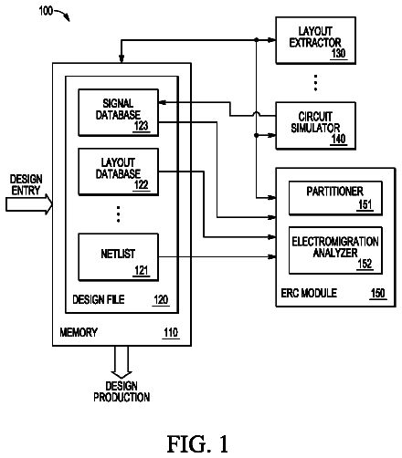
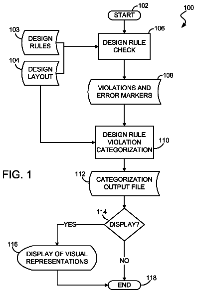
Embodiments of the invention include a method for categorizing and displaying design rule errors.
US 8,713,503 B2 · Assignee: Fujitsu Limited · Inventors: Ishikawa; Yoichiro
Sheet 1 of 15 from the published document. All sheets in the USPTO PDF
A design assisting apparatus includes a memory configured to store routing information representing first wire line from wire lines of a module belonging to a first layer of a semiconductor circuit having a plurality of layers, the first wire line likely to become either one of an aggressor net and a victim net in a crosstalk noise check performed on wire lines of a module belonging to a second layer hierarchically higher than the first layer, and a processor configured to perform a wire line identifying operation identifying second wire line within the module belonging to the second layer, and likely to become either one of an aggressor net and a victim net in the crosstalk noise check performed on the first wire line represented by the routing information stored on the memory.
According to one of the related-art layout design methods of semiconductor integrated circuit such as large scale integration (LSI), a circuit partitioned into a plurality of blocks by function is hierarchically layered and then layout-designed on a per layer basis. Design data are then collected to perform the whole system design. A crosstalk noise check is typically performed in parallel with the layout design. In a typical method, for example, a layout is designed while a noise check is performed to make sure that no crosstalk noise is generated. All layers are expanded with the layout of the entire semiconductor circuit completed (all the placing and routing completed), and the crosstalk noise check is performed on all the wire lines. A designer may perform a variety of layout designs to make sure that no crosstalk noise is generated in a layer design phase. For example, line spacing
1 of 15 drawing sheets so far from the published document, cropped to the drawing. Every sheet is in the USPTO PDF.
What the patent claimed, word for word. All of it is now free to use.
This application is based upon and claims the benefit of priority of the prior Japanese Patent Application No. 2010-253347, filed on Nov. 12, 2010, the entire contents of which are incorporated herein by reference.
The embodiments discussed herein are related to a design assisting apparatus, method, and program.
According to one of the related-art layout design methods of semiconductor integrated circuit such as large scale integration (LSI), a circuit partitioned into a plurality of blocks by function is hierarchically layered and then layout-designed on a per layer basis. Design data are then collected to perform the whole system design.
A crosstalk noise check is typically performed in parallel with the layout design. In a typical method, for example, a layout is designed while a noise check is performed to make sure that no crosstalk noise is generated. All layers are expanded with the layout of the entire semiconductor circuit completed (all the placing and routing completed), and the crosstalk noise check is performed on all the wire lines.
A designer may perform a variety of layout designs to make sure that no crosstalk noise is generated in a layer design phase. For example, line spacing is widened such that no effect is caused by another wire line. For shielding purposes, a ground wire line may be interposed between wire lines presenting a problem.
In another known method, a driving power of an aggressor wire line or a victim wire line is adjusted in the layer layout phase. In yet another method, crosstalk noise is prevented from being generated on a hierarchically high layer by arranging a wiring inhibit area beforehand within a hierarchically low layer.
In addition to the above layout methods, the following methods are also available. In one method, check results of a hierarchically low layer are organized in a library and then added to the check results of a hierarchically high layer in the checking of a net linking the hierarchically low layer to the hierarchically high layer. In another method, lengths of parallel running wire lines in layers are summed. If the sum of the wire lines exceeds a reference line length, an error is suspected, and a crosstalk location is thus identified.
Related arts are described in Japanese Laid-open Patent Publication No. 2005-63275, Japanese Laid-open Patent Publication No. 2002-270775, Japanese Laid-open Patent Publication No. 2003-44540, Japanese Laid-open Patent Publication No. 2001-217315, and Japanese Laid-open Patent Publication No. 2004-185374.
The method of expanding all the layers with the layout of the entire semiconductor circuit completed, and performing the crosstalk noise check on all the wire lines has the problem discussed below. A data size greatly increases as the number of layers increases, and a memory used in a computer is occupied by data of the wire lines. The calculation speed of the computer is reduced.
Even if the crosstalk noise is controlled as much as possible by improving the layout design, the layout of a block at a layer level may remain pending in the layer design. For example, in the layout of a particular block, a driver driving power may remain unknown, a wire line extending to another layer may be present, wire lines in the vicinity of a boundary may include one extending to a driver or a receiver, and the effect of a wire line on an adjacent block is unknown. In such a case, the crosstalk noise is difficult to check correctly.
The method of widening the line spacing and the shielding method of interposing the ground wire line between the problematic wire lines are also associated with an inefficient layout problem such as an introduction of a dead space in the semiconductor circuit and an increase in a die size.
The layout constraint is imposed as described above to perform the crosstalk noise check correctly, and the crosstalk noise is also reduced. Such a method has a limited effect in current LSIs.
The check results of the hierarchically low layer are organized in the library and then added to the check results of the hierarchically high layer. With this method, however, the checking of the crosstalk noise is difficult because a wire line passing above and a wire line adjacent to a boundary in the hierarchically low layer are not accounted for.
In the method, the lengths of parallel running wire lines in layers are summed. If the sum of the wire lines exceeds a reference line length, an error is suspected, and a crosstalk location is identified. The summing of the lengths of the parallel running wire lines alone leads no correct crosstalk noise check. The checking of the crosstalk noise is difficult because the wire line passing above the low layer and the wire line adjacent to the boundary in the hierarchically low layer are not accounted for. With this method, the crosstalk noise check is not correctly performed.
A design assisting apparatus includes a memory configured to store routing information representing first wire line from wire lines of a module belonging to a first layer of a semiconductor circuit having a plurality of layers, the first wire line likely to become either one of an aggressor net and a victim net in a crosstalk noise check performed on wire lines of a module belonging to a second layer hierarchically higher than the first layer, and a processor configured to perform a wire line identifying operation identifying second wire line within the module belonging to the second layer, and likely to become either one of an aggressor net and a victim net in the crosstalk noise check performed on the first wire line represented by the routing information stored on the memory.
The object and advantages of the invention will be realized and attained at least by the elements, features, and combinations particularly pointed out in the claims.
It is to be understood that both the foregoing general description and the following detailed description are exemplary and explanatory and are not restrictive of the invention, as claimed.
FIG. 1 generally illustrates a design assisting apparatus of a first embodiment;
FIG. 2 illustrates a process flow of LSI design;
FIG. 3 illustrates a hardware structure of a design assisting apparatus of a second embodiment;
FIG. 4 is a functional block diagram of the design assisting apparatus;
FIG. 5 illustrates a structure of a main-chip database (DB);
FIG. 6 illustrates a calculation method of a crosstalk noise value;
FIG. 7 is a functional block diagram of a sub-chip processor;
FIG. 8 is a flowchart of a check process of the crosstalk noise;
FIG. 9 is a flowchart illustrating a process of a sub-chip processor;
FIG. 10 illustrates layers of an LSI;
FIG. 11 illustrates information written in an interface file, and routing error information written in a result file;
FIG. 12 illustrates a process of the sub-chip processor generating the interface file and the result file;
FIG. 13 illustrates a generation of the interface file and the result file;
FIG. 14 illustrates the layers of the LSI; and
FIG. 15 illustrates a crosstalk noise check of a main chip.
First Embodiment
FIG. 1 generally illustrates a design assisting apparatus 1 of a first embodiment.
The design assisting apparatus 1 of FIG. 1 is used to perform a layout design of a semiconductor circuit having a plurality of layers.
FIG. 1 illustrates as a design target a semiconductor integrated circuit model 2 having a plurality of layers. The semiconductor integrated circuit model 2 includes three layers. The semiconductor integrated circuit model 2 is partitioned and placed by functional block. In the discussion of the first embodiment, each block is referred to as a module.
The semiconductor integrated circuit model 2 includes a module 2a on a hierarchically top layer (layer A). The module 2a includes two modules 2b and 2c belonging to a layer (layer B) lower than the topmost layer by one layer. The module 2b includes a module 2d belonging to a layer (layer C) lower than the topmost layer by two layers. The module 2c includes a module 2e belonging to the layer C.
The design assisting apparatus (for example, a computer) 1 of the embodiment includes memories 1a1, 1a2, 1a3, and 1a4, and line identifying unit 1b.
The memory 1a1 stores routing information related to a wire line likely to become an aggressor net (net giving a crosstalk effect) or a victim net (net receiving a crosstalk effect), from the wire lines of the module belonging to the first layer of the semiconductor integrated circuit model 2, with respect to a wire line of a module belonging to the second layer as any layer hierarchically higher than the first layer.
In the discussion that follows, the first layer is set as the layer C as the bottommost layer. In this case, the second layer includes the layer A and the layer B.
The memory 1a1 stores routing information D1 related to a wire line L1 likely to become an aggressor net or a victim net, from wire lines L1, L4, and L5 of the module 2d belonging to the layer C, to a wire line L2 of the module 2b belonging the layer B and a wire line L3 of the module 2a belonging to the layer A.
The routing information D1 may be generated by a routing information generating unit 1c. The routing information generating unit 1c extracts a wire line likely to become one of an aggressor net and a victim net, output of the wire lines L1, L4, and L5 of the module 2d, to the wire line L2 of the module 2b and the wire line L3 of the module 2a. As a result of extraction, the routing information generating unit 1c determines that the wire line L1 is likely to be one of the aggressor net and the victim net to the wire line L2 and the wire line L3, and generates the routing information D1. The routing information generating unit 1c also determines the wire lines L4 and L5 are not likely to become either one of the aggressor net and the victim net to the wire lines of the module 2b and the module 2a. The determination rule is discussed with reference to a second embodiment.
In the generation of the routing information D1, the routing information generating unit 1c excludes the wire line L6 of the module 2e and the wire line L7 of the module 2c as the target of the routing information D1. More specifically, the routing information generating unit 1c generates the routing information with the modules 2a, 2b, and 2d treated as one process unit, and the modules 2a, 2c, and 2e treated as one process unit. In this way, an amount of calculation in the generation of the routing information is reduced.
After generating the routing information D1, the routing information generating unit 1c sets the first layer at the layer B higher than the layer C by one layer, and generates routing information of the module 2b belonging to the layer B. The second layer becomes the layer A at the topmost layer. More specifically, the routing information generating unit 1c extracts a wire line likely to become either one of the aggressor net and the victim net, i.e., the wire line L2 of the module 2b, to the wire line L3 of the module 2a. Through the extraction operation, the routing information generating unit 1c determines that the wire line L2 is likely to be one of the aggressor net and the victim net to the wire line L3, and generates the routing information D2 related to the wire line L2. The routing information generating unit 1c then stores the generated routing information D2 on the memory 1a2.
The routing information generating unit 1c has generated the routing information of the modules 2a, 2b, and 2d as the process unit. The routing information generating unit 1c then generates the routing information of the module 2a, 2c, and 2e as the process unit. After generating the routing information D2, the routing information generating unit 1c sets the first layer at the layer C as the bottommost layer again, and generate the routing information of the module 2e belonging to the layer C. More specifically, the routing information generating unit 1c extracts a wire line likely to become either one of the aggressor net and the victim net, i.e., the wire line L6 of the module 2e, to the wire line L7 of the module 2c and the wire line L3 of the module 2a. Through the extraction operation, the routing information generating unit 1c determines that the wire line L6 is likely to be either one of the aggressor net and the victim net to the wire line L7, and generates the routing information D3 related to the wire line L6. The routing information generating unit 1c then stores the generated routing information D3 on the memory 1a3.
After generating the routing information D3, the routing information generating unit 1c sets the first layer at the layer B higher than the layer C as the bottommost layer by one layer, and generate the routing information of the module 2c belonging to the layer B. More specifically, the routing information generating unit 1c extracts a wire line likely to become either one of the aggressor net and the victim net, i.e., the wire line L7 of the module 2c, to the wire line L3 of the module 2a. Through the extraction operation, the routing information generating unit 1c determines that the wire line L7 is likely to be either one of the aggressor net and the victim net to the wire line L3, and generates the routing information D4 related to the wire line L7. The routing information generating unit 1c then stores the generated routing information D4 on the memory 1a4.
The line identifying unit 1b then identifies a wire line eligible for a crosstalk noise calculation. More specifically, the line identifying unit 1b identifies a wire line within a module belonging to the second layer, and likely to become either one of the aggressor net and the victim net to the wire lines of the routing information D1-D4 stored on the memories 1a1-1a4. The line identifying unit 1b, when identifying a wire line eligible for a crosstalk noise calculation on a module at a given layer, identifies a wire line becoming either one of the aggressor net and the victim net to the wire lines of the routing information of all the modules belonging to the layer lower than the given layer.
The line identifying unit 1b may identify on the module 2b a wire line eligible for the crosstalk noise calculation. More specifically, the line identifying unit 1b identifies a wire line within the module 2b (unconnected to an upper layer), i.e., the wire line L2 likely to become either one of the aggressor net and the victim net to the wire line L1 of the routing information D1. Through the identification operation, the crosstalk noise value with the wire line L1 being the aggressor net and the wire line L2 being the victim net is ready to be calculated. The crosstalk noise value with the wire line L1 being the victim net and the wire line L2 being the aggressor net is ready to be calculated.
The line identifying unit 1b, when identifying a wire line eligible for the crosstalk noise calculation on the module 2c, identifies a wire line within the module 2c, i.e., the wire line L7 likely to become either one of the aggressor net and the victim net to the wire line L6 of the routing information D3. Through the identification operation, the crosstalk noise value with the wire line L6 being the aggressor net and the wire line L7 being the victim net is ready to be calculated. The crosstalk noise value with the wire line L6 being the victim net and the wire line L7 being the aggressor net is ready to be calculated.
The line identifying unit 1b, when identifying a wire line eligible for the crosstalk noise calculation on the module 2a, identifies a wire line within the module 2a, i.e., the wire line L3 likely to become either one of the aggressor net and the victim net to the wire lines L2 and L7 of the routing information D2 and D4. Through the identification operation, the crosstalk noise values with the wire lines L2 and L7 being the aggressor nets and the wire line L3 being the victim net are ready to be calculated. The crosstalk noise values with the wire lines L2 and L7 being the victim nets and the wire line L3 being the aggressor net are ready to be calculated.
The design assisting apparatus 1 of the embodiment further includes a crosstalk noise verifier 1d verifying the crosstalk noise of the semiconductor integrated circuit model 2 in accordance with the identification results of the line identifying unit 1b.
As illustrated in FIG. 1, the crosstalk noise verifier 1d calculates the crosstalk noise value with the wire line L1 being the aggressor net and the wire line L2 being the victim net. The crosstalk noise verifier 1d also calculates the crosstalk noise value with the wire line L1 being the victim net and the wire line L2 being the aggressor net. Similarly, the crosstalk noise verifier 1d calculates the crosstalk noise value with the wire line L6 being the aggressor net and the wire line L7 being the victim net. The crosstalk noise verifier 1d also calculates the crosstalk noise value with the wire line L6 being the victim net and the wire line L7 being the aggressor net. The crosstalk noise verifier 1d calculates the crosstalk noise values with the wire lines L2 and L7 being the aggressor net and the wire line L3 being the victim net. The crosstalk noise verifier 1d also calculates the crosstalk noise value with the wire line L2 and L7 being the victim net and the wire line L3 being the aggressor net.
If the calculated crosstalk noise value is equal to or higher than a constant value, the crosstalk noise verifier 1d determines that the calculated crosstalk noise value is an error verification. The crosstalk noise verifier 1d then outputs a combination of the wire lines L1 and L2 to the accumulator 1e as an error result. As illustrated in FIG. 1, an error result E1 is stored on the accumulator 1e. The error result E1 indicates that the crosstalk noise value with the wire line L1 being the aggressor net and the wire line L2 being the victim net is the error verification.
The routing information generating unit 1c may retrieve combination information indicating a combination of the wire lines L4 and L5 that permits the calculation of the crosstalk noise value to be completed within the module 2b, and may store the combination information on a memory 1f. In such a case, the crosstalk noise verifier 1d verifies the crosstalk noise value of the combination of the wire lines L4 and L5 stored on the memory 1f. If the verification results indicate that the crosstalk noise value is equal to or higher than the constant value, the crosstalk noise value is determined as an error verification. The combination of the wire lines L4 and L5 is output to an accumulator 1e as an error result E2.
The design assisting apparatus 1 calculates the crosstalk noise between a wire line identified by the line identifying unit 1b as being likely to become either one of the aggressor net and the victim net and a wire line likely to become either one of the aggressor net and the victim net stored on the memories 1a1 through 1a4. The crosstalk noise value may be calculated at each layer. A memory having a small memory capacity may be used to calculate the noise. The verification of the crosstalk noise is performed at a high speed. A high-accuracy crosstalk noise verification is performed without the need for expanding all layers at a time.
The line identifying unit 1b, the routing information generating unit 1c, and the crosstalk noise verifier 1d may be implemented using a function of a central processing unit (CPU) of the design assisting apparatus 1. The memories 1a1, 1a2, 1a3, 1a4, and 1f and the accumulator 1e may be implemented using a data storage area of a random-access memory (RAM) or a hard disc drive (HDD) of the design assisting apparatus 1.
Second Embodiment
A design assisting apparatus 10 of a second embodiment performs a layout design of a semiconductor integrated circuit having a plurality of layers. In the discussion that follows, the semiconductor integrated circuit is an LSI.
FIG. 2 illustrates an example of process flow of LSI design.
S1 Using a specific architecture performing a desired function, a designer designs an LSI in accordance with register transfer level (RTL) description referred to as Verilog hardware description language (HDL) or VHDL (VHSIC HDL). This design is referred to as RTL design, and is a first operation of the process flow of the LSI design. Behavioral design may occasionally be performed in advance using a behavior model. For simplicity of explanation, such a behavioral design is not discussed here.
In the RTL design phase, the RTL described LSI is logically verified and the RTL description is improved until the circuit is free from any problem. Such an operation is omitted in FIG. 2.
S2 Logic synthesis is then performed when the RTL design is complete. The logic synthesis is performed to generate a net list from the RTL design. The net list is circuit information of a circuit constructed of real circuit elements. In the logic synthesis, a condition of synthesis constraints such an appropriate timing constraint is set, and the logic synthesis is performed such that the circuit of the generated net list operates at a desired operation frequency. The logic synthesis is followed by the layout design in S3 and subsequent operations performed in accordance with the generated net list.
S3 The designer creates a floor plan that determines an approximate location of each module forming a major LSI. In the floor plan, each module to be layout-processed is hierarchically partitioned, and where to place the partitioned module within a layout area is then determined. In the hierarchically partitioned module at a hierarchically low layer is referred to as a "sub chip." Through the hierarchically partitioning, the crosstalk estimation within the sub chip in S5 to be discussed later is performed separately. Processing proceeds to S4.
S4 Subsequent to the hierarchically partitioning, design is performed on the hierarchically partitioned sub chips on a per sub-chip basis. In the design of each sub chip, the designer places and routes cells using the design assisting apparatus 10. Processing proceeds to S5.
S5 The designer issues to the design assisting apparatus 10 an instruction to perform a crosstalk noise check on results of actual routing on a per sub chip basis. Processing proceeds to S6. FIG. 2 illustrates the crosstalk noise check with a layout verification and a timing verification omitted.
S6 The design assisting apparatus 10 performs the crosstalk noise check, and the designer may receive from the design assisting apparatus 10 a notification to the effect that an error is present (yes from S6). Processing returns to S4, and the designer reviews the cell placement and routing. If the designer receives from the design assisting apparatus 10 a notification to the effect that no error is present (no from S6), processing proceeds to S7.
The designer continues to review the placement and routing on a per sub-chip basis until no error is detected in the crosstalk noise check.
S7 The designer completes sub-chip design. After the crosstalk noise check is successfully completed on a per sub-chip basis, the designer then performs a system design of the LSI. In the system design of the LSI, the designer performs a placement and routing process on an upper layer including the sub chips. A main-chip database (DB) and a sub-chip DB are generated in the system design. The generated main-chip DB and sub-chip DB are stored on a storage device of the design assisting apparatus 10.
S8 Upon completing the system design, the designer performs the crosstalk noise check. The crosstalk noise check in S8 includes checking the crosstalk noise between layers.
More specifically, the designer issues a crosstalk noise check instruction to the design assisting apparatus 10 when the sub-chip design is partially or entirely complete. The design assisting apparatus 10 performs the crosstalk noise check on a sub chip as a block box if the sub chip is not completed in design.
S9 If the results of the crosstalk noise check of the design assisting apparatus 10 indicate that an error is present in the whole LSI (yes from S9), processing returns to S4 to review the design of each sub chip. If no error is present in the whole LSI (no from S9), processing proceeds to S10.
S10 The designer generates manufacturing data for the LSI when the whole LSI has no longer any error in the crosstalk noise check. The designer thus completes the circuit design, and proceeds to the manufacturing phase of the LSI.
The crosstalk noise check in S5 may be omitted. In such a case, the crosstalk noise check of each sub chip is performed in S8.
The design assisting apparatus 10 thus designs the sub chip and performs the crosstalk noise check on the entire chip. A hardware configuration and function of the design assisting apparatus 10 are described below in detail.
FIG. 3 illustrates the hardware configuration of a design assisting apparatus 10 of the second embodiment. The design assisting apparatus 10 is generally controlled by a CPU 101. The CPU 101 is connected to a RAM 102 and a plurality of peripheral devices via a bus 108.
The RAM 102 is used as a main storage device of the design assisting apparatus 10. The RAM 102 temporarily stores at least part of an operating system (OS) to be executed by the CPU 101 and application programs. The RAM 102 also stores a variety of data used by the CPU 101.
The peripheral devices connected to the bus 108 include HDD 103, graphic processor device 104, input interface 105, optical drive device 106, and communication interface 107.
The HDD 103 writes and reads data on an internal disc magnetically. The HDD 103 is used as an auxiliary storage device of the design assisting apparatus 10. The HDD 103 stores the OS, the application programs, and the variety of data. A semiconductor memory such as a flash memory may also be used as the auxiliary storage device.
The graphic processor device 104 is connected to the monitor 104a. In response to an instruction from the CPU 101, the graphic processor device 104 causes an image to be displayed on the monitor 104a. The monitor 104a may be a cathode ray tube (CRT) display device or a liquid-crystal display device.
The input interface 105 is connected to a keyboard 105a and a mouse 105b. The input interface 105 transfers signals from the keyboard 105a and the mouse 105b to the CPU 101. The mouse 105b is one example of pointing devices. Another pointing device may also be used. The other pointing devices include, for example, a touchpanel, tablet, touchpad, and trackball.
The optical drive device 106 reads data, recorded on an optical disc 200, using laser light. The optical disc 200 is a portable recording medium having data recorded thereon and readable through light reflection. For example, the optical disc 200 may be Blu-ray disc (registered trademark), digital versatile disc (DVD), DVD-RAM, compact disc read-only memory (CD-ROM), compact disc recordable (CD-R), compact disc rewritable (CD-RW), or the like.
The communication interface 107 is connected to a network 50. The communication interface 107 exchanges data with another computer or a communication apparatus via the network 50.
Functions of the design assisting apparatus 10 of the embodiment are thus performed on the above-described hardware configuration. The functions of the design assisting apparatus 10 having the hardware configuration are described below.
FIG. 4 is a functional block diagram of the design assisting apparatus 10.
The design assisting apparatus 10 includes sub-chip list generator 11, sub-chip processor 12, layout data reading unit 13, interface file reading unit 14, check data generator 15, crosstalk noise value calculator 16, crosstalk noise value determiner 17, result file generator 18, all result file reading unit 19, error list generator 20, main-chip DB storage unit 21, sub-chip DB storage unit 22, interface file storage unit 23, and result file storage unit 24.
The sub-chip list generator 11 generates a list of sub chips in accordance with a main-chip DB stored on the main-chip DB storage unit 21. The main-chip DB stores the layout data of the whole LSI.
FIG. 5 illustrates a structure of the main-chip DB.
The floor plan and the hierarchical partitioning result in circuit blocks of four layers as illustrated in FIG. 5.
The sub chips belonging to the bottommost layer (fourth layer) of an LSI 30 include a sub chip 31 and a sub chip 32. The sub chip 31 and the result file storage unit 24 are parallel to each other. If viewed from the sub chip 31, the sub chip belonging to a third layer right above the sub chip 31 is a sub chip 33. The sub chip belonging to a second layer right above the sub chip 33 is a sub chip 34. A first layer as the topmost layer is a main chip 30a.
The second layer of the LSI 30 also includes sub chips 35, 36, and 37 in addition to the sub chip 34. The sub chips 34-37 are in a parallel relationship to each other at the second layer.
The sub chips 35 and 36 include hierarchically lower sub chips, respectively, and the sub chip 37 includes no hierarchically lower sub chip. As illustrated in FIG. 5, the sub chips 35-37 are illustrated as black boxes.
The main chip 30a and the sub chips 31-37 have undergone the routing process. For example, wire lines L11 are arranged on the sub chip 31, and wire lines L12 and L13 are arranged on the sub chip 33. A wire line L14 is arranged on the sub chip 34. Wire lines L15, L16, and L17 are arranged on the main chip 30a.
The sub-chip processor 12 expands the bottommost layer to the upper layer right above the bottommost layer in order, and performs the crosstalk noise check on all the layers when all the sub chips are laid out or when a particular sub chip regardless of the bottommost layer or the upper layer is laid out. For example, the layout data reading unit 13 expands the sub chip 31 and the immediately upper layers on the LSI 30 of FIG. 5, thereby viewing the sub chips 31, 33, 34, and the main chip 30a in a flat state. The sub-chip processor 12 thus performs the crosstalk noise check on all these layers.
The sub-chip processor 12 then stores, in an interface file, information related to a wire line having a crosstalk noise value unfixed on each sub chip with respect to one of the upper sub chips including the main chip 30a. The information is hereinafter referred to as pending routing information. The rule of the wire line providing the pending routing information is described below in detail. The sub-chip processor 12 stores the interface file on the interface file storage unit 23. The interface file is generated on a per sub chip basis.
The crosstalk noise check is performed on a region of each sub chip where the layout has been complete. If the crosstalk noise check results in an error, information of a wire line pair resulting in the error (routing error information) is written in a result file. The sub-chip processor 12 stores the result file on the result file storage unit 24. The result file is generated on a per sub chip basis.
The design assisting apparatus 10 is continuously discussed with reference to FIG. 4.
The layout data reading unit 13 reads layout data of a layout (layout position) of each sub chip of the LSI 30. The layout data reading unit 13 may read the layout data from the main-chip DB or receive the layout data read by the sub-chip list generator 11.
The interface file reading unit 14 reads an interface file of a sub chip belonging to the second layer stored on the interface file storage unit 23.
In accordance with the interface file read by the interface file reading unit 14, the check data generator 15 checks the line spacing between lines to determine whether the line pair is a target of the crosstalk noise check. The check data generator 15 thus generates data of the crosstalk noise check (check data) according to which the line pair having a line spacing equal to or smaller than a constant value is set to be a crosstalk noise check target.
The crosstalk noise value calculator 16 calculates the crosstalk noise value between wire lines using the check data generated by the check data generator 15.
FIG. 6 illustrates an example of the calculation method of the crosstalk noise value.
As illustrated in FIG. 6, a wire line L21 between a driver cell D1 and a receiver cell R1 is specified to be a victim net through crosstalk. A wire line L22 between a driver cell D2 and a receiver cell R2 and a wire line L23 between a driver cell D3 and a receiver cell R3 are specified to be aggressor nets, respectively.
As illustrated in FIG. 6, the crosstalk noise value calculator 16 calculates the crosstalk noise value of the wire line L21 with the wire line L22 along segments A1 and A2 where the line spacing between the wire line L21 and the wire line L22 is equal to or smaller than a specific value. The crosstalk noise value calculator 16 also calculates the crosstalk noise value of the wire line L23 with the wire line L21 along a segment A3 where the line spacing between the wire line L21 and the wire line L23 is equal to or smaller than the specific value.
In the crosstalk noise calculation, the crosstalk noise value calculator 16 performs a 1:1 noise value calculation with the ratio of the victim net to the aggressor net being 1:1, and performs a 1:2 noise value calculation with the ratio of the victim net to the aggressor net being 1:2. As illustrated in FIG. 6, the 1:1 noise value calculation is performed on each of the segment A1 between the wire line L21 and the wire line L22, the segment A2 between the wire line L21 and the wire line L22, and the segment A3 between the wire line L21 and the wire line L23. The 1:1 noise values are thus calculated between the wire line L21 and the wire line L22, and between the wire line L21 and the wire line L23. The 1:2 noise value is calculated from the 1:1 noise values between the wire line L21 and each of the wire line L22 and the wire line L23.
The calculation of a 1:1 noise value Nv11 is represented by Equation (1): Nv11=.SIGMA.{Ln.times.Ka.times.f(C,L)}.ltoreq.LX1
where Ln represents a length of a line segment where a particular net runs in parallel with a victim net side by side. As illustrated in FIG. 6, Ln is the length of each of the segments A1-A3. Ka represents a coefficient of a driver driving power between the victim net and the aggressor net. f(C,L) represents a relaxation function and is determined by a distance between the victim net and the aggressor net. LX1 represents a limitation value to the 1:1 noise, and is determined by a type-based combination of the victim net and the aggressor net.
A 1:2 noise value Nv12 is calculated using Equation (2): NV12=(Nv11a+Nv11b).times.Kb.ltoreq.Lx2
where Nv11a is a 1:1 noise value between the victim net and the aggressor net 1. Nv11b is a 1:1 noise value between the victim net and the aggressor net 2. Kb represents a check coefficient between the victim net and the aggressor net. Lx2 represents a limitation value to the 1:2 noise, and is determined by a type-based combination of the victim net and the aggressor net.
Referring to FIG. 6, the wire line L21 is specified to be a victim net and the wire lines L22 and L23 are specified to be aggressor nets. However, there is a possibility that the wire line L21 is an aggressor net, and that the wire lines L22 and L23 are victim nets. The crosstalk noise value calculator 16 also calculates the 1:1 noise value and the 1:2 noise value in such a case.
The design assisting apparatus 10 is continuously discussed with reference to FIG. 4.
In accordance with the limitation value prepared beforehand, the crosstalk noise value determiner 17 determines whether the crosstalk noise value between lines is equal to or lower than the limitation value. If the inter-line crosstalk noise value is higher than the limitation value, the crosstalk noise value determiner 17 determines that an error is present between the lines.
The result file generator 18 generates a result file including the routing error information of an error between the lines determined by the crosstalk noise value determiner 17. The result file generator 18 stores the generated result file on the result file storage unit 24.
The all result file reading unit 19 reads all the result files stored on the result file storage unit 24.
The error list generator 20 outputs an error list listing the routing error information written in all the result files.
A function of the sub-chip processor 12 is described in detail below.
FIG. 7 is a functional block diagram of the sub-chip processor 12.
The sub-chip processor 12 includes database selector 121, layout data reading unit 122, interface file reading unit 123, check data generator 124, interface file generator 125, crosstalk noise value calculator 126, crosstalk noise value determiner 127, and result file generator 128.
The database selector 121 selects as the crosstalk noise check target all the sub chips from a target sub chip to all sub chips above the target sub chip to the topmost chip. The database selector 121 then reads the layout data of the selected chips from the sub-chip DB.
The layout data reading unit 122 expands all the sub chips from the target sub chip to all sub chips above the target sub chip to the topmost chip. In this case, another sub chip alongside the sub chip of interest is not expanded. For example, if the sub chip 31 is a check target on the LSI 30 of FIG. 5, the layout data reading unit 122 expands the sub chip 31, the sub chip 33, the sub chip 34, and the main chip 30a. Through this process, all the wire lines related to the crosstalk noise check of the sub chip 31 are clarified. For example, the wire lines L11 and L12 of FIG. 5 are used to perform the crosstalk noise check of the sub chip 31. In particular, the wire lines on the sub chip 31 are likely to affect the wire line L12, the wire line L4 of the sub chip 34, and the wire line L15 of the main chip 30a.
The sub chips 32, 35, 36, and 37 are not expanded yet at this point of time. These sub chips 32, 35, 36, and 37 may become check targets later. Information of a line the process of which is not complete during the expansion of the sub chip 31, the sub chip 33, the sub chip 34, and the main chip 30a is stored in the interface file and is referenced in a later process. The accuracy of noise check is not affected even if these sub chips are excluded at this point of time. The area of expansion is limited in this way such that an amount of information to be processed is reduced.
The interface file reading unit 123 determines whether an interface file of a sub chip belonging to a layer lower than the sub chip as a check target is present. If such an interface file is present, the interface file reading unit 123 reads the interface file of sub chips of all the lower layers.
The check data generator 124 identifies, as the pending routing information of a wire line on a check-target sub chip having the crosstalk noise value thereof unfixed, information related to the wire line identified in accordance with the following rules 1 through 6 out of the lines on the check-target sub chip. The check data generator 124, when identifying the pending routing information, accounts for a read interface file if such an interface file read by the interface file reading unit 123 is present.
Rule 1: All wire lines of a net included in a boundary area are identified.
Rule 2: All wire lines of an aggressor net to be handled as an error out of the wire lines identified according to the rule 1 are identified.
Rule 3: All wire lines on the upper layers and all the wire lines of the aggressor net to be handled as an error are identified.
Rule 4: All wire lines connected to a terminal are identified.
The description continues in the full USPTO document.
About 6,949 words. The USPTO PDF has it with every drawing.
Fees are due 3.5, 7.5 and 11.5 years after grant. This patent expired on April 29, 2026, so the fee marked "not paid" was the one that went unpaid.
DESIGN ASSISTING APPARATUS, METHOD, AND PROGRAM
Filed Nov 2011 · published May 2012Assisting apparatus, method, and program for checking crosstalk noise between hierarchized modules in a semiconductor circuit
Filed Nov 2011 · granted Apr 2014Earlier publications, parents and continuations. None of them can still be enforced, or this patent would not be listed.
Prior art cited by the examiner or applicant. Useful when you check your own idea for novelty.
Everything on this page comes from the documents linked above.