Lapsed, fee not paid3 drawings
Cameras, Displays & Optics · US 8,709,682 B2
Mask and method for forming the mask
Provided is a method for reducing phase defects on many different types of semiconductor mask blanks.
US 8,709,690 B2 · Assignee: Sharp Kabushiki Kaisha · Inventors: Nakamura; Tomomi et al.
Sheet 1 of 2 from the published document. All sheets in the USPTO PDF
A photoreceptor comprising an undercoat layer between a conductive support and a photosensitive layer, wherein the undercoat layer contains at least metal oxide microparticles coated with anhydrous silicon dioxide and a first binder resin, the photosensitive layer is a monolayered photosensitive layer containing at least a charge generation material and a charge transport material or a multilayered photosensitive layer formed of a charge generation layer containing a charge generation material and a charge transport layer containing a charge transport material stacked in this order or in an inverse order, and the charge generation material contains a crystal type oxotitanylphthalocyanine having peaks in an X-ray diffraction spectrum with Cu--K.alpha. characteristic X-rays (0.15418 nm) at Bragg angles (2.theta..+-.0.2.degree.) of 7.3.degree., 9.4.degree., 9.6.degree., 11.6.degree., 13.3.degree., 17.9.degree., 24.1.degree. and 27.2.degree., in which a peak bundle formed by overlapping the peaks at 9.4.degree. and 9.6.degree. is a largest peak, and the peak at 27.2.degree. is a second largest peak; and an X-type metal-free phthalocyanine having peaks in the X-ray diffraction spectrum at Bragg angles (2.theta..+-.0.2.degree.) of 7.5.degree., 9.1.degree., 16.7.degree., 17.3.degree. and 22.3.degree..
Electrophotographic system image forming apparatuses (also referred to as "electrophotographic devices") that form images using electrophotographic technologies are used as copying machines, printers, facsimile machines and the like to a great extent. Electrophotographic photoreceptors (hereinafter, also referred to as "photoreceptor") that are used in electrophotographic processes have a structure including a photosensitive layer containing a photoconductive material stacked on a conductive support. Photoreceptors including a photosensitive layer containing an inorganic photoconductive material as a main component (also referred to as "inorganic photoreceptors") have been used widely, but they have a shortcoming in any of heat resistance, storage stability, toxicity to the human body and environment, sensitivity, durability, occurrence of image defects, productivity, production costs an
1 of 2 drawing sheets so far from the published document, cropped to the drawing. Every sheet is in the USPTO PDF.
What the patent claimed, word for word. All of it is now free to use.
This application is related to Japanese Patent Application No. 2009-174309 filed on Jul. 27, 2009 whose priority is claimed under 35 USC .sctn.119, the disclosure of which is incorporated by reference in its entirety.
The present invention relates to an electrophotographic photoreceptor to be used in an electrophotographic system image forming apparatus, in particular, an image forming apparatus having a high resolution of 1200 dpi, and a high-resolution image forming apparatus including the electrophotographic photoreceptor.
Electrophotographic system image forming apparatuses (also referred to as "electrophotographic devices") that form images using electrophotographic technologies are used as copying machines, printers, facsimile machines and the like to a great extent.
Electrophotographic photoreceptors (hereinafter, also referred to as "photoreceptor") that are used in electrophotographic processes have a structure including a photosensitive layer containing a photoconductive material stacked on a conductive support.
Photoreceptors including a photosensitive layer containing an inorganic photoconductive material as a main component (also referred to as "inorganic photoreceptors") have been used widely, but they have a shortcoming in any of heat resistance, storage stability, toxicity to the human body and environment, sensitivity, durability, occurrence of image defects, productivity, production costs and the like. That is, no conventional inorganic photoreceptors have been satisfactory in every way.
On the other hand, research and development have been promoted for photoreceptors including a photosensitive layer containing an organic photoconductive material as a main component (also referred to as "organic photoreceptors") and the organic photoreceptors have been becoming the mainstream of photoreceptors nowadays.
The organic photoreceptors have some problems in sensitivity, durability and environmental stability. However, they have more advantages compared with the inorganic photoreceptors in terms of toxicity, production costs, degree of freedom of material design and the like. In the organic photoreceptors, for example, their photosensitive layers can be formed by an easy and inexpensive method represented by a dip coating method.
For the organic photoreceptors, there have been proposed: a structure in which a monolayered photosensitive layer obtained by dispersing a charge generation material and a charge transport material (also referred to as "charge transfer material") in a binder resin (also referred to as "binding resin" or "binding agent resin") is stacked on a conductive support; and a structure in which a multilayered photosensitive layer composed of a charge generation layer obtained by dispersing a charge generation material in a binder resin and a charge transport layer obtained by dispersing a charge transport material in a binder resin formed in this order or a reversely multilayered photosensitive layer composed of such a charge generation layer and such a charge transport layer formed in a reverse order is stacked on a conductive support. Out of these photoreceptors, function separation type photoreceptors having a multilayered photosensitive layer and a reversely multilayered photosensitive layer have been widely in a practical use, because they are excellent in electrophotographic characteristics and durability, and allow design variation for characteristics of the photoreceptors as having a higher degree of freedom of material selection.
In recent years, as digitization of image information has been promoted, semiconductor lasers and LED arrays have been used instead of conventional white lights as a recording light source (also referred to as "photosensitizing light source") for exposing a photosensitive layer of a photoreceptor. Currently, as the recording light source, near-infrared laser light sources having a wavelength of 780 nm and red light sources having a wavelength of 650 nm are frequently used.
When digitized image information such as characters is directly used as computer output, the image information is recorded on a photoreceptor according to the computer output information that is converted into a light signal. When image information of a document is input, on the other hand, the image information of the document is read as a light signal, the light signal is converted into a digital electrical signal, and then the digital electrical signal is converted into a light signal again to record the image information on a photoreceptor according to the light signal.
In either case, a part of the photosensitive layer irradiated with a fine spot of light applied from an optical recording head, a recording optical system or the like is developed with a toner to record the image information on the photosensitive layer.
An image is expressed by a group or an array of fine dots developed with a toner. Such dots are called pixels. The optical recording head, the recording optical system and the like have therefore been developed so, as to give higher resolution in order to form a spot that is as fine as possible to allow image information to be recorded with a higher density.
Regarding the optical system for recording image information on a photosensitive layer, there have been developed a variable spot laser recording system, a multi-laser beam recording system and an ultraprecise and ultrahigh-speed polygon mirror (see, for example, p. 117-120 of "New Method of Joining a Polygon Mirror Using a Shrink Fitter" written by Isami NITTA, Kimio KOMATA, Daisuke KONNO, collected papers of Japan Hardcopy '96, 1996. As a result, an optical system for recording image information on a photosensitive layer with a recording density of 1200 dpi or more (dots per inch) has been developed presently.
Even with the development of such an optical system for recording image information on a photosensitive layer with a higher density, it is not necessarily easy to record image information on a photosensitive layer as an electrostatic latent image with good reproducibility. This is attributed to the fact that the light intensity distribution of laser beams is a Gaussian distribution, having a peak in a central part and a spread in an outer part. That is, it was difficult to aim at higher image quality in conventional high-sensitive photoreceptors, because they are exposed also to light having a spread in an outer part to be developed to cause spread of dots.
As high-sensitive photoreceptors, for example, the specifications of Japanese Patent No. 1950255 and Japanese Patent No. 2128593 propose a photoreceptor using a Y-type crystal oxotitanylphthalocyanine as a charge generation material, and Japanese Unexamined Patent Publication No. HEI 10(1998)-237347 proposes a photoreceptor using a novel crystal type oxotitanylphthalocyanine as a charge generation material.
In addition, as photoreceptors using two or more kinds of phthalocyanines as a charge generation material for the purpose of attaining higher sensitivity around 780 nm, which is an emission wavelength of semiconductor lasers, for example, Japanese Patent No. 2780295 proposes a photoreceptor using a mixed crystal of an oxotitanylphthalocyanine and a metal-free phthalocyanine, and Japanese Patent No. 2754739 proposes a photoreceptor using a composition of an oxotitanylphthalocyanine and a metal-free phthalocyanine.
However, these high-sensitive photoreceptors have high sensitivity to weak exposure, too. Accordingly, they cannot achieve higher resolution for the above-described reason.
Further, as photoreceptors using a mixture of two kinds of phthalocyanines as a charge generation material for the purpose of attaining higher resolution, for example, Japanese Unexamined Patent Publication No. HEI 5(1993)-134437 proposes a mixture of two kinds of specific crystal type oxotitanylphthalocyanines, and Japanese Patent No. 3005052 and Japanese Unexamined Patent Publication No. 2002-131954 propose a mixture of a specific crystal type oxotitanylphthalocyanine and a metal-free phthalocyanine. Such photoreceptors are less prone to light decay by weak exposure and high-sensitive to strong exposure to fall into complete potential decay. That is, they have high sensitivity, responding linearly to exposure energy.
While approach to higher-quality images has been developed from a view point of photoreceptors as described above, image forming apparatuses such as copying machines, printers and the like need to provide stable output of beautiful images under various environments, and photoreceptors to be mounted in such image forming apparatuses are required to have appropriate stability, accordingly.
In the meantime, there is a problem in the attempt to attain higher-quality images: fine black dots are generated in an unexposed region.
The fine black dots are an image defect that are generated in a photoreceptor in which a photosensitive layer is directly stacked on a conductive support, because in such a photoreceptor, carrier injection is likely to occur from a side of the conductive support, and surface charges of the photoreceptor, when charged, disappear or decrease microscopically even in a dark place.
In a high-sensitive photoreceptor, in addition, its charge generation material itself has high sensitivity to easily generate carriers even in a dark place due to thermal excitation, also leading to generation of the fine black dots. The image defect of such fine black dots is more significant under an environment of higher temperature and higher humidity.
To prevent the image defect of such fine black dots, to cover defects on the surface of the conductive support, to improve chargeability, to enhance adhesion of the photosensitive layer, and to improve coatability, an undercoat layer is disposed between the conductive support and the photosensitive layer.
Conventionally, various resin materials and resin materials containing, for example, inorganic compound particles such as titanium oxide powders have been considered as the undercoat layer.
Known examples of the resin materials include polyethylene resins, polypropylene resins, polystyrene resins, acrylic resins, vinyl chloride resins, vinyl acetate resins, polyurethane resins, epoxy resins, polyester resins, melamine resins, silicon resins, polyvinyl butyral resins, polyamide resins; copolymer resins including two or more types of these repeat units; polyvinyl alcohol and ethylcellulose.
Out of these resin materials, it is disclosed that the polyamide resins are particularly preferable (see, for example, Japanese Unexamined Patent Publication No. SHO 48(1973)-47344).
In a photoreceptor having a monolayered undercoat layer of a resin such as a polyamide resin, however, residual potential accumulates greatly to reduce sensitivity and cause image fogging, while generation of the fine black dots is inhibited. Such tendency is particularly significant under a low-humidity environment.
Therefore, in order to prevent generation of image defects attributed to the conductive support and improve a variation of the residual potential according to environmental fluctuation, Japanese Unexamined Patent Publication No. SHO 56(1981)-52757 proposes to contain surface-untreated titanium oxide powders in the undercoat layer, Japanese Unexamined Patent Publication No. SHO 59(1984)-93453 proposes to contain titanium oxide microparticles coated with alumina or the like in the undercoat layer to improve dispersibility of titanium oxide powders, Japanese Unexamined Patent Publication No. HEI 4(1992)-172362 proposes to contain metal oxide particles surface-treated with a titanate coupling agent in the undercoat layer, and Japanese Unexamined Patent Publication No. HEI 4(1992)-229872 proposes to contain metal oxide particles surface-treated with a silane compound in the undercoat layer.
As described above, many photoreceptors enabled for high resolution and many photoreceptors aiming at improvement in environmental stability have been proposed. However, they are still insufficient for stable maintenance of high resolution under various environments.
Examples of a means for attaining higher resolution include a method in which a low-sensitive photoreceptor is used so that the sensitivity to light in a region around a region to be exposed is lower and the photoreceptor is exposed only to strong light in the center to form dots precisely. However, this method is compatible with low-speed printers, but incompatible with recent high-speed printers. That is, the problem is that the photoreceptor is low-sensitive to need a high-power semiconductor laser, have high residual potential, and significantly rise in residual potential when used repeatedly, leading to low image density.
In addition, there is another problem: in a high-sensitive photoreceptor using a phthalocyanine as a charge generation material, the high sensitivity leads to more carrier generation due to thermal excitation to cause generation of fine black dots in the unexposed region, which is significant under a high-temperature and high-humidity environment. This problem can be avoided to some extent by providing an undercoat layer, but it is not sufficient because the problem has become relatively significant and noticeable as the resolution is improved, though it was not so serious in conventional low-resolution machines. In addition, depending on the kind of the undercoat layer, introduction of an undercoat layer may lead to reduction in the sensitivity under a low-humidity environment.
Thus, as the resolution of image forming apparatuses is improved, things that were not considered a problem before can now cause a defect, which cannot be handled by prior art technologies.
Thus, the present invention provides a photoreceptor comprising an undercoat layer between a conductive support and a photosensitive layer, wherein
the undercoat layer contains at least metal oxide microparticles coated with anhydrous silicon dioxide and a first binder resin,
the photosensitive layer is a monolayered photosensitive layer containing at least a charge generation material and a charge transport material or a multilayered photosensitive layer formed of a charge generation layer containing a charge generation material and a charge transport layer containing a charge transport material stacked in this order or in an inverse order, and
the charge generation material contains a crystal type oxotitanylphthalocyanine having peaks in an X-ray diffraction spectrum with CuK.alpha. characteristic X-rays (0.15418 nm) at Bragg angles (2.theta..+-.0.2.degree.) of 7.3.degree., 9.4.degree., 9.6.degree., 11.6.degree., 13.3.degree., 17.9.degree., 24.1.degree. and 27.2.degree., in which a peak bundle formed by overlapping the peaks at 9.4.degree. and 9.6.degree. is a largest peak, and the peak at 27.2.degree. is a second largest peak; and an X-type metal-free phthalocyanine having peaks in the X-ray diffraction spectrum at Bragg angles (2.theta..+-.0.2.degree.) of 7.5.degree., 9.1.degree., 16.7.degree., 17.3.degree. and 22.3.degree..
The present invention also provides an image forming apparatus comprising at least: the photoreceptor as described above; a charging means for charging the photoreceptor; an exposure means for exposing the charged photoreceptor to form an electrostatic latent image; a developing means for developing the electrostatic latent image formed by the exposure to form a toner image; a transfer means for transferring the toner image formed by the development onto a recording material; a fixing means for fixing the transferred toner image onto the recording material to form an image; and a cleaning means for removing and recovering a toner left on the photoreceptor,
Wherein the exposure means is an exposure device exposing a surface of the photoreceptor by using a semiconductor laser with a pixel density of 1200 dpi or more to form the electrostatic latent image.
FIG. 1 is a schematic sectional view illustrating a structure of an essential part of a photoreceptor (multilayered photoreceptor) of the present invention;
FIG. 2 is a schematic sectional view illustrating a structure of an essential part of a photoreceptor (monolayered photoreceptor) of the present invention;
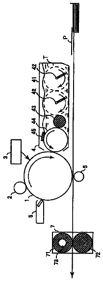
FIG. 3 is a schematic side view illustrating a structure of an image forming apparatus of the present invention; and
FIG. 4 is a drawing showing an X-ray diffraction spectrum of a crystal type oxotitaniumphthalocyanine of the present invention (Production Example 1).
It is an object of the present invention, therefore, to provide a photoreceptor that is free from generation of fine black dots and fogging under a high-temperature and high-humidity environment, that does not deteriorate in sensitivity under a low-temperature and low-humidity environment, that has high stability to environmental fluctuation, and that is applicable to a high-resolution machine, and an image forming apparatus including the photoreceptor.
The inventors of the present invention have made intensive studies to solve the above-described problems and, as a result, found that the above-described problems can be solved by including metal oxide microparticles that have gone through a specific surface treatment and a binder resin in an undercoat layer, and including a crystal type phthalocyanine having a specific X-ray diffraction pattern and an X-type metal-free phthalocyanine as a charge generation material in a photosensitive layer, to reach completion of the present invention.
The photoreceptor of the present invention comprises an undercoat layer between a conductive support and a photosensitive layer, wherein
the undercoat layer contains at least metal oxide microparticles coated with anhydrous silicon dioxide and a first binder resin,
the photosensitive layer is a monolayered photosensitive layer containing at least a charge generation material and a charge transport material or a multilayered photosensitive layer formed of a charge generation layer containing a charge generation material and a charge transport layer containing a charge transport material stacked in this order or in an inverse order, and
the charge generation material contains a crystal type oxotitanylphthalocyanine having peaks in an X-ray diffraction spectrum with CuK.alpha. characteristic X-rays (0.15418 nm) at Bragg angles (2.theta..+-.0.2.degree.) of 7.3.degree., 9.4.degree., 9.6.degree., 11.6.degree., 13.3.degree., 17.9.degree., 24.1.degree. and 27.2.degree., in which a peak bundle formed by overlapping the peaks at 9.4.degree. and 9.6.degree. is a largest peak, and the peak at 27.2.degree. is a second largest peak; and an X-type metal-free phthalocyanine having peaks in the X-ray diffraction spectrum at Bragg angles (2.theta..+-.0.2.degree.) of 7.5.degree., 9.1.degree., 16.7.degree., 17.3.degree. and 22.3.degree..
The present invention can provide a photoreceptor that is free from generation of fine black dots and fogging under a high-temperature and high-humidity environment, that does not deteriorate in sensitivity under a low-temperature and low-humidity environment, that has high stability to environmental fluctuation, and that is applicable to a high-resolution machine, and an image forming apparatus including the photoreceptor.
When the X-type metal-free phthalocyanine is contained in the photosensitive layer in a proportion of 10% by weight to 70% by weight with respect to the crystal type oxotitanylphthalocyanine, optimal sensitivity can be achieved and the above-described effects can be obtained more advantageously. When the photoreceptor is exposed with a semiconductor laser whose light intensity distribution is a Gaussian distribution, the photoreceptor is subjected to exposure/potential decay only by strong light in a central part but is not subjected to potential decay by weak light in an outer part, and therefore higher resolution can be attained.
When the metal oxide microparticles are coated with anhydrous silicon dioxide in a proportion of 0.1% by weight to 50% by weight, the above-described effects can be obtained more advantageously. In this case, in addition, influences of humidity fluctuation can be lessened while maintaining electrical characteristics of the metal oxide microparticles, in particular, titanium oxide microparticles.
When titanium oxide microparticles are used as the metal oxide microparticles and a polyamide resin is used as the first binder resin, the above-described effects can be obtained more advantageously. In this case, in addition, dispersibility improves in preparation of a coating solution for undercoat layer formation to inhibit generation of aggregates, allowing formation of a flat coating film. As a result, the resistance can be kept uniform to effectively inhibit generation of fine black dots. Furthermore, since the polyamide resin is easy to mix with the metal oxide microparticles and excellent in adhesion to the conductive support, flexibility of the film can be maintained.
When the metal oxide microparticles and the first binder resin are contained in the undercoat layer in a ratio by weight of 10:90 to 95:5, the metal oxide microparticles produce the above-described effects more advantageously.
When the film thickness of the undercoat layer is 0.05 .mu.m to 5 .mu.m, the above-described effects can be obtained more advantageously. In this case, in addition, sensitivity does not deteriorate under a low-temperature and low-humidity environment, and generation of fine black dots can be inhibited effectively at high temperature.
When the photosensitive layer is a multilayered photosensitive layer, the above-described effects can be obtained more advantageously. In this case, in addition, most suitable materials can be selected for each layer to produce the photoreceptor with no need to consider compatibility among the constituent materials.
The photoreceptor of the present invention will be described in detail with reference to the drawings, on the premise that the present invention is not limited to the following embodiments.
FIG. 1 is a schematic sectional view illustrating a structure of an essential part of a multilayered photoreceptor provided with a multilayered photosensitive layer (also referred to as "function separation type photosensitive layer") formed by stacking a charge generation layer and a charge transport layer in this order.
Specifically, in the photoreceptor of FIG. 1, an undercoat layer 7 and a photosensitive layer (multilayered photosensitive layer) 4 in which a charge generation layer 5 containing a charge generation material 2 and a charge transport layer 6 containing a charge transport material 3 are stacked in this order are formed in this order on a surface of a conductive support 1.
In the present invention, when the photosensitive layer is a multilayered photosensitive layer, the effects of the present invention can be obtained more advantageously, and most suitable materials can be selected for each layer to produce the photoreceptor with no need to consider compatibility among the constituent materials.
The multilayered photosensitive layer of FIG. 1 may be a reversely multilayered photosensitive layer in which the charge generation layer and the charge transport layer are stacked in an inverse order, but the embodiment of FIG. 1 is preferable.
FIG. 2 is a schematic sectional view illustrating a structure of an essential part of a monolayered photoreceptor provided with a monolayered photosensitive layer formed of a single layer.
Specifically, in the photoreceptor of FIG. 2, the undercoat layer 7 and a photosensitive layer (monolayered photosensitive layer) 4' containing the charge generation material 2 and the charge transport material 3 are formed in this order on the surface of the conductive support 1.
Hereinafter, each component of the present invention will be described in detail.
[Conductive Support 1]
The conductive support functions as an electrode of the photoreceptor and also as a support member for each layer.
The constituent material for the conductive support is not particularly limited as long as it is used in the relevant art.
Specific examples of the constituent material include metal and alloy materials such as aluminum, aluminum alloys, copper, brass, zinc, nickel, stainless steel, chromium, molybdenum, vanadium, indium, titanium, gold and platinum; and materials obtained by laying a metal foil, depositing a metal material or an alloy material, or depositing or applying a layer of a conductive compound such as a conductive polymer, tin oxide, indium oxide and carbon black on a surface of a substrate made of hard paper, glass or a polymer material such as polyethylene terephthalate, polyamide, polyester, polyoxymethylene, polystyrene, cellulose and polylactic acid.
The shape of the conductive support is not limited to a sheet form and a cylindrical form to be mentioned later in the layer structure illustrated in FIGS. 1 and 2, and may be a columnar form, an endless belt (seamless belt) form, or the like.
When each layer is formed on the conductive substrate by a dip coating method as in the case of an embodiment to be described later, the conductive support preferably has a cylindrical form.
As needed, the surface of the conductive support may be processed by anodic oxidation coating treatment, surface treatment using chemicals or hot water, coloring treatment or irregular reflection treatment such as surface roughing to the extent that the image quality is not adversely affected.
The irregular reflection treatment is particularly effective when the photoreceptor of the present invention is used in an electrophotographic process using a laser as an exposure light source. That is, since the wavelengths of laser light are uniform in the electrophotographic process using a laser as the exposure light source, the laser light reflected on the surface of the photoreceptor may interfere with the laser light reflected inside of the photoreceptor, resulting in appearance of interference fringes on an image and generation of an image defect. In this respect, the image defect that may be caused by the interference of laser light with uniform wavelengths can be prevented by giving the irregular reflection treatment to the surface of the conductive support.
[Undercoat Layer (Also Referred to as "Intermediate Layer") 7]
The undercoat layer has a function of preventing charges from being injected into the monolayered photosensitive layer or the multilayered photosensitive layer from the conductive support. In other words, deterioration in the chargeability of the monolayered photosensitive layer or the multilayered photosensitive layer is limited and therefore, a reduction in surface charges on a part other than the parts to be eliminated by the exposure to light is limited, thereby preventing the occurrence of image defects such as fogging. In particular, it is possible to prevent fogging of images called black dots, that is, fine black dots of toner formed on a white background in image formation by a reverse developing process.
The undercoat layer that coats the surface of the conductive support can reduce the degree of irregularities, which is a defect of the surface of the conductive support to uniform the surface, enhance the film-forming characteristic of the monolayered photosensitive layer or the multilayered photosensitive layer, and improve the sticking characteristics (adhesion) between the conductive support and the monolayered photosensitive layer or the multilayered photosensitive layer.
The undercoat layer of the present invention contains at least metal oxide microparticles coated with anhydrous silicon dioxide and a binder resin (first binder resin).
The "particles coated with a specific material", as used herein, means "particles surface-treated with a specific material".
Examples of the metal oxide microparticles include titanium oxide, zinc oxide, aluminum oxide, aluminum hydroxide and tin oxide microparticles. Out of these, in terms of conductivity and dispersibility, titanium oxide and zinc oxide microparticles are preferable, and titanium oxide microparticles are particularly preferable. That is, use of the titanium oxide microparticles as the metal oxide microparticles produces the effects of the present invention more advantageously and improves dispersibility in preparation of the coating solution for undercoat layer formation to inhibit generation of aggregates, allowing formation of a flat coating film. As a result, the resistance can be kept uniform to effectively inhibit generation of fine black dots.
Examples of the crystal type of the titanium oxide include an anatase type, a rutile type, amorphous and the like, and the crystal type of the titanium oxide microparticles of the present invention may be any of the above-mentioned types or may be a mixture of two or more of these types.
In addition, the shape of the metal oxide microparticles of the present invention may be dendritic, acicular or particulate, and is particularly preferably acicular, which allows achievement of a good balance between the film strength and the electrical characteristics.
The "acicular" shape, as used herein, may be a long and narrow form including a bar-like form, a columnar form and a spindle-like form; it does not need to be extremely long and narrow or sharp at an end.
The metal oxide microparticles preferably have an average primary particle diameter of 20 nm to 100 nm.
When the average primary particle diameter of the metal oxide microparticles is less than 20 nm, the dispersion efficiency of the metal oxide microparticles may decrease to cause aggregation, making generation of fine black dots in images more likely. It also leads to increase in liquid viscosity, which is not preferable in terms of storage stability. It is not preferable that the average primary particle diameter of the metal oxide microparticles is more than 100 nm, because in this case, chargeability in a micro area decreases in the formation of the undercoat layer, leading to generation of fine black dots.
Here, the average primary particle diameter of the metal oxide microparticles is determined by measuring and averaging 50 or more particles for the diameter based on an SEM (S-4100, product by Hitachi High-Technologies Corporation) photograph.
The powder volume resistance of the metal oxide microparticles is preferably 10.sup.5 .OMEGA.cm to 10.sup.10 .OMEGA.cm.
When the powder volume resistance is less than 10.sup.5 .OMEGA.cm, the resistance as that of the undercoat layer lowers, which may cause the undercoat layer to failure in functioning as a charge blocking layer. For example, the powder volume resistance of metal oxide particles that have undergone conductive treatment such as formation of a tin oxide conductive layer doped with antimony is as extremely low as 10.sup.0 .OMEGA.cm to 10.sup.1 .OMEGA.cm. An undercoat layer using such a conductive layer is unusable, because it does not function as a charge blocking layer and deteriorates in chargeability as a characteristic of the photoreceptor to generate defects such as image fogging and black dots.
On the other hand, when the powder volume resistance of the titanium oxide microparticles is more than 10.sup.10 .OMEGA.cm, that is, when the powder volume resistance of the titanium oxide microparticles is equal to or larger than the volume resistance of the binder resin, the resistance as that of the undercoat layer is so high that transfer of carriers generated when light is applied is inhibited, increasing the residual potential and reducing photosensitivity.
The surface of the metal oxide microparticles to be used in the present invention is coated (covered) with anhydrous silicon dioxide.
When surface-untreated titanium oxide microparticles are used, for example, aggregation of the titanium oxide microparticles due to long-term use or storage of the coating solution for undercoat layer formation is unavoidable even if the titanium oxide microparticles are sufficiently dispersed in the coating solution. That leads to defects in the coating film and uneven coating in the formation of the undercoat layer to make carrier injection from the conductive support more likely via aggregates as well as generate an image defects. As a result, fine black dots will be generated even in the presence of the undercoat layer.
When conventionally proposed titanium oxide microparticles are used, that is, titanium oxide microparticles surface-treated with alumina in order to improve dispersibility in the undercoat layer are used, it is necessary to produce a large amount of coating solution for, for example, forming the undercoat layer on the conductive support by a dip coating process. In this case, dispersion process over a long period of time may cause reaggregation of the titanium oxide microparticles to generate black dots, leading to reduction in image quality.
This is considered because the alumina on the surface of the microparticles peels off due to dispersion process over a long period of time to lessen the effect of the surface treatment and cause reaggregation of the titanium oxide microparticles to generate an image defect and make carrier injection from the conductive support more likely, leading to generation of fine black dots.
In addition, such black dots will be more significant with long-term use under a high-temperature and high-humidity environment, leading to significant reduction in image quality.
Furthermore, in the case of the use of titanium oxide microparticles surface-treated with an organic compound including silane coupling agents such as an alkoxysilane compound; sililating agents obtained by combining silicon with a halogen atom, a nitrogen atom, a sulfur atom or the like; and general coupling agents such as a titanate coupling agent and an aluminum coupling agent, the resistance of the undercoat layer increases to reduce sensitivity variation due to humidity fluctuation but reduce the sensitivity itself, leading to generation of image fogging. In addition, occurrence of such a phenomenon is significant with repeated use, in particular.
In addition, in the case of the use of titanium oxide microparticles surface-treated with a combination of alumina and silicon dioxide for sufficient surface treatment, the undercoat layer is likely to be affected by humidity under various environments, induced by water of crystallisation contained in the silicon dioxide. As a result, the sensitivity of the photoreceptor is affected as well as the image quality is reduced.
Unlike these surface-treated metal oxide microparticles, the metal oxide microparticles coated with anhydrous silicon dioxide allow provision of photoreceptors having excellent stability, being free from reduction in sensitivity under various environments and free from black dots and image fogging, because the silicon dioxide does not contain water of crystallization and influence by humidity is limited. In addition, the coating with the anhydrous silicon dioxide is less likely to peel off in the dispersion process over a long period of time to prevent aggregation of the titanium oxide, allowing stable production of the coating solution and formation of a uniform undercoat layer.
The metal oxide microparticles preferably have anhydrous silicon dioxide in a proportion of 0.1% by weight to 50% by weight, and more preferably have anhydrous silicon dioxide in a proportion of 1% by weight to 40% by weight.
When the proportion of the anhydrous silicon dioxide (amount of surface treatment) is in the above-mentioned range, the effects of the present invention can be obtained more advantageously and influence by humidity fluctuation can be inhibited while maintaining electrical characteristics of the metal oxide particles, in particular, titanium oxide microparticles.
When the proportion of the anhydrous silicon dioxide is less than 0.1% by weight, the surface of the titanium oxide microparticles cannot be coated sufficiently to prevent the effect of the surface treatment from being produced sufficiently. When the proportion of the anhydrous silicon dioxide is more than 50% by weight, on the other hand, the effect of the addition of the titanium oxide microparticles is lessened and the effect of the addition of the silicon dioxide microparticles is produced, which may cause reduction in sensitivity of the photoreceptor and generation of image fogging.
For the metal oxide microparticles coated with anhydrous silicon dioxide, commercially available products can be used. Examples thereof include:
zinc oxide microparticles surface-treated with anhydrous silicon dioxide such as
Maxlight ZS-032, product name, manufactured by Showa Denko K.K. (zinc oxide: 80% by weight, anhydrous silicon dioxide: 20% by weight); and
titanium oxide microparticles surface-treated with anhydrous silicon dioxide such as
Maxlight TS-04, product name, manufactured by Showa Denko K.K. (titanium oxide: 67% by weight, anhydrous silicon dioxide: 33% by weight) and
Maxlight TS-043, product name, manufactured by Showa Denko K.K. (titanium oxide: 90% by weight, anhydrous silicon dioxide: 10% by weight).
Preferably, the metal oxide microparticles are contained in the undercoat layer in a ratio by weight between the metal oxide microparticles and the binder resin of 10:90 to 99:1, and more preferably in a ratio by weight of 30:70 to 99:1, and even more preferably in a ratio by weight of 35:65 to 95:5.
When the ratio by weight of the metal oxide microparticles is in the above-mentioned range, the effects of the present invention can be obtained more advantageously.
When the ratio by weight between the metal oxide microparticles and the binder resin is less than 10:90, the sensitivity of the photoreceptor may be reduced, and charges may be accumulated in the undercoat layer to increase the residual potential. This phenomenon is particularly significant in repetition properties under a low-temperature and low-humidity environment. On the other hand, when the ratio by weight between the metal oxide microparticles and the binder resin is more than 95:5, aggregates are likely to be generated in the undercoat layer, and, an image defect of fine black dots is likely to be generated. In this case, at the same time, the content of the binder resin is lowered, and therefore adhesion to the conductive support is reduced and the undercoat layer will be likely to peel off.
Examples of usable materials for the binder resin include the same materials as in the case of the formation of a monolayered undercoat layer of a resin in the art.
The description continues in the full USPTO document.
About 5,821 words. The USPTO PDF has it with every drawing.
Fees are due 3.5, 7.5 and 11.5 years after grant. This patent expired on April 29, 2026, so the fee marked "not paid" was the one that went unpaid.
ELECTROPHOTOGRAPHIC PHOTORECEPTOR AND IMAGE FORMING APPARATUS INCLUDING THE SAME
Filed Jul 2010 · published Jan 2011Electrophotographic photoreceptor and image forming apparatus including the same
Filed Jul 2010 · granted Apr 2014Earlier publications, parents and continuations. None of them can still be enforced, or this patent would not be listed.
Prior art cited by the examiner or applicant. Useful when you check your own idea for novelty.
Everything on this page comes from the documents linked above.