Cross-reference to related application
This application is related to application Ser. Nos. 13/155,993, 13/155,922 and 13/155,945, commonly filed with the current application, with common title, inventor and commonly assigned.
Technical field
The present inventions relate to electronic sampling systems. More particularly, the inventions relate to circuits and methods that improve the performance of electronic sampling systems by reducing signal distortions commonly associated with the electronic implementation of such systems.
Background art
Sampling systems have a wide range of applications in electronics. For example, sampling systems are frequently found in popular consumer electronic devices such as MP3 players, DVD players and cellular telephones. Other popular uses of sampling systems include those related to data acquisition, test and measurement, and control system applications. More specifically, sampling systems and sample-based technology may be found in the electronic components used to construct such devices, which include analog-to-digital converters, switched capacitor networks, signal acquisition circuitry, comparators, and others.
In some applications, sampling systems employ sample and hold circuits that sample a voltage and maintain it in a storage device so that another circuit can measure or otherwise observe the acquired voltage. However, as is known in the art, the mere act of sampling a signal of interest causes a certain amount of distortion to be imparted to the sampled signal.
The signal distortion produced by components in the sampling circuitry tends to limit the useful voltage and frequency range of an input signal. Such distortion may be produced by various factors such as the non-linear resistance characteristics of switches in the sample and hold circuits, effects associated with turnoff thresholds, bulk effect, switch ratio match variations and process variations, etc. Distortion may also be produced by parasitic capacitances of switches in sampling circuits, signal dependent charge injection by switches in the sampling circuits, non-linear load currents flowing through input source resistances, etc.
A typical prior art sample and hold circuit 100 is shown in FIG. 1. Sample and hold circuit 100 generally includes a switch 110, such as a transistor or transmission gate, coupled between an input terminal 115 and a storage device such as sampling capacitor 120. The impedance of switch 110 can be controlled through a switch impedance control terminal 135, which allows switch 110 to function as an "open circuit" (i.e., have a relatively large impedance) when an "OFF" signal is applied to terminal 135, and alternatively, function as a "short circuit" (i.e., have a relatively low impedance) when an "ON" signal is applied to terminal 135.
When switch 110 is, for example, implemented as an N-channel MOS transistor, switch 110 is ON when voltage is applied to its control node, such as a gate, that is above its conductance threshold, and OFF when voltage is applied to its gate that is below its conductance threshold. As is known in the art, the degree to which switch 100 is turned ON or OFF is dependent on the magnitude of the signal applied at its control node. Thus, for example, switch 110 may be turned ON by applying a signal to its control node just above the conductance threshold, but may be turned on harder, improving conductivity characteristics, by applying a greater voltage. Conversely, switch 110 may be turned OFF if the control voltage drops below the conductivity threshold.
In operation, a time varying input signal is applied to input terminal 115. Control circuit 125 is coupled between command terminal 130 and control terminal 135. Control circuit 125 modulates switch impedance between high (OFF) and low (ON) in response to an external hold command signal applied at command node 130.
Sample and hold circuit 100 has two distinct states usually referred to as a sample state and a hold state. In the sample state, switch 110 is ON (i.e., presents a low impedance between input terminal 115 and sampling capacitor 120) thus forcing the signal on the sampling capacitor 120 to follow the input signal. In the hold state, switch 110 is "OFF" (i.e., presents a high impedance between input terminal 115 and sampling capacitor 120), thus the signal on capacitor 120 is maintained at its previous level and is substantially independent of the input signal.
As is known in the art, switch 110 can be implemented using various electronic and electro-mechanical components including, but not limited to, relays, armature switches, and transistors in various forms, including bipolar junction transistors (BJTs), field effect transistors (FETs), etc.
However, known sample and hold circuits, similar to those described above, suffer from various drawbacks and disadvantages. For example, because of certain properties associated with physical component implementations, switch impedance in the sample state is often not low enough for optimal signal transmission or may vary with the magnitude of the input signal. This may occur, at least in part, because the signal applied to the control node of switch 110 does not turn the transistor ON hard enough or its relation with respect to the device conduction threshold varies due to changes in the magnitude of the input signal.
The resulting undesired effect in the sample state is that the voltage signal stored on capacitor 120 will be different from the input signal applied at input terminal 115. Furthermore the difference between the voltage signal stored on capacitor 120 and the input signal may be a function of the instantaneous value of the input signal. Thus, the signal acquired during the hold state will be an imprecise representation of the input signal, and any subsequent signal processing blocks will be affected by these imprecisions. Such signal distortion becomes increasingly significant as the maximum frequency of the input signal increases and its magnitude becomes comparable with an available power supply range.
The performance of high speed sampling data systems such as analog-to-digital converters is sensitive to variations in time intervals between successive sample operations. This variation may be referred to as a sampling jitter. A component of the sampling jitter is the variation in the time delay from the moment the external hold command is asserted at command terminal 130 to the moment switch 110 enters its hold state (i.e., is OFF). Control circuit 125 typically requires a finite time interval to produce the control signal which will modulate the switch impedance from its sample value to its hold value. If the threshold at which this transition occurs is dependent upon the input signal, the result is sampling jitter. Accordingly, it is generally desirable to minimize the effect of the input signal upon the switch control signal transition threshold.
In an effort to overcome the drawback of sampling jitter, sampling switches are constructed using CMOS transmission gates. Using this implementation, however, with an input signal range comparable to the available power supply, the equivalent switch impedance variation during the sample state becomes significant and introduces increasing amount of distortion as the input signal frequency increases.
An early attempt to solve this problem is described in U.S. Pat. No. 5,170,075 to de Wit. As shown in FIG. 2, which is a general representation of the circuit proposed by de Wit, an input signal 215 is connected directly to a control circuit 225, and coupled to a sampling capacitor 220 through a switch 210. Said switch 210 is constructed using a MOSFET device. Control circuit 225 controls switch impedance via control terminal 235 in response to an external HOLD signal 230 and uses a set of boost capacitors (not shown) coupled to develop a pre-selected voltage, V.sub.P, which in the sample state, is superimposed upon the input voltage. The resulting compound voltage is used to control the switch impedance during the sample state. As a result, in the sample state, switch 210 is controlled using a fixed gate-to-channel voltage, which reduces the switch impedance variation with input signal. In addition, the transition threshold between the sample and hold states is determined by the magnitude of V.sub.P and is substantially independent of the input voltage.
Other attempts to overcome the disadvantages associated with known sampling circuits are presented in U.S. Pat. Nos. 5,500,612 and 6,118,326. The circuits described therein include significant circuitry coupled through additional switches to a sensitive input terminal. One undesirable consequence of these proposed configurations is an increase in signal dependent loading at the input as well as undesirable kick-back signals during the transition between the sample and the hold states. The additional signal dependent loading may translate into increased signal distortions due to the finite impedance of the external input signal driver.
Moreover, kick-back signals appear (due in part to various impedances present in real implementation) when the pre-selected V.sub.P voltage is superimposed upon the input signal. These signals present more difficult settling requirements for the external input signal driver thus increasing power consumption and cost. In addition, while the gate-to-channel voltage characteristics are somewhat improved, the channel-to-body potential still changes with the varying input signal. Consequently, the switch impedance during the sample state continues to vary due to the switch device body effect. Similarly, the transition threshold is also dependent upon the switch device body effect.
Another attempt to overcome the disadvantages associated with known sampling circuits is presented in U.S. Pat. No. 6,329,848 to Maes et al., which employs certain known isolation techniques to reduced loading at the input. More specifically, as shown in FIG. 3, which is a general representation of the circuit proposed by Maes et al., a dedicated buffer amplifier 345 is used to isolate a control circuit 325 from an input terminal 315. A switch 310 is implemented using a MOSFET device with its source and drain terminals coupled to the input terminal 315 and a sampling capacitor 320. A gate terminal 335 and a body terminal 340 are both driven by the control circuit 325.
The circuit of FIG. 3 separately controls gate-to-channel and channel-to-body voltages as a function of the input signal as reproduced by buffer 345 to reduce switch impedance variations during the sample state. In addition, the buffer amplifier 345 tends to reduce the undesirable loading of the input terminal. This approach, however, continues to suffer from various drawbacks. For example, despite some reduction in loading compared with other implementations, this implementation still adds some loading at the input terminal, imparting a certain amount of distortion on the input signal. Moreover, it requires the use of a dedicated buffer amplifier with good settling characteristics and negligible group delay, which is relatively expensive to produce.
Thus, in view of the foregoing, it would be desirable to provide circuitry and methods that improve the performance of electronic sampling systems by reducing signal distortions commonly associated with the physical implementations of such circuits.
Brief description of the drawings
The above and other objects and advantages of the present invention will be apparent upon consideration of the following detailed description, taken in conjunction with the accompanying drawings, in which like reference characters refer to like parts throughout, and in which:
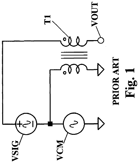
FIG. 1 is a schematic diagram of a prior art sample and hold circuit;
FIG. 2 is a schematic diagram of another prior art sample and hold circuit;
FIG. 3 is a schematic diagram of another prior art sample and hold circuit;
FIG. 4 is a generalized schematic diagram of one embodiment of a sample and hold circuit constructed in accordance with the principles of the present invention;
FIG. 5 is a schematic diagram of another embodiment of a sample and hold circuit constructed in accordance with the principles of the present invention; and
FIG. 6 is a more detailed schematic diagram of another embodiment of a sample and hold circuit constructed in accordance with the principles of the present invention.
FIG. 7 is a more detailed schematic diagram of another embodiment of a sample and hold circuit constructed in accordance with the principles of the present invention.
FIG. 8 is a more detailed schematic diagram of another embodiment of a sample and hold circuit constructed in accordance with the principles of the present invention.
FIG. 9 is a more detailed schematic diagram of another embodiment of a sample and hold circuit constructed in accordance with the principles of the present invention.
FIG. 10 is a more detailed schematic diagram of another embodiment of a sample and hold circuit constructed in accordance with the principles of the present invention.
FIG. 11 is a generalized schematic diagram of another embodiment of a sample and hold circuit constructed in accordance with the principles of the present invention; and
FIG. 12 is a more detailed schematic diagram of another embodiment of a sample and hold circuit constructed in accordance with the principles of the present invention.
Detailed description of the embodiments
A sampling circuit 400, constructed in accordance with the principles of the present invention, is shown in FIG. 4. As in FIG. 3, the sampling circuit of FIG. 4 generally includes a control circuit 425, a sampling switch 410, a capacitor or other suitable storage component 420, a command node 430, a switch control terminal 435, and an input terminal 415. In this example, the storage component 420 is a capacitor (although other suitable storage component may be used if desired).
One way in which sampling circuit 400 has been improved as compared to the sampling circuits shown in FIGS. 1-3, is by substantially reducing or eliminating all additional circuitry connected to the sensitive input terminal 415. In some embodiments, such remaining circuitry coupled to the input terminal may be disconnected during the sampling mode when its presence is most disadvantageous (discussed further below). As FIG. 4 shows, control circuit 425 is coupled between command node 430 and control terminal 435 of sampling switch 410.
FIG. 4 also shows that sampling switch 410 is coupled between input terminal 415 and capacitor 420. The impedance of switch 410 is controlled by control circuit 425, as determined by the external HOLD signal applied at the command node 430.
Similar to the prior art circuits illustrated in FIGS. 1-3, circuit 400 may operate in at least two different modes, sample mode and hold mode. In the sample mode, the impedance of sampling switch 410 is low, and thus the input signal at node 415 is typically applied to capacitor 420. In the sample mode, circuit 400 may operate as follows. An input signal may be applied to input terminal 415. A command signal, such as a HOLD signal, may then be applied (or toggled) at command node 430 causing the signal on control terminal 435 to turn sampling switch 410 ON.
Generally, a predefined charge, Q.sub.P is developed by control circuit 425, and is applied to sampling switch 410. This predefined charge develops a substantially constant gate-to-source control voltage for sampling switch 410, such that its impedance is maintained at a substantially constant level, which may be predetermined based on the turn ON characteristics of switch 410. For the purposes of illustration, assume Q.sub.P is selected such that the impedance of the transmission path in sampling switch 410 is and remains minimized with respect to the input signal (i.e., substantially constant). This arrangement allows the input signal at terminal 415 to charge capacitor 420 to its value without suffering from distortion associated with varying switch impedance.
In some embodiments, the HOLD command may be provided such that circuit 400 is maintained either in a sample or a hold state and merely toggles between the two. For example, the HOLD command may be either a logic high or logic low signal from an internal or an external source, placing the circuit 400 in one of the two modes. This may be done in order to prevent command node 430 from "floating" which may place circuit 400 in an indeterminate state.
Moreover, in some embodiments, predefined charge Q.sub.P may be selected in view of the turn ON characteristics of sampling switch 410 such that the circuit designer's desired switch impedance is substantially achieved and maintained, even with respect to a varying input signal. For example, a value of Q.sub.P may be selected in order to minimize switch impedance in view of the input signal while in sample mode and thereby minimize or eliminate any distortion on the acquired input signal.
In other embodiments, control circuit 425 may also include known circuitry (not shown) for adjusting Q.sub.P to account for manufacturing variations in switch characteristics or to account for changes due to component age, temperature variation, power supply variations, etc.
When sampling switch 410 is turned ON, the signal at input terminal 415 is applied to capacitor 420, which stores a value representative of the signal's magnitude. In traditional sample and hold circuits, capacitor 420 stores the magnitude of any input signal in the form of charge collected on the upper capacitor plate. The voltage stored thereon may be subsequently measured or otherwise observed and processed as desired.
In preferred embodiments, the duration of the sampling period is of sufficient time to allow for settling and ensure proper acquisition of the input signal. However, as will be understood from above, sampling switch 410 may remain ON as long as the HOLD signal directs it to do so. In such embodiments, the duration of the sampling period may be controlled by the HOLD signal. In other embodiments, a sample state may be maintained by a voltage stored on a certain capacitance associated with switch 410, which may remain until control terminal 435 is discharged when transitioning to a hold state.
As shown, the input terminal is preferably not connected to any circuitry responsible for toggling sampling switch 410 ON and OFF during the sampling mode. As a result, the input signal at node 415 does not experience any undesirable loading associated with circuitry in circuit 400 (other than that associated with capacitor 420 and switch 410), thereby reducing signal distortion. Moreover, the channel impedance of sampling switch 410 is maintained substantially constant by the predefined charge Q.sub.P allowing the input signal to pass substantially unaltered, further improving the quality of the sample obtained by capacitor 420.
After a sample has been obtained, circuit 400 may toggle from the sampling mode to the hold mode. One way this may be accomplished is by inverting the HOLD signal applied at command node 430. This may involve changing the HOLD signal from logic high to logic low or vice versa depending on the specific implementation of circuit components in circuit 400.
Choosing one convention for the purpose of illustration, assume that the HOLD signal changes from logic low (the sample mode) to logic high (the hold mode). When this occurs, switch 410 is turned OFF such that the input signal is disconnected from capacitor 420. When this occurs, control circuit 425 may discharge the gate of switch 410 and connect the gate to ground or other suitable OFF state control level. This turns switch 410 OFF, disconnecting it from the input signal at node 415, and thus isolating capacitor 420 from the input signal, placing circuit 400 in hold mode.
Referring now to FIG. 5, one possible implementation 500, constructed in accordance with the principles of the present invention, is shown. Circuit 500 is similar in certain respects to the circuit described in FIG. 4, and generally includes components and functional blocks which have been numbered similarly to denote similar functionality and general correspondence. For example, circuit 500 includes a storage capacitor 520 (capacitor 420 in FIG. 4), an input terminal 515 (input terminal 415 in FIG. 4), a sampling switch 510 (sampling switch 410 in FIG. 4), a control circuit 525 (control circuit 425 in FIG. 4) and a command node 530 (command node 430 in FIG. 4).
As shown, circuit 500 may include if necessary a charge pump 570 discussed below. The control circuit 525 may include a controlled current source 554, a switch 528 and a timing circuit 551. In this example, switch 528 may be a MOSFET transistor, a transmission gate or other suitable semiconductor device. Also as shown in this embodiment, timing circuit 551 may be a one-shot circuit, however, any other suitable timing circuit such as a latch, flip-flop, comparator, transient network, clock, or combination thereof may be used, if desired. The timing circuit 551 is triggered by a high-to-low signal transition at its control input.
Similar to circuit 400 of FIG. 4, circuit 500 may operate in at least two modes, a sample mode and a hold mode. Thus, circuit 500 may operate as follows. A logic high signal may be applied to command node 530. This signal turns switch 528 ON thus discharging the control node 535 and turning switch 510 OFF. This disconnects the input signal at node 515 from capacitor 520, isolating capacitor 520 and placing circuit 500 in a hold state.
To transition from a hold to a sample state, the HOLD signal at command node 530 is toggled from logic high to logic low. This turns switch 528 OFF, and causes the one-shot circuit 551 to generate a timing pulse (e.g., a relatively short duration logic high or logic low signal produced upon detecting a logic high-to-low transition at the trigger input) turning current source 554 ON for the duration T.sub.p. When ON, controlled current source 554 generates an output current I.sub.p.
Thus, a predefined charge Q.sub.p=I.sub.p*T.sub.p is applied to the gate of switch 510. This causes the voltage at the gate to rise, tending to turn switch 510 ON, which transitions circuit 500 from the hold state to the sample state.
As is known in the art, when the voltage at the gate of switch 510 rises above its turn ON threshold (with respect to channel potential) a gate to channel capacitance 511 (depicted as dotted lined capacitors) associated with the MOSFET switch 510 begins to develop. Generally speaking, while operating in this region, the gate of MOSFET switch 510 acts as a non-linear capacitor, with gate to channel capacitance 511 increasing as the voltage differential between the gate and channel becomes greater. Capacitance 512 (representing parasitic capacitance which may also be present at control node 535) absorbs some of the charge provided by current source 554, which undesirably causes the impedance of switch 510 to vary.
The amount of gate to channel capacitance 511 associated with MOSFET switch 510, however, can be determined, based on factors such as fabrication materials and process type, size and shape, etc., and thus taken into account (compensated for) in selecting the value of time interval T.sub.p or output current I.sub.p or both. Therefore, the amount of charge required by MOSFET switch 510 to fully turn ON can be calculated as the charge value Q.sub.p necessary to create a full turn ON voltage V.sub.ON between the gate and source of switch 510. In some embodiments, any parasitic capacitance 512 may also be included in the calculation to obtain a very high precision value for V.sub.ON. In specific implementations, the parasitic value may vary based on certain factors including circuit layout, material specifics, and any ancillary capacitive junctions.
By providing the appropriate amount of charge to control path 535 when turning MOSFET switch 510 ON, it is possible to substantially reduce or eliminate signal distortion associated with varying switch impedance encountered while circuit 500 is in the sample mode. This objective may be achieved by ensuring that the amount of charge delivered by current source 554 is substantially equal to the charge absorbed by gate to channel capacitance 511 (referred to as Q.sub.P) and parasitic capacitance 512 when a voltage V.sub.ON is developed between gate and source of MOSFET switch 510.
Accordingly, one way this may be accomplished is by determining the amount of instantaneous current produced by current source 554 (I.sub.p) and multiplying that value by the time period (T.sub.p) of the pulse generated by timing circuit 551 to obtain a total charge value (Q.sub.p). Once the charge value has been obtained, either the time period of the pulse (T.sub.p), or the value of current source 554 (or both) may be adjusted to ensure that Q.sub.p is applied to the gate of MOSFET switch 510 to obtain substantially constant switch impedance during sample state. This adjustment may be made at design time taking into account the expected properties of switch 510 and value of parasitic capacitance 512 or may be made at fabrication time (using well known trimming techniques) or may be made during circuit 500 operation (using well known tracking techniques such as replica and or ratio circuit monitors) or any combinations of the above. For example, the timing circuit 551 may adjust the duration T.sub.P of the timing pulse by monitoring the gate capacitance and parasitic capacitance of a device which substantially replicates the properties of switch 510 and/or control terminal 585.
Generally speaking, it is often desirable to have Q.sub.p applied to switch 511 as quickly as possible, to accelerate the acquisition of the input signal present at input node 515. This may be done, for example, to improve the sampling rate of circuit 500. Thus, in some embodiments, it may be desirable to configure current source 554 to provide an appropriate level of current such that substantially constant impedance is obtained relatively quickly (or as quickly as possible). For example, as in known in the art, the current generated by current source 554 may be selected by monitoring the gate capacitance and parasitic capacitance of a device which substantially replicates the properties of switch 510 and/or control terminal 535.
Once current source 554 turns OFF, the voltage imparted to control terminal 535 will remain substantially constant with respect to the input signal (until the HOLD signal toggles again, and the stored energy is dissipated through switch 528).
Furthermore, in certain circumstances, the associated voltage applied to the gate of transistor 510 during the sampling period may need to be greater than the rail voltage V.sub.DD in order to accommodate a wider range of input signals. One way this may be accomplished is by employing a charge pump or other voltage multiplier circuit known in the art to charge certain energy storage elements in circuit 500. For example, as shown in FIG. 5, charge pump 570 may be coupled to current source 554. In some embodiments, charge pump 570 (which may include one or more capacitors charged to suitable voltages and connected in successive series and parallel configurations to increase their overall voltage) may be coupled to command node 530. Thus, when a pulse from timing circuit 551 is received by current source 554, it may turn ON, establishing a current path through it (and/or charge pump 570) which conducts stored energy to the gate of switch 510, turning it ON. This arrangement allows switch 510 to be turned ON quickly and with enough energy to maintain the impedance of MOSFET switch 510 at the desired level (e.g., substantially constant) for a wide range of input signal levels.
Within this implementation, the size and capacity of energy storage devices in charge pump 570 may be calculated so they provide at least an appropriate Q.sub.P value to turn MOSFET switch 510 fully ON substantially instantaneously, such that switch impedance is and is maintained substantially constant, which, in some embodiments may be a minimum switch impedance, improving the accuracy of sampling circuit 500.
It will be understood that, depending upon the magnitude of the desired input signal range, the magnitude of the available power supply VDD, the characteristics of the semiconductor devices utilized, the desired sampling frequency and sampling settling time (and other similar factors), charge pump 570 may or may not be necessary in sampling circuit 500. Furthermore, when present, charge pump 570 may operate continuously, independent of the state (sample or hold) of sampling circuit 500 or operate on demand, as directed by HOLD command signal 530 (and as indicated by the dotted line connection of FIG. 5).
Referring now to FIG. 6, another possible specific implementation 600, constructed in accordance with the principles of the present invention, is shown. Like circuit 400, circuit 600 also is similar in certain respects to the circuit described in FIG. 4 and generally includes components and functional blocks which have been numbered similarly to denote similar functionality and general correspondence. For example, circuit 600 includes command node 630 (command node 430 in FIG. 4), control node 635 (control node 435 in FIG. 4), sampling switch 610 (sampling switch 410 in FIG. 4), control circuit 625 (control circuit 425 in FIG. 4) and capacitor 620 (capacitor 420 in FIG. 4), etc.
As shown, control circuit 625 may include charge transfer switch 631, discharge switch 628 and charge generator 650. Additional devices 629 and 632 limit the voltage across switches 628 and 631 respectively and may or may not be included, depending on the operating range of these devices (628 and 631). Charge generation circuit 650 may include transistors 656, 657, 658 and 659, inverter 652, and a timing circuit 651. In this example, the timing circuit 651 may be a one-shot circuit but other well known circuits such as flip-flops, logic gates, transistors and so on may be used if desired to implement the timing sequence described below. The timing circuit 651 is triggered by a high-to-low signal transition at its control input. A voltage level V.sub.CP present on rail 671 may be provided by another power source or (as shown in FIG. 6) by charge pump 670 functionally similar to charge pump 570 in FIG. 5.
As above, circuit 600 operates in at least two modes, a sample mode and a hold mode and may operate as follows. A logic high signal may be applied to the input of command node 630. This signal is preferably of sufficient magnitude to turn transistor 628 ON, which discharges control node 635 and the gate of switch 610, turning switch 610 OFF. This disconnects the input signal at node 615 from capacitor 620, isolating capacitor 620 and placing circuit 600 in a hold state.
The output of one shot circuit 651 in the hold mode is a logic low (close to ground), which causes the output of inverter 652 to be a logic high (close to VDD), driving the gate of switch 657 high (through capacitor connected transistor 659). This turns switch 657 ON, allowing capacitor connected transistor 656 to be charged close to the potential V.sub.CP of rail 671. The drain-to-gate voltage across device 631 is near zero maintaining switch 631 in the OFF state.
To transition from a hold to a sample state, the HOLD signal at command node 630 may be toggled from logic high to a logic low. This turns transistor 628 OFF, and causes timing circuit 651 to generate a short logic high pulse (e.g., a relatively short duration logic high signal produced upon detecting a logic high-to-low transition at the trigger input) which causes a short logic low pulse at the output of inverter 652. This allows capacitor connected transistor 656 to discharge through switch 631 and transistor 632, thus providing its stored charge to switch 610 via control terminal 635, turning switch 610 ON.
The amount of charge provided to switch 610 can be specified by a circuit designer by controlling the size ratio of capacitor connected transistor 656 and switch 610. For example, it may be desired to provide a calculated Q.sub.P value of charge to the gate of switch 610 which takes into account its gate to channel capacitance (shown as capacitors 611 in FIG. 6) and any parasitic capacitance encountered by charge traveling from capacitor 656 to the gate of switch 610 (represented by capacitor 612 in FIG. 6). When transferred to control terminal 635 the charge Q.sub.P generates an ON voltage V.sub.ON from the gate to the source of sampling switch 610 thus setting its sample mode impedance. Once the Q.sub.P value desired for switch 610 is calculated, the size of capacitor connected device 656 may be selected to provide it such that the impedance of switch 610 is minimized and maintained substantially constant. As an example, the physical implementation of device 656 may replicate or ratio the physical implementation of device 610, of its command node 635 and of its associated parasitic circuit elements.
It will be understood that although sampling circuit 600 may be used with a Q.sub.P value that minimizes the impedance of switch 610, that other values may be used to obtain any suitable substantially constant impedance desired (whether minimized or not). The timing pulse produced by circuit 651 should be selected such as to allow the transfer of the desired charge Q.sub.P to control terminal 635.
Because the magnitude or duration of the current pulse (thus the magnitude of the charge) provided by transistor connected capacitor 656 is not influenced by the voltage at the input terminal 615, the gate of sampling switch 610 will acquire a gate charge that is substantially independent from the voltage at input terminal 615, thus improving the precision of a sample obtained by capacitor 620.
Moreover, when the current pulse is OFF, at the end of the timing circuit 651 pulse, the voltage at the gate of sampling switch 610 with respect to the signal path will remain substantially fixed and independent of the input voltage. Thus, switch 610 is controlled without adding any additional circuitry connected to the sensitive input terminal 615 during sampling mode.
In some implementations of circuit 600, parasitic capacitance 612 associated with control terminal 635 may cause the ON impedance of MOSFET 610 to vary slightly as function of the input signal applied to input node 610. This variation typically occurs at the instant MOSFET 610 is turned ON. When the control terminal 635 settles as desired at a voltage V.sub.ON above the input voltage (applied at input terminal 615) the parasitic capacitance 612 must be charged to the same level directly dependent of the input voltage. Thus the parasitic capacitance 612 absorbs a fraction of the charge Q.sub.P which varies with the input voltage causing a variation in V.sub.ON final value. For example, if an input signal of two volts is initially applied to input node 615 (i.e., the source of MOSFET 610) prior to turning it ON, the charge at the gate of MOSFET 610 will be offset by the two volt source potential. This offset alters the turn ON level of MOSFET 610 (by the amount of charge absorbed by parasitic capacitor 612) and thus alters its impedance, which may undesirably impart distortion to any sampled signal. Because this offset will vary as a function of the input signal, the impedance of MOSFET 610 may also vary with respect to the input signal.
One way to address this problem is to provide a preset gate to source initialization voltage to MOSFET 610 (and implicitly to the parasitic capacitor 612) prior to providing the turn ON charge through switch 631. Such an initialization voltage may be derived from the input signal and applied to the gate of MOSFET 610 at the beginning of the sample mode but prior to signal acquisition (so it does not affect the input signal during acquisition). This allows the gate of MOSFET 610 to include an initialization voltage similar to (or the same as) that of the subsequently sampled signal to either fully or partially offset any gate to source voltage differential, and minimize instantaneous impedance variation, thereby improving the precision of the sampled signal.
One preferred embodiment of such a circuit is shown in FIG. 7 as circuit 700. Circuit 700 is similar in many respects to the circuit described in FIG. 6 and generally includes components and functional blocks which have been numbered similarly to denote similar functionality and general correspondence. For example, circuit 700 includes control circuit 725 (control circuit 625 in FIG. 6), charge generator circuit 750 (charge generator circuit 650 in FIG. 6) sampling switch 710 (sampling switch 610 in FIG. 6), and capacitor 720 (capacitor 620 in FIG. 6), charge pump circuit 770 (charge pump circuit 670 in FIG. 6) etc.
However, circuit 700 further includes gate initialization transistors 716 and 717, which are controlled by initialization control circuit 726 and an initialization charge generator circuit 780 (discussed in detail below).
As shown, control circuit 725 may include charge transfer switch 731, discharge switch 728 and charge generator 750. Additional devices 729 and 732 limit the voltage across switches 728 and 731 respectively and may or may not be included, depending on the operating range of these devices (728 and 731). Charge generation circuit 750 may include transistors 756, 757, 758 and 759, inverter 752 and a timing circuit 751. The timing circuit 751 is triggered by a low-to-high signal transition at its control input. Control circuit 725 and charge generator circuit 750 may operate the same as or similar to circuits 625 and 650 described above.
Circuit 700 further includes initialization control circuit 726 and initialization charge generation circuit 780. As shown, initialization control circuit 726 may include charge transfer switch 741, discharge switch 738 and charge generator 780. Additional devices 739 and 742 limit the voltage across switches 738 and 741 respectively and may or may not be included, depending on the operating range of these devices (738 and 741). Initialization charge generation circuit 780 may include transistors 787 and 788, capacitor coupled transistors 786 and 789, inverter 782, and a timing circuit 781. The timing circuit 781 is triggered by a high-to-low signal transition at its control input. Circuits 726 and 780 may operate the same as or similar to circuits 725 and 750 described above except that they generate signals at different times (e.g., circuits 725 and 750 provide an ON signal to MOSFET 710 during the sample mode when an input signal is being acquired by sampling capacitor 720 whereas circuits 726 and 780 provide an initialization signal to transistors 716 and 717 prior to acquiring the input signal to minimize or eliminate instantaneous impedance variation described above. In some embodiments, the initialization signal may be provided as an initial part of the sample mode as described below or, as an alternative, during the hold mode.
As above, circuit 700 operates in at least two modes, a sample mode and a hold mode and may operate as follows. A logic high signal may be applied to the input of command node 730. This signal is preferably of sufficient magnitude to turn transistor 728 ON, which discharges control node 735 and the gate of switch 710, turning switch 710 OFF. This disconnects the input signal at node 715 from capacitor 720, isolating capacitor 720 and placing circuit 700 in a hold state.
The description continues in the full USPTO document.
 Lapsed, fee not paid3 drawings