Technical field
The present invention relates to a method for producing a group III nitride semiconductor light-emitting device which is suitably used in light-emitting diodes (LEDs), laser diodes (LDs), or electronic devices; a group III nitride semiconductor light-emitting device; and a lamp.
Priority is claimed on Japanese Patent Application, No. 2008-147275, filed on Jun. 4, 2008, the contents of which are incorporated herein by reference.
Background art
Since a group III nitride semiconductor light-emitting device has a direct transition-type energy band gap which corresponds in range from the visible wavelength to the ultraviolet wavelength, and has excellent light-emitting efficiency, it has been used as a semiconductor light-emitting device, such as LEDs or LDs.
In addition, an electronic device having a group III nitride semiconductor has superior properties to those of conventional electronic devices having a group III-V compound semiconductor.
Such a group III-V compound semiconductor is generally produced by a metalorganic chemical vapor deposition (MOCVD) method using trimethyl gallium, trimethyl aluminum, and ammonia as a raw material. The MOCVD method is a method in which a carrier gas containing vapor of a raw material is supplied to the surface of a substrate, and the raw material is decomposed on the surface of the substrate heated to grow crystal of the raw material.
In the past, wafers made of a single crystal of Group III nitride semiconductor have not been marketed. In general, the Group III nitride semiconductor is obtained by growing a group III-V compound semiconductor crystal on a single crystal wafer containing a different compound from the semiconductor crystal. Therefore, there is a large lattice mismatch between the single crystal wafer containing a different compound from the semiconductor crystal and the group III-V compound semiconductor crystal obtained by epitaxial growth. For example, when gallium nitride (GaN) is grown on a sapphire (Al.sub.2O.sub.3) substrate, there is a 16% lattice mismatch between them. When gallium nitride is grown on a SiC substrate, there is a 6% lattice mismatch between them.
In general, when there is a large lattice mismatch, it is difficult to epitaxially grow crystal on a substrate directly. Even when crystal is epitaxially grown on the substrate, the density of the crystal is decreased, together with a decrease of crystallinity.
Then, when the Group III nitride semiconductor crystal is epitaxially grown on the sapphire substrate or a SiC single crystal substrate by the MOCVD method, in general, a layer, which is called a low-temperature buffer layer, and formed of aluminum nitride (AlN) or aluminum gallium nitride (AlGaN), is laminated, and then the group III nitride semiconductor crystal is epitaxially grown on the low temperature buffer layer (For example, Patent Documents Nos. 1 and 2).
In addition, a method in which a buffer layer is formed on the substrate by the sputtering method in advance, the substrate provided with the buffer layer is introduced into the MOCVD reaction furnace, and the group III nitride semiconductor layer is formed on the buffer layer, is also suggested (Patent Document No. 3). However, since the density and crystallinity of the crystal formed on the buffer layer are decreased, it is impossible to stably laminate an excellent crystal layer.
However, when the present inventors formed the buffer layer made of the above-mentioned material on the substrate by the sputtering method, and the gallium nitride-based compound semiconductor was laminated on the substrate provided with the buffer layer according to the Patent Documents Nos. 1 and 2, there was a limitation for improving the crystallinity of the gallium nitride-based compound semiconductor.
The reasons may be because the buffer layer contains amorphous phases or polycrystal phases in Patent Documents Nos. 1 and 2.
In the lamination methods using aluminum nitride, which is laminated by the sputtering as the buffer layer, disclosed in Patent Documents Nos. 3 and 3, due to the difference in lattice mismatch between the buffer layer and the gallium nitride layer, it is not possible to improve the crystallinity. [Patent Document No. 1] Japanese Patent (Granted) Publication No. 3026087 [Patent Document No. 2] Japanese Unexamined Patent Application, First Publication No. H4-297023 [Patent Document No. 3] Japanese Patent (Granted) Publication No. 3440873 [Patent Document No. 4] Japanese Patent (Granted) Publication No. 3700492
Disclosure of the invention
Problems to be Solved by the Invention
In consideration of the above-described problems, an object of the present invention is to provide a method for producing the group III nitride semiconductor light-emitting device which has excellent productivity and produce a group III nitride semiconductor light-emitting device having excellent light-emitting properties, in which a buffer layer is laminated on a substrate by a method capable of laminating a crystal layer having an excellent uniformity in a short time, and grows a group III nitride semiconductor having an excellent crystallinity on the buffer layer. In addition, another object of the present invention is to provide the group III nitride semiconductor light-emitting device, and a lamp comprising the group III nitride semiconductor light-emitting device.
Means for Solving the Problem
As a result of conducting diligent research to solve the problems, the present inventors found that the group III nitride semiconductor crystal can be obtained as an excellent, stable crystal by carrying out a pretreatment on a surface of the substrate in suitable conditions, exposing the surface of the substrate so as to match the crystal lattice structure between the surface of the substrate and the group III nitride compound, making a buffer layer on the substrate by activating with plasma and reacting at least metal gallium raw material and a gas containing a group V element. Thereby, the present inventors achieved the present invention.
That is, the present invention relates to the following inventions.
[1] A method for producing a group III nitride semiconductor light-emitting device, in which a buffer layer made of a group III nitride is laminated on a substrate, an n-type semiconductor layer comprising a base layer, a light-emitting layer, and a p-type semiconductor layer are laminated on the buffer layer in this order, comprising:
a pretreatment step in which the substrate is treated with plasma;
a buffer layer formation step in which the buffer layer having a composition represented by Al.sub.xGa.sub.1-xN (0.ltoreq.x<1) is formed on the pretreated substrate by activating with plasma and reacting at least a metal gallium raw material and a gas containing a group V element; and
a base layer formation step in which the base layer is formed on the buffer layer.
[2] A method for producing a group III nitride semiconductor light-emitting device according to [1], wherein the base layer is formed by a metalorganic chemical vapor deposition method in the base layer formation step.
[3] A method for producing a group III nitride semiconductor light-emitting device according to [1] or [2], wherein the pretreatment step is carried out by flowing a gas containing nitrogen into a chamber in a layer formation device.
[4] A method for producing a group III nitride semiconductor light-emitting device according to [3], wherein the partial pressure of the gas containing nitrogen which is flowed into the chamber is in a range of from 1.times.10.sup.-2 Pa to 10 Pa.
[5] A method for producing a group III nitride semiconductor light-emitting device according to any one of [1] to [4], wherein the pretreatment step is carried out in a chamber, and the pressure in the chamber is in a range of from 0.1 Pa to 5 Pa.
[6] A method for producing a group III nitride semiconductor light-emitting device according to any one of [1] to [5], wherein the time for the pretreatment step is in a range of from 30 seconds to 3,600 seconds.
[7] A method for producing a group III nitride semiconductor light-emitting device according to [6], wherein the time for the pretreatment is in a range of from 60 seconds to 600 seconds.
[8] A method for producing a group III nitride semiconductor light-emitting device according to any one of [1] to [7], wherein the temperature of the substrate in the pretreatment step is in a range of from 25.degree. C. to 1,000.degree. C.
[9] A method for producing a group III nitride semiconductor light-emitting device according to [8], wherein the temperature of the substrate in the pretreatment step is in a range of from 300.degree. C. to 800.degree. C.
[10] A method for producing a group III nitride semiconductor light-emitting device according to any one of [1] to [9], wherein the pretreatment step and the buffer layer formation step are carried out in the same chamber.
[11] A method for producing a group III nitride semiconductor light-emitting device according to any one of [1] to [10], wherein the plasma treatment in the pretreatment step is sputter cleaning.
[12] A method for producing a group III nitride semiconductor light-emitting device according to [11], wherein the sputter cleaning is carried out by generating plasma using an electrical power supply having high frequency in the pretreatment step.
[13] A method for producing a group III nitride semiconductor light-emitting device according to [12], wherein the sputter cleaning is carried out by generating nitrogen plasma using an electrical power supply having high frequency in the pretreatment step. [14] A method for producing a group III nitride semiconductor light-emitting device according to any one of [1] or [13], wherein the method further comprises a substrate processing step in which irregularity is formed on the surface of the substrate before the pretreatment step. [15] A method for producing a group III nitride semiconductor light-emitting device according to any one of [1] to [14], wherein the buffer layer is formed so as to cover at least 90% of a main surface of the substrate in the buffer layer formation step. [16] A method for producing a group III nitride semiconductor light-emitting device according to any one of [1] or [15], wherein the buffer layer is formed by a reactive sputtering method in the buffer layer formation step. [17] A method for producing a group III nitride semiconductor light-emitting device according to [16], wherein the buffer layer is formed by a reactive sputtering method which flows a gas containing the group V element into a reactor in the buffer layer formation step. [18] A method for producing a group III nitride semiconductor light-emitting device according to [16] or [17], wherein the buffer layer is formed by an RF sputtering method in the buffer layer formation step. [19] A method for producing a group III nitride semiconductor light-emitting device according to [18], wherein the buffer layer is formed by an RF sputtering method while moving a cathode magnet in the buffer layer formation step. [20] A method for producing a group III nitride semiconductor light-emitting device according to [16] or [17], wherein the buffer layer is formed by a DC sputtering method in the buffer layer formation step. [21] A method for producing a group III nitride semiconductor light-emitting device according to [20], wherein the buffer layer is formed by a pulse DC sputtering method in the buffer layer formation step. [22] A method for producing a group III nitride semiconductor light-emitting device according to any one of [1] to [21], wherein the group V element used in the buffer layer formation step is nitrogen. [23] A method for producing a group III nitride semiconductor light-emitting device according to any one of [1] to [22], wherein the gas containing the group V element used in the buffer layer formation step is ammonia. [24] A method for producing a group III nitride semiconductor light-emitting device according to any one of [1] to [23], wherein the temperature of the substrate in the buffer layer formation step is in a range of room temperature to 1,000.degree. C. [25] A method for producing a group III nitride semiconductor light-emitting device according to [24], wherein the temperature of the substrate in the buffer layer formation step is in a range of 200.degree. C. to 800.degree. C. [26] A method for producing a group III nitride semiconductor light-emitting device according to any one of [1] to [25], wherein the temperature of the substrate in the base layer formation step is 900.degree. C. or more. [27] A group III nitride semiconductor light-emitting device comprising a substrate; a buffer layer made of a group III nitride which is laminated on the substrate; an n-type semiconductor layer comprising a base layer which is laminated on the buffer layer; a light-emitting layer which is laminated on the n-type semiconductor layer; and a p-type semiconductor layer which is laminated on the light-emitting layer, wherein
the substrate is pretreated with plasma:
the buffer layer has a composition represented by Al.sub.xGa.sub.1-xN (0.ltoreq.x<1) which is obtained by activating with plasma and reacting at least a metal gallium raw material and a gas containing a group V element; and
the base layer is formed on the buffer layer.
[28] A group III nitride semiconductor light-emitting device according to [27], wherein the base layer is a layer which is formed by a metalorganic chemical vapor deposition method on the buffer layer.
[29] A group III nitride semiconductor light-emitting device according to [27] or [28], wherein the buffer layer is formed by a reactive sputtering method.
[30] A group III nitride semiconductor light-emitting device according to any one of [27] or [29], wherein the buffer layer is made of GaN.
[31] A group III nitride semiconductor light-emitting device according to any one of [27] to [30], wherein the substrate is made of sapphire.
[32] A group III nitride semiconductor light-emitting device according to any one of [27] to [31], wherein the buffer layer is formed so as to cover at least 90% of a main surface of the substrate.
[33] A group III nitride semiconductor light-emitting device according to any one of [27] to [32], wherein the buffer layer is made of a single crystal.
[34] A group III nitride semiconductor light-emitting device according to any one of [27] to [32], wherein the buffer layer contains columnar crystals.
[35] A group III nitride semiconductor light-emitting device according to any one of [27] to [34], wherein the thickness of the buffer layer is in a range of 10 to 500 nm.
[36] A group III nitride semiconductor light-emitting device according to any one of [27] to [35], wherein the thickness of the buffer layer is in a range of 20 to 100 nm.
[37] A group III nitride semiconductor light-emitting device according to any one of [27] to [36], wherein the base layer is made of a GaN-based compound semiconductor.
[38] A group III nitride semiconductor light-emitting device according to any one of [27] to [37], wherein the substrate has a main surface comprising a planar C plane and two or greater convex portions formed on the planar C plane, and the buffer layer covers the main surface of the substrate. [39] A group III nitride semiconductor light-emitting device according to [38], wherein the convex portion has a base width in a range of 0.05 to 5 .mu.m, a height in a range of 0.05 to 5 .mu.m, the height is 1/4 or greater relative to the base width, and an interval between adjacent convex portions is 0.5 to 5 times the base width. [40] A group III nitride semiconductor light-emitting device according to [38] to [39], wherein the convex portion has a shape of which an external form becomes smaller toward a top of the convex portion. [41] A group III nitride semiconductor light-emitting device according to any one of [38] to [40], wherein the convex portion has a substantially circular cone shape or a substantially polygonal pyramid shape. [42] A group III nitride semiconductor light-emitting device obtained by the method according to any one of [1] to [26]. [43] A lamp comprising the group III nitride semiconductor light-emitting device according to any one of [27] to [42].
Effects of the Present Invention
The method for producing a group III nitride semiconductor light-emitting device of present invention comprises the pretreatment step in which the substrate is treated with plasma; the buffer layer formation step in which the buffer layer having a composition represented by Al.sub.xGa.sub.1-xN (0.ltoreq.x<1) is formed on the pretreated substrate by activating with plasma and reacting at least a metal gallium raw material and a gas containing a group V element; and the base layer formation step in which the base layer is formed on the buffer layer. Therefore, the buffer layer having high uniformity and orientation can be formed.
In addition, since a base layer having high crystallinity can be formed on the buffer layer, lattice mismatch does not occur between the substrate and the semiconductor layer made of the group III nitride semiconductor. Due to this, it is possible to grow the group III nitride semiconductor having high crystallinity on the substrate with high efficiency. It is also possible to produce the group III nitride semiconductor light-emitting device having excellent light-emitting properties with high productivity.
In addition, the group III nitride semiconductor light-emitting device of the present invention comprises the substrate which is pretreated with plasma, the buffer layer which is formed on the pretreated substrate, and has a composition represented by Al.sub.xGa.sub.1-xN (0.ltoreq.x<1) which is formed by activating with plasma and reacting at least a metal gallium raw material and a gas containing a group V element, and the base layer which is formed on the buffer layer. Therefore, the layers constituting the group III nitride semiconductor, which are formed on the buffer layer, have excellent crystallinity. Due to this, it is possible to produce a group III nitride semiconductor light-emitting device having excellent light-emitting properties.
In addition, since the lamp of the present invention comprises the group III nitride compound semiconductor light-emitting device, the lamp has excellent light-emitting properties.
Brief description of the figures
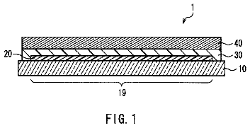
FIG. 1 is a view showing one example of the group III nitride semiconductor light-emitting device according to the present invention, and specifically a sectional view showing one example of the laminated semiconductor.
FIG. 2 is a planar view showing one example of the group III nitride semiconductor light-emitting device according to the present invention.
FIG. 3 is a sectional view showing one example of the group III nitride semiconductor light-emitting device according to the present invention.
FIG. 4A is a view showing one example of the group III nitride semiconductor light-emitting device according to the present invention, and specifically a sectional view showing a light-emitting device in which the buffer layer and the semiconductor layer are formed on the upper surface having convex portions of the substrate.
FIG. 4B is a view showing one example of the group III nitride semiconductor light-emitting device according to the present invention, and specifically a sectional view showing the lower position of the light-emitting device shown in FIG. 4A.
FIG. 4C is a view showing one example of the group III nitride semiconductor light-emitting device according to the present invention, and specifically a perspective view showing the shape of the substrate.
FIG. 5 is a sectional view showing the lamp provided with the group III nitride semiconductor light-emitting device according to the present invention.
FIG. 6A is a view showing one example of the group III nitride semiconductor light-emitting device according to the present invention, and specifically a sectional view showing a buffer layer laminated on the substrate.
FIG. 6B is a view showing one example of the group III nitride semiconductor light-emitting device according to the present invention, and specifically a sectional view showing another buffer layer laminated on the substrate.
FIG. 6C is a view showing one example of the group III nitride semiconductor light-emitting device according to the present invention, and specifically a sectional view showing another buffer layer laminated on the substrate.
FIG. 7 is a view explaining one example of the method for producing the group III nitride semiconductor light-emitting device according to the present invention, and specifically a view showing a sputtering device in which a target is provided in the chamber.
FIG. 8 is a graph explaining one example of the method for producing the group III nitride semiconductor light-emitting device according to the present invention, and specifically a graph showing the relationship between the temperature in the pretreatment step and an X-ray rocking curve in the
plane and the (10-10) plane of the base layer.
FIG. 9 is a graph explaining one example of the method for producing the group III nitride semiconductor light-emitting device according to the present invention, and specifically a graph showing the relationship between the time in the pretreatment step and an X-ray rocking curve in the
plane and the (10-10) plane of the base layer.
FIG. 10A is a graph explaining one example of the group III nitride semiconductor light-emitting device according to the present invention, and specifically a graph showing the relationship of a full width at half maximum of
plane X-ray rocking curve between the buffer layer and the base layer.
FIG. 10B is a graph explaining one example of the group III nitride semiconductor light-emitting device according to the present invention, and specifically a graph showing the relationship of a full width at half maximum of (10-10) plane X-ray rocking curve between the buffer layer and the base layer.
Best mode for carrying out the invention
Below, the method for producing a group III nitride semiconductor light-emitting device, the group III nitride semiconductor light-emitting device, and the lamp including the group III nitride semiconductor light-emitting device are explained referring to FIGS. 1 to 10.
Moreover, the size, thickness, etc. of each part illustrated in figures differ from real size, thickness, etc in the actual group III nitride semiconductor light-emitting device.
[Group III Nitride Semiconductor Light-Emitting Device]
For example, as shown in FIG. 3, in the group III nitride semiconductor light-emitting device (it may be called simply "light-emitting device") 1 of the present invention, a buffer layer 12 which is made of a group III nitride is formed on a substrate 11. The substrate 11 is treated with plasma in advance. An n-type semiconductor has a base layer 14a, a light-emitting layer 15, and a p-type semiconductor layer 16 laminated on the buffer layer 12 in this order. The buffer layer 12 is made of Al.sub.xGa.sub.1-xN (0.ltoreq.x<1) which is obtained by activating with plasma and reacting at least a metal gallium raw material and a gas containing a group V element. In addition, the base layer 14a is formed on the buffer layer 12 by the MOCVD method in this embodiment.
[Structure of the Light-Emitting Device]
FIG. 1 is a sectional view showing one example of the laminated semiconductor constituting the group III nitride semiconductor light-emitting device according to the present invention. Specifically, FIG. 1 is a sectional view showing one example of laminate semiconductor comprising the group III nitride semiconductor formed on the substrate 11.
In the laminate semiconductor 10 shown in FIG. 1, the buffer layer 12 having a composition represented by Al.sub.xGa.sub.1-xN (0.ltoreq.x<1) is formed on the substrate 11. The semiconductor layer 20 is formed on the buffer layer 12. The semiconductor layer 20 includes the n-type semiconductor layer having the base layer 14a which is formed on the buffer layer 12, the light-emitting layer 15, and the p-type semiconductor layer.
As shown in FIG. 2, which is a planar view, and FIG. 3, which is a sectional view, a transparent anode 17 is formed on the p-type semiconductor layer 16, and the anode bonding pad 18 is formed on the transparent anode 17 in the laminate semiconductor 10. In addition, a cathode 19 is laminated on an exposed area 14d formed on an n-type contact layer 14b of the n-type semiconductor layer 14. Thereby, the light-emitting device 1 of this embodiment is formed.
Below, a specific structure of the group III nitride semiconductor light-emitting device is explained.
[Substrate]
In general, materials on which the group III nitride semiconductor crystal can be epitaxially grown can be used as the material forming the substrate 11 on which the group III nitride semiconductor crystal is grown. Examples of the material for the substrate 11 include sapphire, SiC, silicon, zinc oxide, magnesium oxide, manganese oxide, zirconium oxide, manganese-zinc-iron oxide, magnesium-aluminum oxide, zirconium boride, gallium oxide, indium oxide, lithium-gallium oxide, lithium-aluminum oxide, neodium-gallium oxide, lanthanum-strontium-aluminum-tantalum oxide, strontium-titanium oxide, titanium oxide, hafnium, tungsten, molybdenum. Among these, materials having hexagonal crystal structure, such as sapphire and SiC, are preferable, because the group III nitride semiconductor having excellent crystallinity can be laminated. Furthermore, sapphire is the most preferable.
The size of the substrate is generally about two inches in diameter. However, the group III nitride semiconductor in the present invention can use the substrate having a diameter in a range of 4 inches to 6 inches.
When the buffer layer is formed without using ammonia, and the base layer is formed using ammonia, some oxide substrates and metal substrates cause chemical denaturation, because the substrates have contact with ammonia at high temperatures. Even when these oxide substrates and metal substrates are used, since the buffer layer acts as a coating layer, it is possible to prevent the chemical denaturation of the substrate in this embodiment of the present invention. In addition, in general, the sputtering can lower the temperature of the substrate. Due to this fact, even when the substrate is made of a material which decomposes at high temperatures, it is possible for each layer to be laminated on the substrate without causing any damage to the substrate 11.
[Buffer Layer]
In the laminate semiconductor 10 of this embodiment, the buffer layer 12 is formed on the substrate 11. The buffer layer 12 can be made of Al.sub.xGa.sub.1-xN (0.ltoreq.x<1) which is obtained by activating and reacting metal Ga raw material and a gas containing nitrogen elements by plasma. For example, the laminate semiconductor 10 can be formed by the reactive sputtering method. The layer which is obtained by the method using a plasma raw metal is easily orientated. Therefore, such a layer is preferably used as the buffer layer 12.
[Crystalline Structure]
The group III nitride crystal which makes the buffer layer formed using plasma raw metal has a hexagonal crystal structure. When the layer formation conditions are controlled, it is possible to make the group III nitride crystal be a single crystal. In addition, when the layer formation conditions are controlled, it is also possible to make the group III nitride crystal have a polycrystalline structure containing columnar crystals, that is, a texture based on hexagonal columnar crystals. Moreover, "columnar crystals" in the present invention means crystals each of which are separated by crystal grain boundaries between adjacent crystal grains, and has a columnar shape in longitudinal cross-section.
It is preferable that the buffer layer 12 have a single crystal structure, from the viewpoint of the functions of the buffer layer 12. As explained above, the group III nitride crystal is hexagonal, and forms a texture based on hexagonal columnar crystals. When the layer formation conditions are controlled, it is possible to make the group III nitride crystal grow in the in-plane direction. When the buffer layer having such a single crystal structure is formed on the substrate 11, the buffer layer effectively exerts the buffer functions. Thereby, the group III nitride semiconductor layer which is formed on the buffer layer 12 becomes a crystal layer having excellent orientation and crystallinity.
In addition, when the buffer layer has a polycrystal structure containing columnar crystals, it is preferable that an average grain width of the columnar crystals be in a range of 1 nm to 100 nm. The grain width of the crystals can be easily measured by cross-section observation of TEM (transmission electron microscope image).
[Composition]
The buffer layer 12 in the present invention is made of Al.sub.xGa.sub.1-xN (0.ltoreq.x<1) which is obtained by activating and reacting metal Ga raw material and a gas containing a group V element by plasma. Specifically, the buffer layer 12 can be made of GaN. In addition, it is possible to use a group III nitride, such as AlGaInN. Furthermore, it is also possible to add a group V element, such as As and P. When the buffer layer 12 contains Ga, the content of Ga is preferably 50% or more.
It is also possible to make the buffer layer 12 using a material having the same crystalline structure as that of the group III nitride semiconductor constituting the semiconductor layer 20. Among these materials, a material which has a similar lattice length to that of the group III nitride semiconductor constituting the following base layer 14a is preferably used. In particular, nitrides of the group IIIa elements are preferable.
[Thickness]
The thickness of the buffer layer 12 is preferably in a range of 10 nm to 500 nm. When the thickness of the buffer layer 12 is adjusted in the range, the buffer layer 12 having excellent orientation can be obtained. In addition, when the layers constituting the group III nitride semiconductor layer are formed on the buffer layer 12, the buffer layer 12 having the thickness in the range can act effectively as a coating layer.
When the thickness of the buffer layer 12 is less than 10 nm, the buffer layer 12 may not sufficiently act as the coating layer. In contrast, when it exceeds 500 nm, the time for producing the buffer layer is longer and the productivity is decreased, nevertheless there is no change of the functions as the buffer layer.
Moreover, the thickness of the buffer layer 12 is more preferably in a range of 20 nm to 100 nm.
[Covering Percentage]
When functions for covering the substrate 11 are concerned, it is preferable that the buffer layer 12 be formed so as to cover 60% or more, more preferably 80% or more, and most preferably 90% or more of the entire main surface 11a of the substrate 11. In particular, it is most preferable that the buffer layer 12 be formed so as to cover 100% of the main surface 11a of the substrate 11. In other words, it is most preferable that the buffer layer 12 be formed so as to cover the entire main surface 11a of the substrate 11 without exposing the main surface 11a. When the area of the main surface 11a of the substrate 11, which is covered with the buffer layer 12, is smaller, the substrate 11 is largely exposed. Due to this, the buffer layer 12 does not act as the coating layer. Thereby, since the semiconductor material for growing the group III nitride semiconductor crystal and the substrate react, there is a possibility that the flatness of the base layer 14a formed on the buffer layer 12 may decrease.
As shown in FIG. 6A, the buffer layer 12a may be formed on the substrate 11 so as to cover only the main surface 11a of the substrate 11 as shown in FIG. 6A. However, the buffer layer 12a may also be formed so as to cover the main surface 11a, and the side surfaces 11b of the substrate 11, as shown in FIG. 6B. As shown in FIG. 6C, it is most preferable that the buffer layer 12c be formed so as to cover the main surface 11a, the side surfaces 11b and the back surface 11c of the substrate 11, when the functions of the buffer layer as the coating layer are concerned.
As explained above, when the base layer 14a (the base layer 14a is explained below in detail) is formed by the MOCVD method, the raw gas may reach the side surfaces, and back surface of the substrate 11. In order to prevent the reaction between the raw gas and the substrate, it is most preferable that the buffer layer 12c be formed so as to protect the side surfaces and back surface of the substrate 11, as shown in FIG. 6C.
[Semiconductor Layer]
As shown in FIG. 1, the laminate semiconductor 10 in this embodiment includes the substrate 11, the buffer layer 12 formed on the substrate 11, and the semiconductor layer 20 formed on the buffer layer 12. The semiconductor layer 20 is made of the group III nitride semiconductor, and includes the n-type semiconductor 14 having the base layer 14a, the light-emitting layer 15, and the p-type semiconductor layer 16. In the laminate semiconductor 10 shown in FIG. 1, the base layer 14a provided with the n-type semiconductor layer 14 is formed on the buffer layer 12.
As the group III nitride semiconductor, for example, gallium nitride-based semiconductors, such as Al.sub.xGa.sub.YIn.sub.ZN.sub.1-AM.sub.A (0.ltoreq.X.ltoreq.1, 0.ltoreq.Y.ltoreq.1, 0.ltoreq.Z.ltoreq.1, X+Y+Z=1, M denotes group V element other than nitrogen (N), and 0.ltoreq.A<1) are well known. In the present invention, any gallium nitrides semiconductors represented by Al.sub.xGa.sub.YIn.sub.ZN.sub.1-AM.sub.A (0.ltoreq.X.ltoreq.1, 0.ltoreq.Y.ltoreq.1, 0.ltoreq.Z.ltoreq.1, X+Y+Z=1, M denotes a group V element other than nitrogen (N), and 0.ltoreq.A<1), and well-known gallium nitride-based semiconductors can be used without limitations.
The gallium nitride-based semiconductor can contain a group III element other than Al, Ga, and In. Specifically, the gallium nitride semiconductor can contain Ge, Si, Mg, Ca, Zn, Be, P, and/or As, if necessary. Furthermore, the gallium nitride semiconductor may contain not only the elements which are intentionally added but also impurities which are inevitably contained depending on the lamination conditions, or trace impurities which are contained in a raw material and reaction pipe, and the like.
[N-Type Semiconductor Layer]
In general, the n-type semiconductor layer 14 is laminated on the buffer layer 12, and includes the base layer 14a, the n-type contact layer 14b, and the n-type clad layer 14c. The n-type contact layer 14b can be served as the base layer 14a and/or the n-type clad layer 14c.
[Base Layer]
The base layer 14a in this embodiment is made of the group III nitride semiconductor, and is formed by laminating the group III nitride semiconductor on the buffer layer 12 by a well-known MOCVD method.
It is not always necessary that the base layer 14a be formed using the same material as that of the buffer layer 12 formed on the substrate 11. It is possible to form the base layer using the different material from that of the buffer layer 12. However, the base layer 14a is preferably made of Al.sub.yGa.sub.1-yN (0.ltoreq.y.ltoreq.1, preferably 0.ltoreq.y.ltoreq.0.5, and more preferably 0.ltoreq.y.ltoreq.0.1).
As the material for the base layer 14a, the group III nitride containing Ga, that is, a GaN-based compound semiconductor is preferable. In particular, AlGaN or GaN is preferably used.
The thickness of the base layer 14a is preferably in a range of 1 .mu.m to 10 .mu.m, because of obtaining excellent crystallinity. It is more preferably in a range of 5 .mu.m to 7 .mu.m, because of improving crystallinity and productivity, and reducing the time for forming the layer.
The base layer 14a may be doped with an n-type impurity in a range of from 1.times.10.sup.17 to 1.times.10.sup.19/cm.sup.3, if necessary. However, the base layer 14a may be undoped (<1.times.10.sup.17/cm.sup.3). The undoped base layer 14a is preferable, because it can maintain excellent crystallinity.
When a conductive substrate is used as the substrate 11, electrodes can be formed on both sides of the light-emitting device 1 by doping the base layer 14a.
When an insulating substrate is used as the substrate 11, electrodes, that is, the anode and the cathode, are formed on the identical surface of the light-emitting device 1. Therefore, the base layer 14a is preferably made of undoped crystals. When the base layer 14a is undoped, the base layer 14a has excellent crystallinity.
Moreover, any n-type impurities can be used. Examples of the n-type impurities include Si, Ge, and Sn. Si and Ge are preferable.
[N-Type Contact Layer]
The n-type contact layer 14b in this embodiment is made of the group III nitride semiconductor, and is formed on the base layer 14a by the MOCVD method or the sputtering method.
It is preferable that the n-type contact layer 14b be made of Al.sub.xGa.sub.1-xN (0.ltoreq.x.ltoreq.1, preferably 0.ltoreq.x.ltoreq.0.5, and more preferably 0.ltoreq.x.ltoreq.0.1), similar to the base layer 14a. In addition, the n-type contact layer 14b is preferably doped with the n-type impurities. The concentration of the n-type impurities is preferably in a range of from 1.times.10.sup.17 to 1.times.10.sup.19/cm.sup.3, and more preferably in a range of from 1.times.10.sup.18 to 1.times.10.sup.19/cm.sup.3. When the n-type impurities are doped in the range, it is possible to maintain excellent ohmic contact to the cathode and crystallinity, and prevent the generation of cracks. Any n-type impurities can be used. Examples of the n-type impurity include Si, Ge, and Sn. Among these, Si and Ge are preferable.
The growth temperatures of the n-type contact layer 14b is the same temperatures as those of the base layer 14a.
Moreover, as explained above, the n-type contact layer 14b may serve as the base layer 14a.
The gallium nitride-based semiconductor which constitutes the base layer 14a and the n-type contact layer 14b has preferably the identical composition.
The total thickness of the base layer 14a and the n-type contact layer 14b is preferably in a range of from 1 .mu.m to 20 .mu.m, more preferably in a range of from 5 to 15 .mu.m, and most preferably in a range of from 7 .mu.m to 12 .mu.m. When the total thickness of these layers is in the range, excellent crystallinity of the semiconductor can be maintained.
[N-Type Clad Layer]
It is preferable that the n-type clad layer 14c be formed between the n-type contact layer 14b and the light-emitting layer 15 (the light-emitting layer 15 is explained in detail below). When the n-type clad layer 14c is formed, it is possible to improve flatness of the outermost surface of the n-type contact layer 14b. The n-type clad layer 14c can be formed by the MOCVD method, etc using AlGaN, GaN, GaInN, etc. The n-type clad layer 14c also has the hetero junction structure of the layers made of AlGaN, GaN, or GaInN, or the superlattice structure in which the layer is laminated two or more times. When the n-type clad layer 14c is made of GaInN, it is needless to say that the band gap of the n-type clad layer 14c is preferably larger than that of the light-emitting layer 15.
The thickness of the n-type clad layer 14c is not limited, but it is preferably in a range of from 5 nm to 500 nm, and more preferably in a range of from 5 nm to 100 nm.
The concentration of the n-type dopant in the n-type clad layer 14c is preferably in a range of 1.times.10.sup.17 to 1.times.10.sup.20/cm.sup.3, and more preferably in a range of 1.times.10.sup.18 to 1.times.10.sup.19/cm.sup.3. When the concentration of the dopant is in the range, it is possible to maintain excellent crystallinity and decrease the operation voltage of the light-emitting device.
The description continues in the full USPTO document.
 Lapsed, fee not paid14 drawings