Background of the invention
Field of the Invention
The present invention relates to a method for forming a ferroelectric spontaneous polarization reversal in a desired region of a ferroelectric substrate, and more particularly to a method for forming a ferroelectric spontaneous polarization reversal that forms on a substrate having an electrooptic effect that is used for an optical element. In addition, it relates to a method for forming a ferroelectric spontaneous polarization reversal, where a ferroelectric substrate has convexo-concave structure on its surface and at a region including one portion of said convex part. Further, it relates to a method for forming a ferroelectric spontaneous polarization reversal capable of reversing the polarity of a narrow region of a substrate and also, capable of narrowing the interval between ferroelectric spontaneous polarization reversal regions.
Related Art Statement
An optical element such as a wavelength conversion element or an optical modulator is used in optical communication and optical measurement systems.
For example, a wavelength conversion element has periodical ferroelectric spontaneous polarization reversal structures on a substrate with an electrooptic effect such as a ferroelectric LiNbO.sub.3, as disclosed in the following patent document 1.
Also, as an example of an optical modulator, the optical modulator which has optical waveguides on a substrate with an electrooptic effect and has a ferroelectric spontaneous polarization reversal structure in one portion of the substrate related to said optical waveguides to suppress chirp generation or to improve extinction ratio of modulation intensity, as disclosed in the following patent document 2, has been proposed. [Patent Document 1] Japanese Patent Application Publication No. 2000-147584 [Patent Document 2] Japanese Patent Application Publication No. 2003-202530
As a method for forming a ferroelectric spontaneous polarization reversal region on a ferroelectric substrate, Ti thermal diffusion technique, heat treatment after loading SiO.sub.2 technique, and a proton exchange and following heat treatment technique can be cited. In addition, a method for forming a ferroelectric spontaneous polarization reversal region by applying an electric field higher than the value of coercive filed (e.g. 20 kV/mm for LiNbO.sub.3) is also known.
Specifically, ferroelectric spontaneous polarization reversal by applying an electric field is widely used as a method for forming a ferroelectric spontaneous polarization reversal because it is possible to form a ferroelectric spontaneous polarization reversal region accurately and the method for forming is simple.
As a method for forming a ferroelectric spontaneous polarization reversal by electric field, it has been proposed to apply a voltage 4 through electrodes 2 and 3 which are fabricated on the top and bottom faces of substrate 1 as shown FIG. 1, or to apply voltage 4 through electrodes 6 and 7 where conductive liquid is filled between substrate 1 and each electrode after fabricating insulating patterned mask 5 on the top face of substrate 1 using sealing members 8 and 9 at the same time as fixing said substrate as shown in FIG. 2. In addition, in case of using an insulating material such as an acrylic board instead of electrodes 6 and 7, it is arranged that an electric wire directly contact the conductive liquid for feeding of voltage 4.
By these methods, the ferroelectric spontaneous polarization reversal regions corresponding to the pattern of electrodes 2 and ferroelectric spontaneous polarization reversal regions corresponding to the region where the mask patterns 5 are not formed are formed respectively in FIG. 1 and FIG. 2.
For the methods for forming a ferroelectric spontaneous polarization reversal by electric field as stated above, when the width of a ferroelectric spontaneous polarization reversal region, for example a width L of a ferroelectric spontaneous polarization reversal region 10 formed on substrate 1 in FIG. 3 is less than 20 .mu.m, it is possible to form relatively homogeneous ferroelectric spontaneous polarization reversal regions because a homogeneous voltage is applied all over the region where a ferroelectric spontaneous polarization reversal is to be formed.
On the other hand, when a large ferroelectric spontaneous polarization reversal region having width L of more than 50 .mu.m is formed, it results in inhomogeneous ferroelectric spontaneous polarization reversal condition as a whole because a ferroelectric spontaneous polarization reversal is formed preferentially in the periphery of the region where a ferroelectric spontaneous polarization reversal is expected to be formed. Also, it becomes difficult to form a ferroelectric spontaneous polarization reversal homogeneously because of in-plane variation of wafer thickness and differences in voltage effects that are caused by dispersion of electric resistance of electrodes that apply an electric field. Thus, when a large diameter wafer is used, the differences of ferroelectric spontaneous polarization reversal condition depending on in-plane location of the wafer become prominent.
In the meantime, the following non patent documents 1 to 6 disclose that a process for forming a ferroelectric spontaneous polarization reversal comprises of the nucleation at the concentrated region of an electric field of an electrode edge, the expanding of microdomain in a depth direction so as not to increase electrostatic energy, the movement of domain wall in a transverse direction, and the stabilization of a ferroelectric spontaneous polarization reversal region, and these documents also disclose that the degree of nucleation density is important for homogeneity of a ferroelectric spontaneous polarization reversal.
In other words, it can be easily understood that, when a large region having width L of more than 50 .mu.m for forming a ferroelectric spontaneous polarization reversal, the polarity of the periphery is preferentially reversed, and that it is difficult to form a homogeneous ferroelectric spontaneous polarization reversal when width L is wide because the nucleation density is lower compared with when said width is narrow.
Thus, the non patent documents 1 to 6 propose a method for applying low electric field pulses into a substrate to generate nucleuses that are to be the nucleus of a ferroelectric spontaneous polarization reversal, and subsequently applying a high electric field pulse to extend domain wall from said nucleus to thereby realize a ferroelectric spontaneous polarization reversal.
Moreover, it has been reported that a homogeneous ferroelectric spontaneous polarization reversal region can be obtained by this method.
[Non Patent Document 1] Sunao KURIMURA et al., "Selective nucleation control for a periodically poled lithium niobate I .about.motivation and background.about.", Pre-Texts of the 49th Meeting; The Japan Society of Applied Physics and Related Societies, March 2002
[Non Patent Document 2] Takeshi AKUTSU et al., "Selective nucleation control for a periodically poled lithium niobate II .about.Periodical poling by selective nucleation control.about.", Pre-Texts of the 49th Meeting; The Japan Society of Applied Physics and Related Societies, March 2002
[Non Patent Document 3] Masayuki MARUYAMA et al., "Selective nucleation control for a periodically poled lithium niobate III .about.Qualification of nucleation density by particle analysis.about.", Pre-Texts of the 49th Meeting; The Japan Society of Applied Physics and Related Societies, March 2002
[Non Patent Document 4] Yoshiyuki NOMURA et al., "Selective nucleation control for a periodically poled lithium niobate IV .about.Pulse number dependence of nucleation density.about.", Pre-Texts of the 63rd Meeting; The Japan Society of Applied Physics, September 2002
[Non Patent Document 5] Masayuki MARUYAMA et al., "Selective nucleation control for a periodically poled lithium niobate V .about.Nucleation parameters for short period structure.about.", Pre-Texts of the 63rd Meeting; The Japan Society of Applied Physics, September 2002
[Non Patent Document 6] Masayuki MARUYAMA et al., "Selective nucleation control for a periodically poled lithium niobate VI .about.green light SHG with high-aspect-ratio periodicdomains.about.", Pre-Texts of the 50th Meeting; The Japan Society of Applied Physics and Related Societies, March 2003
Also, for an optical element such as an optical modulator, optical element having ridge structure has been put to practical use for the purposes of lowering drive voltage, matching impedance, and expanding bandwidth.
FIG. 7(a) is a perspective view of the optical element having ridge structure and FIG. 7(b) is a cross-sectional view of the substrate along the chain line A in FIG. 7(a). Modulating electrodes or the like are not shown in these figures.
An optical waveguide 112 is formed on a ferroelectric substrate 101 while a ridge 110 is formed on the region including said optical waveguide 112 in FIG. 7. Further, they show a ferroelectric spontaneous polarization reversal region 111 formed on one portion of an optical waveguide 112.
A method for forming a ferroelectric spontaneous polarization reversal in one portion of the ferroelectric substrate and subsequently removing a region where a ridge structure is not formed on the top face of said substrate selectively by mechanical cut or chemical etching as shown in FIG. 8 is a common method for forming a ferroelectric spontaneous polarization reversal in a region having convexo-concave structure such as a ridge structure on the top face of the ferroelectric substrate and including one portion of said convex part as shown in FIG. 7.
Regarding the specific procedures, at first, an electrode 120 having a desired pattern is formed on the top face of a ferroelectric substrate 101 and an electrode 121 is formed on all over the bottom face of said substrate as shown in FIG. 8(a). Then, a high voltage is applied between said electrodes 120 and 121 by a voltage source 122 to form a ferroelectric spontaneous polarization reversal 111 in the region corresponding to the pattern of electrode 120.
After that, electrodes 120 and 121 on the substrate are removed while a mask is formed corresponding to the pattern of a ridge structure formed on the top face of substrate 101. The substrate top face except the mask-covered region is removed chemically by dry etching or wet etching, or mechanically by sandblast or cutting to thereby form ridge structures 123 (see FIG. 8(b)). The concavity and convexity on the substrate surface where an optical waveguide is not formed as shown in the cross-sectional view of FIG. 7(b) are not shown in FIG. 8 to FIG. 14 to facilitate understanding of the description of the present invention.
However, it is difficult to form a desired ridge structure in the chemical removal process because the etching velocity and/or etching direction priority between the ferroelectric spontaneous polarization reversal region and the other region is different, and also, there is a disadvantage that in a mechanical removal process the substrate gets easy to break because the substrate receives much of a shock entirely.
Thus, it is required to form the ridge structure on a ferroelectric substrate firstly, and then, to form a ferroelectric spontaneous polarization reversal in a desired region of said substrate.
FIG. 9 show the method for forming a ferroelectric spontaneous polarization reversal after forming a ridge structure.
At first, optical waveguides 130 are formed on the top face of substrate 101 (see FIG. 9(a)), then, mask members 131 are formed on the region for forming a ridge structure on the top face of the substrate 101. After that, the region where mask members 131 are not formed is removed by etching or the like to thereby form ridge structures 132.
In order to form a ferroelectric spontaneous polarization in ferroelectric substrate 101 which has formed ridge structures 132, at first an electrode 133 is formed on the desired region of the top face of the substrate 101, and at the same time, an electrode 134 is formed all over the bottom face of the substrate 101. Then, a high voltage 135 is applied between both electrodes 133 and 134 to form a ferroelectric spontaneous polarization reversal 136 in the region of the substrate corresponding to the pattern of electrode 133 as shown in FIG. 9(d).
After forming a ferroelectric spontaneous polarization reversal, electrodes 133 and 134 are removed to obtain the substrate having the ridge structures where the polarity of one portion is reversed as shown in FIG. 9(e).
However, the ferroelectric spontaneous polarization reversal method in FIG. 9 has some negative effects such as the substrate becomes easy to break because the electric filed becomes concentrated at the edges 137 of electrode 133 formed on the ridge structure in FIG. 9(d), and further, when forming a ferroelectric spontaneous polarization reversal over the ridge structure and other regions, voltage adjustment in a ferroelectric spontaneous polarization reversal becomes complicated because the ridge and other regions are different in thickness and therefore, are different in strength of the electric field.
On the other hand, the method for using the insulating mask as shown in FIGS. 10 and 11 is cited as a method for forming a ferroelectric spontaneous polarization reversal in a ferroelectric substrate 101 which formed the ridge structure in FIG. 9(c).
In FIG. 10, an insulating mask 140 is formed on the top face of substrate 101 where a ferroelectric spontaneous polarization reversal is not formed. Said substrate is put between electrodes 142 and 143 with sealing members 141 while conductive liquids 145 and 146 are filled between a substrate 101 and each electrode 142 and 143, and a high voltage 144 is applied through the electrodes 142 and 143 like FIG. 2.
This method enables the forming of ferroelectric spontaneous polarization reversal 147 in the region of the substrate where the insulating mask 140 is not formed. The insulating mask is removed away after the ferroelectric spontaneous polarization reversal.
Also, in FIG. 11, an insulating mask 150 is formed on the bottom face of substrate 1 where a ferroelectric spontaneous polarization reversal is not formed. Said substrate is put between electrodes 152 and 153 with sealing members 151 while conductive liquids 155 and 156 are filled between a substrate 101 and each electrode 152 and 153, and a high voltage 154 is applied through the electrodes 152 and 153 like FIG. 2 or FIG. 10.
After that, a ferroelectric spontaneous polarization reversal 157 in the region of the substrate where the insulating mask 150 is not formed is formed, and subsequently the insulating mask 150 is removed.
However, the method, for forming a ferroelectric spontaneous polarization reversal using the insulating mask as shown in FIGS. 10 and 11 has a problem that the material for the insulating mask is limited because it is necessary to select the material having electric resistance higher than that of the ferroelectric substrate 101.
Furthermore, although when a resist mask that is widely used as the insulating mask is used here, hard baking treatment is effective in increasing the electric resistance value of a resist mask, it becomes difficult to remove the resist mask after forming a ferroelectric spontaneous polarization reversal. Moreover, the control accuracy of a ferroelectric spontaneous polarization reversal region declines because unintended micro ferroelectric spontaneous polarization reversal regions (micro-domain) are introduced into the substrate entirely due to the heat treatment, and operation troubles or a degradation of characteristics of a device using a ferroelectric spontaneous polarization reversal structure, such as a wavelength conversion element or an optical modulator, could be caused.
In addition, when an electric resistance value of an insulating mask cannot be raised adequately, a ferroelectric spontaneous polarization reversal region sometimes spreads to an unintended region of the substrate as shown by 148 of FIG. 10 or 158 of FIG. 11. It becomes difficult to control the formation of the ferroelectric spontaneous polarization reversal region accurately.
Further, the method for forming a ferroelectric spontaneous polarization reversal by the electrode pattern as shown in FIG. 1 or the insulating mask pattern as shown in FIG. 2 has problems that the fineness and the closeness of a ferroelectric spontaneous polarization reversal region are limited depending on the formation accuracy of a stroke width and/or a spacing of each pattern, and that the production process including to form a ferroelectric spontaneous polarization reversal becomes complicated because extra processes for forming patterns and removing the patterns have to be needed in the production process.
The first object of the present invention is to solve the problems described above and to provide a method for forming a ferroelectric spontaneous polarization reversal homogeneously even if the width of a ferroelectric spontaneous polarization reversal region is over 50 .mu.m, and further, to provide a method for forming a ferroelectric spontaneous polarization reversal that enable the lowering of the intensity of an applied voltage in a ferroelectric spontaneous polarization reversal.
The second object of the present invention is to provide a method for forming a ferroelectric spontaneous polarization reversal where the ferroelectric substrate has convexo-concave structure, such as ridge structure and the like, on its surface and the polarity of the region including one portion of said convex part is reversed with accuracy.
Moreover, the third object of the present invention is to provide a method for forming a ferroelectric spontaneous polarization reversal which could form a polarization reversal region closely, accurately and finely on a ferroelectric substrate, and also to provide the method for forming a ferroelectric spontaneous polarization reversal that is capable of preventing a production process from being complicated.
Summary of the invention
In order to solve the problems described above, a first aspect of the invention provides the method for forming a ferroelectric spontaneous polarization reversal in a desired region of a ferroelectric substrate, which has a feature that said desired region of a surface of said ferroelectric substrate is sprayed with micro-hard materials, made an impact by using a striking member that has micro tip diameter, or rubbed with micro-hard materials that are dispersively located on the surface of the substrate, and subsequently, a given voltage is applied into said desired region to thereby form a ferroelectric spontaneous polarization reversal in said desired region of said ferroelectric substrate.
A second aspect of the invention provides the method for forming a ferroelectric spontaneous polarization reversal in a desired region of a ferroelectric substrate, wherein, for said desired region of a surface of the ferroelectric substrate, an electrode pattern or a mask pattern is composed of aggregates of micropatterns, and subsequently a given voltage is applied into said desired region.
A third aspect of the invention provides the method for forming a ferroelectric spontaneous polarization reversal in a desired region of a ferroelectric substrate, where the thickness of substrate in said desired region of said ferroelectric substrate is thinner than the region except said desired region of the substrate, and a given voltage is applied into said desired region to thereby form a ferroelectric spontaneous polarization reversal in said desired region of said ferroelectric substrate.
A fourth aspect of the invention provides the method for forming a ferroelectric spontaneous polarization reversal according to the third aspect, which has a feature that a surface of the ferroelectric substrate is etched in order to make said ferroelectric substrate thinly.
A fifth aspect of the invention provides the method for forming a ferroelectric spontaneous polarization reversal according to any of the third and fourth aspects, which has a feature that the face for forming said ferroelectric substrate thinly is different from the face for forming a waveguide on said ferroelectric substrate.
A sixth aspect of the invention provides the method for forming a ferroelectric spontaneous polarization reversal, where a convexo-concave structure is formed on the top face of a ferroelectric substrate firstly, and then, a ferroelectric spontaneous polarization region is formed on the substrate including one portion of said convex part, which has a feature that a concave portion is formed on the bottom face of the substrate within the region where a ferroelectric spontaneous polarization reversal is to be formed and at least said convex portion is formed, and then, an electric field is applied into said substrate.
A seventh aspect of the invention provides the method for forming a ferroelectric spontaneous polarization reversal according to the sixth aspect, having a feature that the depth of said concave portion on the bottom face of the substrate is greater than the height of the convex portion on the top face of the substrate.
An eighth aspect of the invention provides the method for forming a ferroelectric spontaneous polarization reversal according to any of the sixth and seventh aspects, which has a feature that the width of said concave portion on the bottom face of the substrate is wider than the width of said convex portion on the top face of the substrate.
A ninth aspect of the invention provides the method for forming a ferroelectric spontaneous polarization reversal according to any of the sixth through eighth aspects, which has a feature that said electric field is applied via liquid electrode.
A tenth aspect of the invention provides the method for forming a ferroelectric spontaneous polarization reversal according to any of the sixth through ninth aspects, which has a feature that at least one portion of the region except said concave portion on the bottom face of the substrate is removed after forming a ferroelectric spontaneous polarization reversal.
An eleventh aspect of the invention provides the method for forming a ferroelectric spontaneous polarization reversal according to any of the sixth through ninth aspects, which has a feature that said concave portion on the bottom face of the substrate is filled entirely or partially with a material that has almost equal dielectric constant or coefficient of thermal expansion of said substrate after forming a ferroelectric spontaneous polarization reversal.
A twelfth aspect of the invention provides the method for forming a ferroelectric spontaneous polarization reversal where a concave portion is formed on the top face of a ferroelectric substrate or the bottom face of a ferroelectric substrate, an electric field is applied into the substrate, and a ferroelectric spontaneous polarization reversal is formed at least in one portion of a region of said substrate with said concave portion, which has a feature that the shape of said concave portion is configured such that the width of said concave portion gets narrower gradually toward the inside of the substrate.
A thirteenth aspect of the invention provides the method for forming a ferroelectric spontaneous polarization reversal according to the twelfth aspect, which has a feature that after first forming of a ferroelectric spontaneous polarization reversal, the top face of the substrate or the bottom face of the substrate that has already formed said concave portion is made almost a flat-plane, and then, a new concave portion is formed in a region where it was not formed previously, and after that an electric field is applied into said substrate to form a ferroelectric spontaneous polarization reversal again at least in one portion of the region of the substrate with said concave portion.
A fourteenth aspect of the invention provides the method for forming a ferroelectric spontaneous polarization reversal according to the twelfth aspect, which has a feature that the concave portions formed on the top and bottom faces of said substrate are placed in different geometric locations where the following ferroelectric spontaneous polarization reversal regions corresponding to said concave portions could not overlap.
A fifteenth aspect of the invention provides the method for a ferroelectric spontaneous forming polarization reversal according to any of the twelfth through fourteenth aspects, which has a feature that said applied electric field is gradually increased from a weak electric field including 0 to the given value of the electric field.
A sixteenth aspect of the invention provides the method for forming a ferroelectric spontaneous polarization reversal according to the twelfth through fifteenth aspects, which has a feature that said electric field is applied via liquid electrode.
In accordance with the first aspect of the invention, nucleuses are generated on the substrate surface by adding mechanical stress to the substrate surface using the methods for spraying the desired region of the ferroelectric substrate surface with the micro-hard materials, making an impact by the striking member that has micro tip diameter, or rubbing with the micro-hard materials that are dispersively located on the substrate surface, or the like.
Subsequently, centering on the nucleuses, a ferroelectric spontaneous polarization reversal is formed by applying the given voltage to said desired region.
This makes it possible to generate nucleuses within the region where it is desired to form a ferroelectric spontaneous polarization reversal as well as its periphery and to improve nuclear growth density. It is possible to achieve a homogeneous ferroelectric spontaneous polarization reversal even when a large dimension of a ferroelectric spontaneous polarization reversal region is formed.
Furthermore, for a LiNbO.sub.3 crystal or a LiTaO.sub.3 crystal, nucleuses on the substrate surface can be generated by a minute stress or impact, and therefore, a ferroelectric spontaneous polarization reversal region can be formed easily without using a large-scale equipment. Moreover, since it is very little nucleuses that are formed on the substrate surface and the mechanical load on the substrate is small as a whole, the mechanical property of the substrate itself does not deteriorate as a result.
In accordance with the second aspect of the invention, the use of micropatterns can generate nucleuses around each pattern, and, considering the whole polarization reversal region, it is possible to generate many nucleuses within the region. Even when a large dimension of a ferroelectric spontaneous polarization reversal region is formed, homogeneous polarization reversal can be realized.
In accordance with the third aspect of the invention, to make the thickness of the region of the substrate that is forming a ferroelectric spontaneous polarization reversal thinly enables to reduce applied voltage for forming a ferroelectric spontaneous polarization reversal. This method is effective to avoid troubles such as dielectric breakdown and this could also reduce the cost for mass production by degreasing requirements for the special fixture and/or power supply equipment.
In accordance with the fourth aspect of the invention, in the thinning process of said ferroelectric substrate thickness, there is no mechanical load on the substrate as a whole because etching is applied to the surface of said ferroelectric substrate and therefore the mechanical property of the substrate itself does not deteriorate as a result. Also, when a waveguide element is formed, it is desirable to remove the step that is formed after a ferroelectric spontaneous polarization reversal by polishing or the like because said step could cause an optical loss.
In accordance with the fifth aspect of the invention, it could provide an optical waveguide device that has no degradation of optical characteristics such as an optical loss because there is no affect of changing the substrate thickness because although one region of one face of the substrate corresponding to the shape of the ferroelectric spontaneous polarization reversal region is thinned by cut or etching, the optical waveguide is formed on the other face of the substrate. In this case, the process stated above of removing the step by polishing can be omitted.
In accordance with the sixth aspect of the invention, it becomes possible to increase the strength of an electric field in forming a ferroelectric spontaneous polarization reversal because a concave portion is formed on the bottom face of the ferroelectric substrate in a region where the convex portion is formed and the substrate in the region with the convex portion is thinned.
Thus, it becomes possible to form a polarization reversal accurately in said region of the substrate including said convex part.
In accordance with the seventh aspect of the invention, by making the depth of the concave portion formed on the bottom face of the substrate greater than the height of the convex portion formed on the top face of the substrate, the strength of an electric field applied to the region of the convex part on the substrate top face in forming polarization reversal can be equalized with or be made stronger than the strength of other regions where said concave portion is not formed on the bottom face of the substrate. Thus, it becomes possible to form polarization reversal accurately in said region of the substrate including said convex part.
In accordance with the eighth aspect of the invention, by making the width of the concave portion formed on the bottom face of the substrate wider than the width of the convex portion formed on the top face of the substrate, it becomes possible to form a ferroelectric spontaneous polarization reversal where said region of the substrate including the convex portion certainly. Moreover, it is possible to control a ferroelectric spontaneous polarization reversal region more clearly because the bottom edges of the convex portion and the bottom of the concave portion are located proximally, and as a result, a ferroelectric spontaneous polarization reversal is formed in the early stage of forming a ferroelectric spontaneous polarization reversal in this proximal section, and after that, a ferroelectric spontaneous polarization reversal makes progress in the region of the convex part.
In accordance with the ninth aspect of the invention, it is possible to apply an electric field all over the ferroelectric substrate corresponding to the thickness of the substrate, irrespective of convexo-concave structure on the top face or the shape of the convex portion on the bottom face of the substrate because a ferroelectric spontaneous polarization reversal is performed by the liquid electrode using conductive liquid. Thus, the ferroelectric spontaneous polarization reversal region can be controlled accurately by setting the shape of the top and bottom faces of the substrate with accuracy.
In accordance with the tenth aspect of the invention, by removing at least one portion of the region except said concave portion on the bottom face of the substrate after forming a ferroelectric spontaneous polarization reversal, it is possible to compensate a stress distribution over the ferroelectric substrate caused by a temperature change or a propagation characteristics change of a microwave or the like in case of using the ferroelectric substrate as an optical device.
In accordance with the eleventh aspect of the invention, by filling the whole or a portion of the concave portion on the bottom face of the substrate with the material having almost equal dielectric constant or coefficient of thermal expansion of said substrate after forming a ferroelectric spontaneous polarization reversal, it is possible to compensate the electrical characteristic of the substrate or the stress distribution related to the thermal expansion by adjusting the dielectric constant or a spatial distribution of coefficient of thermal expansion of the substrate.
In accordance with the twelfth aspect of the invention, since the shape of the concave portion is configured such that the width of said concave portion gets narrower gradually toward the inside of the substrate, the thickness of the substrate varies according to location within the concave portion. It is configured such that the thickness of the substrate gets thicker gradually from the deepest part of the concave portion toward the entry of the concave portion. Due to this configuration, it becomes possible to arbitrarily form a ferroelectric spontaneous polarization reversal region in accordance with the strength of an electric field applied into the substrate, centering on the deepest part of the concave portion and also within the width of the entry of the concave portion.
In other words, it becomes possible to form a ferroelectric spontaneous polarization reversal region with its width narrower than the entry shape of the concave portion.
In accordance with the thirteenth aspect of the invention, it could become possible to locate and form several ferroelectric spontaneous polarization reversal regions closely by using the method that firstly forming a ferroelectric spontaneous polarization reversal using the concave portion of the substrate, then, new concave portion is formed again on the region except said concave portion had formed previously.
In accordance with the fourteenth aspect of the invention, it could become possible to locate and form several ferroelectric spontaneous polarization reversal regions closely because the polarization reversal region formed by the concave portion on the top face of the substrate and the polarization reversal region formed by the concave portion on the bottom face of the substrate are located at different places within the substrate.
In accordance with the fifteenth aspect of the invention, it is possible to arbitrarily adjust a ferroelectric spontaneous polarization reversal region in accordance with the given strength of an electric field applied into the substrate, centering on the deepest part of the concave portion and also within the width of the entry of the concave portion, in such a manner that the electric field applied into the substrate is controlled to be gradually increased from the weak electric field including 0 to a given strength of an electric field in forming a ferroelectric spontaneous polarization reversal.
In accordance with the sixteenth aspect of the invention, it is possible to apply an electric field into the substrate effectively even when the concave portion is formed on the top face or bottom face of the substrate because the electric field is applied via the liquid electrode.
Brief description of the drawings
FIG. 1 is a diagram showing the method for forming a ferroelectric spontaneous polarization reversal using the electrode pattern according to the prior art;
FIG. 2 is a diagram showing the liquid electrode method according to the prior art;
FIG. 3 is a diagram showing the ferroelectric spontaneous polarization reversal region formed on the substrate;
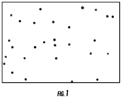
FIG. 4 is a diagram showing the micro-defects or the like formed on the surface of the substrate;
FIG. 5 are diagrams where a mask pattern is composed of aggregates of micropatterns;
FIG. 6 is a diagram showing a ferroelectric spontaneous polarization reversal being performed for the thinned substrate by the liquid electrode method;
FIG. 7 are diagrams showing the ferroelectric substrate having ridge structures; (a) is a perspective view of said substrate and (b) is a cross-sectional view of said substrate;
FIG. 8 are diagrams showing the example in which ridge structures are formed after a ferroelectric spontaneous polarization reversal according to the prior art;
FIG. 9 are diagrams showing examples in which polarization reversal is performed after forming ridge structures according to the prior art;
FIG. 10 is a diagram showing the example in which the insulating mask is formed on the surface of the ferroelectric substrate according to the prior art and a ferroelectric spontaneous polarization reversal is performed;
FIG. 11 is a diagram showing the example in which the insulating mask is formed on the bottom face of the ferroelectric substrate according to the prior art and a ferroelectric spontaneous polarization reversal is performed;
FIG. 12 is a diagram showing the concave portion being formed on the bottom face of the ferroelectric substrate of the present invention;
FIG. 13 is a diagram showing the method for forming a ferroelectric spontaneous polarization reversal for the ferroelectric substrate having the concave portion on the bottom face of the substrate according to the present invention;
FIG. 14 are diagrams showing the treatment after a ferroelectric spontaneous polarization reversal for the ferroelectric substrate having the concave portion on the bottom face of the substrate; (a) is a diagram in which the region except the concave portion is removed and (b) is a diagram in which the whole or a portion of said concave portion is filled in;
FIG. 15 are diagrams showing the example of the method for forming a ferroelectric spontaneous polarization reversal according to the present invention; (a) is a cross-sectional view of the structure of the substrate before a ferroelectric spontaneous polarization reversal and (b) is a diagram showing the condition after a ferroelectric spontaneous polarization reversal;
FIG. 16 are diagrams showing the method for forming a fine and close ferroelectric spontaneous polarization reversal regions by the method for forming a ferroelectric spontaneous polarization reversal according to the present invention; and
FIG. 17 are diagrams showing another method for forming a fine and close ferroelectric spontaneous polarization reversal region by the method for forming polarization reversal according to the present invention.
Explanations of numerals
1, 101, 201 Ferroelectric substrate 2 Patterned electrode 3 Bottom face electrode 4 Applied voltage 5 Insulating mask pattern 6, 7, 162, 163 Electrode 8, 9, 161 Sealing member 10, 167, 211, 221, 224, 232, 233 Ferroelectric spontaneous polarization reversal region 20 Micro-defects or micro-residual stress region 130 Optical waveguide 132 Ridge structure 160, 210, 220, 223, 230, 231 Concave portion 165, 166 Conductive liquid 167 Ferroelectric spontaneous polarization reversal region 170 Removed portion 71 Filled part
Detailed description of the invention
In the following, the preferred embodiments of the present invention are explained in detail.
FIG. 4 is a diagram showing many nucleuses generated on the surface of a ferroelectric substrate 1 for a ferroelectric spontaneous polarization reversal region 20.
If such nucleuses exist, a ferroelectric spontaneous polarization reversal is expanded around these nucleuses when an electric field is applied into the ferroelectric substrate. Thus, if these nucleuses exist moderately in a desired ferroelectric spontaneous polarization reversal region, it becomes possible to realize homogeneous ferroelectric spontaneous polarization reversal state across a large diameter ferroelectric wafer, even when a ferroelectric spontaneous polarization reversal is simultaneously performed for several large regions of over 25 .mu.m in a ferroelectric spontaneous polarization reversal region width within a large diameter ferroelectric wafer of over 2 inches in diameter.
The description continues in the full USPTO document.
 Lapsed, fee not paid3 drawings