Background of the invention
1. Field of the invention
The present invention relates to a light emitting device technology and, in particular, relates to a light emitter, a light emitting element, and a light emitting display device, which can provide a light emitting element structure that can ensure a long-term element light-emitting life duration with respect to a light emitting element of a film surface light-emitting type that can obtain a large aperture ratio, that can omit sealing of the light emitting element, and that can form a protective layer after transferring it to another film forming apparatus by breaking vacuum after formation of a transparent electrode.
2. Discussion of the Background
In general, as self-emitters of light for use in display devices, there are field emission elements and electroluminescence (EL) elements. Among them, the EL elements are divided into an organic EL element using an organic material as a light emitting layer, and an inorganic EL element using an inorganic material as a light emitting layer.
The organic EL element comprises an anode, a cathode, and an organic EL layer of a very thin film that is sandwiched between the electrodes of two kinds, i.e. the anode and the cathode, and made of an organic light-emitting compound. When a voltage is applied between the anode and the cathode, holes from the anode and electrons from the cathode are respectively injected into the organic EL layer and recombined, and molecules of the organic light-emitting compound forming the organic EL layer are excited due to energy produced thereupon. In the course of deactivation of the molecules thus excited toward the ground state, a luminous phenomenon is generated. The organic EL element is a light emitter utilizing this luminous phenomenon.
The organic EL layer has a single-layer structure or a multilayer stacked structure including at least one of an organic layer called a light emitting layer that emits light by recombination of holes and electrons, an organic layer called a hole transport layer that is liable to be injected with holes and reluctant to move electrons, and an organic layer called an electron transport layer that is liable to be injected with electrons and reluctant to move holes.
In recent years, the organic EL elements have been actively studied and being put to practical use. The organic EL element is an element having a basic structure wherein a thin film of a hole injection material such as triphenyldiamine (TPD) is formed by vapor deposition on a transparent electrode (hole injection electrode, i.e. anode) such as tin-doped indium oxide (ITO), and further, a fluorescent substance such as aluminum-quinolinol complex (Alq3) is stacked as a light emitting layer, and further, a metal electrode (electron injection electrode, i.e. cathode) such as AgMg having a small work function is formed. Inasmuch as a very high luminance, i.e. several 100 to several 10000 cd/m2, can be obtained at an applied voltage of about 10V, attention has been paid thereto for household electrical appliances, electrical equipment of automobiles, bicycles, airplanes, etc., displays, and so on. Such an organic EL element has a structure wherein, for example, an organic layer such as a light emitting layer is sandwiched between a scan (common line) electrode serving as an electron injection electrode, and a data (segment line) electrode serving as a hole injection electrode (transparent electrode), and formed on a transparent (glass) substrate. Those that are formed as displays are roughly divided into a matrix display that carries out dot display using scan electrodes and data electrodes arranged in a matrix, thereby to display information of an image, a character, or the like as an aggregate of those dots (pixels), and a segment display that displays those that independently exist as indicators having predetermined shapes and sizes. In case of the segment display, it is also possible to adopt a static driving system that displays the respective indicators separately and independently. On the other hand, in case of the matrix display, a dynamic driving is system is normally adopted wherein respective scan lines and data lines are driven in a time sharing manner.
Light emitters each forming a light emitting portion of an organic EL element are divided into a substrate surface light emitting type that uses a structure of a transparent substrate/a transparent electrode/a light emitting layer/a metal electrode wherein light generated in the light emitting layer is transmitted through the transparent electrode and the transparent substrate so as to be emitted, and a film surface light emitting type that uses a structure of a substrate/a metal electrode/a light emitting layer/a transparent electrode wherein light generated in the light emitting layer is transmitted through the transparent electrode so as to be emitted from the side of the film surface opposite to the side of the substrate surface.
The element of the substrate surface light emitting type is described in, for example, Applied Physical Letter, vol. 51, pp. 913-915
(Appl. Phys. Lett., 51, 913-915 (1987)).
The element of the film surface light emitting type is described in, for example, Applied Physical Letter, vol. 65, pp. 2636-2638
(Appl. Phys. Lett., 65, 2636-2638 (1994)).
However, in case of the foregoing substrate surface light emitting type, there has been raised a problem that since light is emitted from the side of the substrate surface, if an opaque substance such as a driving circuit or wiring is inserted between the substrate surface and the light emitting surface, light is blocked so that the aperture ratio and the luminance are lowered. Further, there has been a problem that since the metal electrode and the light emitting layer that are liable to be corroded are provided on the transparent electrode, unless sealing of the element is carried out without breaking vacuum after formation of the metal electrode, the light is emitting property is degraded. The sealing technique for the light emitter is described in, for example, Laid-open Unexamined Patent Publication No. H8-124677.
On the other hand, in case of the foregoing film surface light emitting type, even if a driving circuit, wiring or the like is inserted between the substrate surface and the light emitting surface, the aperture ratio is not lowered. Further, the metal electrode and the light emitting layer that are liable to be corroded are located between the transparent electrode and the substrate. Therefore, by selecting sizes and a positional relationship of patterns of the metal electrode, the light emitting layer and the transparent electrode, the light emitting property is not immediately degraded even if vacuum is broken after film formation of the transparent electrode, so that it becomes possible to omit sealing of the light emitting element, and to form a protective layer after transfer into another film forming apparatus by once breaking vacuum after the formation of the transparent electrode.
The present invention has been made in view of the foregoing problems and has an object to provide a light emitter, a light emitting element, and a light emitting display device, which can provide a light emitting element structure than can ensure a long-term element light-emitting life duration with respect to a light emitting element of a film surface light-emitting type that can obtain a large aperture ratio, that can omit sealing of the light emitting element, and that can form a protective layer after transferring it to another film forming apparatus by breaking vacuum after formation of a transparent electrode.
Summary of the invention
For example, the gist of a first invention of the present invention resides in a light emitter in which a pattern of a lower electrode is formed on a base, a pattern of a light emitting is layer is formed on the pattern of said lower electrode, and a transparent electrode is formed on the pattern of said light emitting layer, said light emitter characterized in that a pattern of said transparent electrode is larger than the pattern of said lower electrode.
Further, the gist of a second invention of the present invention resides in a light emitter in which a pattern of a lower electrode is formed on a base, a pattern of a light emitting layer is formed on the pattern of said lower electrode, and a transparent electrode is formed on the pattern of said light emitting layer, said light emitter characterized in that a pattern of said transparent electrode is formed over all the area of the pattern of said lower electrode.
Further, the gist of a third invention of the present invention resides in a light emitter in which a pattern of a lower electrode is formed on a base, a pattern of a light emitting layer is formed on the pattern of said lower electrode, and a transparent electrode is formed on the pattern of said light emitting layer, said light emitter characterized in that a pattern of said transparent electrode is larger than the pattern of said light emitting layer.
Further, the gist of a fourth invention of the present invention resides in a light emitter in which a pattern of a lower electrode is formed on a base, a pattern of a light emitting layer is formed on the pattern of said lower electrode, and a transparent electrode is formed on the pattern of said light emitting layer, said light emitter characterized in that a pattern of said transparent electrode is formed over all the area of the pattern of said light emitting layer.
Further, the gist of a fifth invention of the present invention resides in a light emitter according to any of the first to fourth inventions, characterized in that an element portion comprising said transparent electrode, said light emitting layer, and said lower electrode is an electroluminescence element.
Further, the gist of a sixth invention of the present invention resides in a light is emitter according to the fifth invention, characterized in that said electroluminescence element has a structure in which an organic thin film emits light due to applied current.
Further, the gist of a seventh invention of the present invention resides in a light emitter according to the fifth or sixth invention, characterized in that a hole injection layer is formed between said transparent electrode and said light emitting layer.
Further, the gist of an eighth invention of the present invention resides in a light emitter according to any of the fifth to seventh inventions, characterized in that an electron transport layer is formed between said transparent electrode and said light emitting layer.
Further, the gist of a ninth invention of the present invention resides in a light emitter according to the eighth invention, characterized in that a plurality of light emitters are independently formed in the state commonly using said electron transport layer.
Further, the gist of a tenth invention of the present invention resides in a light emitter according to the fifth or sixth invention, characterized by comprising a lower electrode layer formed on said base, an electron transport layer formed on said lower electrode layer, a light emitting layer formed on said electron transport layer and serving as a hole injection layer, and a metal electrode layer formed on said light emitting layer.
Further, the gist of an eleventh invention of the present invention resides in a light emitter according to the seventh or tenth invention, characterized in that a plurality of light emitters are independently formed in the state commonly using the hole injection layer.
Further, the gist of a twelfth invention of the present invention resides in a light emitter according to the fifth or sixth invention, characterized by comprising a transparent electrode layer formed on an end surface of a light guide member, a light emitting layer formed on said transparent electrode layer and serving also as a hole injection layer and an electron transport layer, and a metal electrode layer formed on said light emitting layer.
Further, the gist of a thirteenth invention of the present invention resides in a light emitter according to any of the first to twelfth inventions, characterized in that a plurality of light emitters are independently formed in the state commonly using said transparent electrode layer.
Further, the gist of a fourteenth invention of the present invention resides in a light emitter according to any of the first to thirteenth inventions, characterized by comprising at least three independent light emitters arrayed two-dimensionally, wherein a first light emitter or light emitter group emits light at wavelengths in a red region, a second light emitter or light emitter group emits light at wavelengths in a green region, and a third light emitter or light emitter group emits light at wavelengths in a blue region.
Further, the gist of a fifteenth invention of the present invention resides in a light emitter according to the fourteenth invention, characterized by having a structure that can simultaneously emit light at wavelengths in the red region, the green region and the blue region.
Further, the gist of a sixteenth invention of the present invention resides in a light emitter according to any of the first to thirteenth inventions, characterized in that a plurality of light emitters are arrayed independently and two-dimensionally, wherein each of them emits light in a mixed color of light in a blue region, light in a red region, and light in a green region.
Further, the gist of a seventeenth invention of the present invention resides in a light emitting element characterized by being constituted of an element portion having the light emitter according to any of the sixth to sixteenth inventions, and a current applying element electrically connected to said element portion for applying current to said element portion.
Further, the gist of an eighteenth invention of the present invention resides in a light emitting element according to the seventeenth invention, characterized in that said current applying element comprises a thin film transistor having a gate, a drain and a source, and one of said transparent electrode and said lower electrode is connected to one of said drain and said source.
Further, the gist of a nineteenth invention of the present invention resides in a light emitting element according to the seventeenth or eighteenth invention, characterized by including a switching element connected to said current applying element for selecting whether said current applying element flows current to said element portion comprising said transparent electrode, said light emitting layer and said lower electrode.
Further, the gist of a twentieth invention of the present invention resides in a light emitting element according to the nineteenth invention, characterized in that said switching element is configured to include at least one transistor, and a drain of the transistor included in said switching element is connected to a gate of a transistor included in said current applying element.
Further, the gist of a twenty-first invention of the present invention resides in a light emitting element according to the nineteenth or twentieth invention, characterized by including a switching element connected to said current applying element for selecting whether said current applying element flows current to said element portion comprising said transparent electrode, said light emitting layer and said lower electrode, and by including wiring for feeding current to said current applying element, and wiring for applying ON/OFF voltage information to said switching element.
Further, the gist of a twenty-second invention of the present invention resides in a light emitting display device characterized by including a plurality of light emitting elements each according to the twenty-first invention, wherein wiring for feeding current to said current applying element, and wiring for applying ON/OFF voltage information to said switching element and wiring for feeding current to said current applying element are arranged in a matrix.
Further, the gist of a twenty-third invention of the present invention resides in a light emitting display device according to the twenty-second invention, characterized in that an angle between wiring arranged in one direction and wiring arranged in another direction relative thereto is approximately perpendicular.
Brief description of the drawings
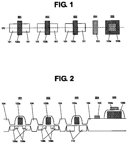
FIG. 1A is a sectional structure schematic view showing a light emitter according to one embodiment of the present invention;
FIG. 1B is a top perspective view thereof;
FIG. 2A is a sectional structure schematic view showing a light emitter according to one embodiment of the present invention;
FIG. 2B is a top perspective view thereof;
FIG. 3A is a sectional structure schematic view showing a light emitter according to one embodiment of the present invention;
FIG. 3B is a top perspective view thereof;
FIG. 4A is a sectional structure schematic view showing a light emitter according to one embodiment of the present invention;
FIG. 4B is a top perspective view thereof;
FIG. 5A is a sectional structure schematic view showing a light emitter according to one embodiment of the present invention;
FIG. 5B is a top perspective view thereof;
FIG. 6A is a sectional structure schematic view showing a light emitter according to one embodiment of the present invention;
FIG. 6B is a top perspective view thereof;
FIG. 7A is a sectional structure schematic view showing a light emitter according to one embodiment of the present invention;
FIG. 7B is a top perspective view thereof;
FIG. 8A is a sectional structure schematic view showing a light emitter according to one embodiment of the present invention;
FIG. 8B is a top perspective view thereof;
FIG. 9A is a sectional structure schematic view showing a light emitter according to one embodiment of the present invention;
FIG. 9B is a top perspective view thereof;
FIGS. 10A to 10D are diagrams showing one embodiment of stacked structures of light emitters that are applicable to the present invention;
FIGS. 11A to 11D are diagrams showing one embodiment of stacked structures of light emitters that are applicable to the present invention;
FIGS. 12A to 12D are diagrams showing one embodiment of stacked structures of light emitters that are applicable to the present invention;
FIGS. 13A to 13D are diagrams showing one embodiment of stacked structures of light emitters that are applicable to the present invention;
FIG. 14 is a conceptual view of a light emitting element according to one embodiment of the present invention;
FIG. 15 is a plan conceptual view showing an array of light emitting elements according to one embodiment of the present invention;
FIG. 16 is a plan schematic view showing a relationship between light emitters and wiring according to one embodiment of the present invention;
FIG. 17 is a plan schematic view showing a relationship between light emitters and wiring according to one embodiment of the present invention;
FIG. 18 is a plan schematic view showing a relationship between light emitters and wiring according to one embodiment of the present invention;
FIG. 19 is a plan schematic view showing an electrical connection relationship between a light emitting element and wiring according to one embodiment of the present invention;
FIG. 20 is a plan schematic view showing an electrical connection relationship between a light emitting element and wiring according to one embodiment of the present invention;
FIG. 21 is a plan schematic view showing an electrical connection relationship between a light emitting element and wiring according to one embodiment of the present invention;
FIG. 22 is a plan schematic view showing an electrical connection relationship between a light emitting element and wiring according to one embodiment of the present invention;
FIG. 23 is a plan schematic view showing an electrical connection relationship between a light emitting element and wiring according to one embodiment of the present invention;
FIG. 24 is a plan schematic view showing an electrical connection relationship between a light emitting element and wiring according to one embodiment of the present invention;
FIG. 25 is a sectional conceptual view showing an array of light emitting elements according to one embodiment of the present invention;
FIG. 26 is a sectional conceptual view showing an array of light emitting elements according to one embodiment of the present invention;
FIG. 27 is a sectional conceptual view showing an array of light emitting elements according to one embodiment `of the present invention;
FIG. 28 is a sectional conceptual view showing an array of light emitting elements according to one embodiment of the present invention;
FIG. 29 is a sectional conceptual view showing an array of light emitting elements according to one embodiment of the present invention;
FIG. 30 is a sectional conceptual view showing an array of light emitting elements according to one embodiment of the present invention;
FIG. 31 is a sectional conceptual view showing an array of light emitting elements according to one embodiment of the present invention;
FIG. 32 is a sectional conceptual view showing an array of a light emitting element according to one embodiment of the present invention;
FIG. 33 is a sectional schematic view showing a structure of a light emitting element according to one embodiment of the present invention;
FIG. 34 is a sectional schematic view showing a structure of a light emitting element according to one embodiment of the present invention;
FIG. 35 is a top schematic view showing a structure of a light emitting element according to one embodiment of the present invention;
FIG. 36 is a sectional schematic view showing a first fabrication process of a light emitting element according to one embodiment of the present invention;
FIG. 37 is a sectional schematic view showing a second fabrication process of a light emitting element according to one embodiment of the present invention;
FIG. 38 is a sectional schematic view showing a third fabrication process of a light emitting element according to one embodiment of the present invention;
FIG. 39 is a sectional schematic view showing a fourth fabrication process of a light emitting element according to one embodiment of the present invention;
FIG. 40 is a sectional schematic view showing a fifth fabrication process of a light emitting element according to one embodiment of the present invention;
FIG. 41 is a sectional schematic view showing a sixth fabrication process of a light emitting element according to one embodiment of the present invention;
FIG. 42 is a sectional schematic view showing a seventh fabrication process of a light emitting element according to one embodiment of the present invention;
FIG. 43 is a sectional schematic view showing an eighth fabrication process of a light emitting element according to one embodiment of the present invention;
FIG. 44 is a sectional schematic view showing a ninth fabrication process of a light emitting element according to one embodiment of the present invention;
FIG. 45 is a sectional schematic view showing a tenth fabrication process of a light emitting element according to one embodiment of the present invention;
FIG. 46 is a sectional schematic view showing an eleventh fabrication process of a light emitting element according to one embodiment of the present invention;
FIG. 47 is a sectional schematic view showing a twelfth fabrication process of a light emitting element according to one embodiment of the present invention; and
FIG. 48 is a top schematic view showing a structure of a light emitting element of a comparative example.
Detailed description of the illustrated embodiments
Embodiment 1
Herein below, an embodiment 1 of the present invention will be described in detail based on the drawings. FIG. 1A is a sectional schematic view showing a light emitter 14 of the present invention, and FIG. 1B is a top schematic view thereof. A base 1 is an object forming the light emitter 14, and includes a substrate or one comprising a substrate and a film or element formed thereon (hereinafter also applied). A pattern of a lower electrode 2a is formed on the base 1. On the lower electrode 2a is formed a pattern of a light emitting material layer 3a. The light emitting material layer 3a is a portion including at least a light emitting layer (e.g. later-described light emitting layer 7), which may also include an electron transport layer (later-described electron transport layer 6) or a hole injection layer (later-described hole injection layer 8) other than the light emitting layer (hereinafter also applied).
The pattern of the light emitting material layer 3a is larger than the pattern of the lower electrode 2a, and covers all the area of the pattern of the lower electrode 2a. That is, a pattern end portion 3b of the light emitting material layer 3a is located outside a pattern end portion 2b of the lower electrode 2a in all the area. A transparent electrode 4a is formed over the pattern of the light emitting material layer 3a. In FIG. 1A, the transparent electrode 4a is shown like it is not patterned. However, this means that a pattern thereof is so large that it can not be patterned in the range shown in the figure.
In the element structure of this embodiment, the transparent electrode 4a that is reluctant to corrode and is small in moisture permeability is formed over all the area of the lower electrode 2a and the light emitting material layer 3a. Therefore, even if the light emitter 14 having the element structure of this embodiment is exposed to the atmosphere by breaking vacuum, the lower electrode 2a and the light emitting material layer 3a can be shielded from moisture and oxygen contained in the atmosphere, so that the lower electrode 2a and the light emitting material layer 3a can be prevented from corrosion. Further, in this embodiment, a protective layer (later-described protective layer 16 shown in FIGS. 10 to 13) for strongly shielding the lower electrode 2a and the light emitting material layer 3a from water and oxygen in the atmosphere may also be formed on the transparent electrode 4a.
Embodiment 2
Herein below, an embodiment 2 of the present invention will be described in detail based on the drawings. The same symbols are assigned to those portions that are the same as those already described in the foregoing embodiment, thereby to omit overlapping description. FIG. 2A is a sectional schematic view showing a light emitter 14 of the present invention, and FIG. 2B is a top schematic view thereof. A pattern of a lower electrode 2a is formed on a base 1. On the lower electrode 2a is formed a pattern of a light emitting material layer 3a. The pattern of the light emitting material layer 3a is larger than the pattern of the lower electrode 2a, and covers all the area of the pattern of the lower electrode 2a. In FIG. 2A, the light emitting material layer 3a is shown like it is not patterned. However, this means that a pattern thereof is so large that it can not be patterned in the range shown in the figure. A pattern of a transparent electrode 4a is formed on the light emitting material layer 3a. The pattern of the transparent electrode 4a is is small than the pattern of the light emitting material layer 3a, but larger than the pattern of the lower electrode 2a. Further, all the area of the pattern of the lower electrode 2a is covered with the pattern of the transparent electrode 4a. That is, a pattern end portion 2b of the lower electrode 2a is located inside a pattern end portion 4b of the transparent electrode 4a in all the area.
In the element structure of this embodiment, the transparent electrode 4a that is reluctant to corrode and is small in moisture permeability is formed over all the area of the pattern of the lower electrode 2a and the light emitting material layer 3a. Here, the light emitting material layer 3a represents a portion of the light emitting material layer 3a, which is sandwiched between the pattern of the lower electrode 2a and the transparent electrode 4a and emits light by applying a voltage across the lower electrode 2a and the transparent electrode 4a. In this case, it approximately coincides with such a portion of the light emitting material layer 3a that is in contact with the lower electrode 2a.
Even if the light emitter 14 having the element structure of this embodiment is exposed to the atmosphere by breaking vacuum, the lower electrode 2a can be shielded from moisture and oxygen contained in the atmosphere, so that the lower electrode 2a can be prevented from corrosion.
Further, in the element structure of this embodiment, it is not necessary that the light emitting material layer 3a is precisely patterned to cover all the pattern of the lower electrode 2a and to be covered with the pattern of the transparent electrode 4a. Therefore, as compared with the structure shown in FIGS. 1A and 1B, fabrication is easy and reduction in fabrication cost can be achieved. However, of the light emitting material layer 3a, a portion not covered with the pattern of the transparent electrode 4a can not be shielded from oxygen and water. This area is away from the light emitting material layer 3a and has no direct relation to light emission. However, it is possible that corrosion of this area triggers exfoliation or the like of the light emitting material layer 3a to give influence on a light emission property. For using the element structure of this embodiment, it is desirable that a material reluctant to be corroded by water or oxygen is used for the light emitting layer.
In this embodiment, the case is shown wherein the pattern of the transparent electrode 4a is all formed on the pattern of the light emitting material layer 3a. However, such a case is also included wherein part of it is formed outside the pattern of the light emitting material layer 3a.
Further, in the element structure of this embodiment, a protective layer (later-described protective layer 16 shown in FIGS. 10 to 13) for strongly shielding the lower electrode 2a and the light emitting material layer 3a from water and oxygen in the atmosphere may also be formed on the transparent electrode 4a.
Embodiment 3
Herein below, an embodiment 3 of the present invention will be described in detail based on the drawings. The same symbols are assigned to those portions that are the same as those already described in the foregoing embodiments, thereby to omit overlapping description. FIG. 3A is a sectional schematic view showing a light emitter 14 of the present invention, and FIG. 3B is a top schematic view thereof. A pattern of a lower electrode 2a is formed on a base 1. On the lower electrode 2a is formed a pattern of a light emitting material layer 3a. Here, a case is shown wherein the pattern of the light emitting material layer 3a is all formed on the pattern of the lower electrode 2a. An insulating layer 5a is formed such that a pattern end portion 5b of the insulating layer 5a contacts with an end portion 3b of the light emitting material layer 3a. A pattern of a transparent electrode 4a is formed on the pattern of the light emitting material layer 3a so as to cover all of it.
In the element structure of this embodiment, the transparent electrode 4a or the insulating layer 5a is formed over all the area of the pattern of the lower electrode 2a. Further, the transparent electrode 4a is formed over all the area of the light emitting material layer 3a. Therefore, even if the light emitter 14 having the element structure of this embodiment is exposed to the atmosphere, the lower electrode 2a and the light emitting material layer 3a can be shielded from moisture and oxygen contained in the atmosphere by means of the transparent electrode 4a and the insulating layer 5a, so that the lower electrode 2a and the light emitting material layer 3a can be prevented from corrosion.
Further, the element structure of this embodiment is a structure wherein the patterns of the lower electrode 2a and the light emitting material layer 3a are buried using the insulating layer 5a, so that an upper surface of the element can be made relatively flat. Further, the pattern of the light emitting material layer 3a and the pattern of the lower electrode 2a can be firmly covered with the transparent electrode 4a and the insulating layer 5a, so that it is excellent in anticorrosion against oxygen and water. However, inasmuch as it is necessary to use the insulating layer 5a, one process is additionally required to increase the fabrication cost correspondingly.
Further, in the element structure of this embodiment, a protective layer (later-described protective layer 16 shown in FIGS. 10 to 13) for strongly shielding the lower electrode 2a and the light emitting material layer 3a from water and oxygen in the atmosphere may also be formed on the transparent electrode 4a.
Embodiment 4
Herein below, an embodiment 4 of the present invention will be described in detail based on the drawings. The same symbols are assigned to those portions that are the same as those already described in the foregoing embodiments, thereby to omit overlapping description. An element structure shown in FIGS. 4A and 4B is a modification of the element structure shown in FIGS. 3A and 3B, wherein a pattern end portion 5b of an insulating layer 5a rides on a pattern of a light emitting material layer 3a. By providing an overlapping portion of the insulating layer 5a and the light emitting material layer 3a, it is possible to reduce occurrence of leakage current between a pattern of a lower electrode 2a and a pattern of a transparent electrode 4a, which is caused by a fabrication error. On the other hand, because of the existence of the overlapping portion of the insulating layer 5a and the light emitting material layer 3a, flatness of an upper surface of the element is degraded as compared with the case of the foregoing embodiment 3 (FIG. 3).
Further, in the element structure of this embodiment, a protective layer (later-described protective layer 16 shown in FIGS. 10 to 13) for strongly shielding the lower electrode 2a and the light emitting material layer 3a from water and oxygen in the atmosphere may also be formed on the transparent electrode 4a.
Embodiment 5
Herein below, an embodiment 5 of the present invention will be described in detail based on the drawings. The same symbols are assigned to those portions that are the same as those already described in the foregoing embodiments, thereby to omit overlapping description. FIG. 5A is a sectional schematic view showing a light emitter 14 of this embodiment, and FIG. 5B is a top schematic view thereof. A pattern of a lower electrode 2a is formed on a base 1. On the lower electrode 2a is formed a light emitting material layer 3a.
A pattern of the light emitting material layer 3a covers all the area of the pattern of the lower electrode 2a. A pattern of a transparent electrode 4a is formed thereon so as to cover all the pattern of the lower electrode 2a. An insulating layer 5a is formed on the light emitting material layer 3a such that a pattern end portion 5b of the insulating layer 5a contacts with a pattern end portion 4b of the transparent electrode 4a. Although not shown in this embodiment, the insulating layer 5a is formed so as to cover all the portion of the light emitting material layer 3a, which is not covered with the transparent electrode 4a. In the element structure of this embodiment, the transparent electrode 4a is formed over all the area of the pattern of the lower electrode 2a. Further, the transparent electrode 4a is formed over all the area of the light emitting material layer 3a. Therefore, even if the light emitter 14 having the element structure of this embodiment is exposed to the atmosphere, the lower electrode 2a and the light emitting material layer 3a can be shielded from moisture and oxygen contained in the atmosphere by means of the transparent electrode 4a and the insulating layer 5a, so that the lower electrode 2a and the light emitting material layer 3a can be prevented from corrosion.
Further, the element structure of this embodiment is a structure wherein the pattern of the transparent electrode 4a is buried using the insulating layer 5a, so that an upper surface of the element can be made relatively flat. Further, the pattern of the light emitting material layer 3a and the pattern of the lower electrode 2a are all covered with the transparent electrode 4a and the insulating layer 5a, so that it is excellent in anticorrosion against oxygen and water. However, inasmuch as it is necessary to use the insulating layer 5a, one process is additionally required to increase the fabrication cost correspondingly. Further, in the element structure of this embodiment, a protective layer (later-described protective layer 16 shown in FIGS. 10 to 13) for strongly shielding the lower electrode 2a and the light emitting material layer 3a from water and oxygen in the atmosphere may also be formed on the transparent electrode 4a.
Embodiment 6
Herein below, an embodiment 6 of the present invention will be described in detail based on the drawings. The same symbols are assigned to those portions that are the same as those already described in the foregoing embodiments, thereby to omit overlapping description. An element structure shown in FIGS. 6A and 6B is a modification of the element structure shown in FIGS. 5A and 5B, wherein a pattern end portion 5b of an insulating layer 5a is formed in an overlapping manner so as to be located over a pattern end portion 4b of a transparent electrode 4a. By providing an overlapping portion of the insulating layer 5a and the transparent electrode 4a, it is possible to prevent generation of a gap between the pattern end portion 5b of the insulating layer 5a and the pattern end portion 4b of the transparent electrode 4a caused by a fabrication error, thereby to lower probability of corrosion of a light emitting material layer 3a. However, because of existence of an overlapping portion of the insulating layer 5a and a light emitting material pattern (a pattern of light emitting material layer 3a), flatness of an upper surface of the element is degraded as compared with the case of the foregoing embodiment 5 (FIG. 5).
Further, in the element structure of this embodiment, a protective layer (later-described protective layer 16 shown in FIGS. 10 to 13) for strongly shielding the lower electrode 2a and the light emitting material layer 3a from water and oxygen in the atmosphere may also be formed on the transparent electrode 4a.
Embodiment 7
Herein below, an embodiment 7 of the present invention will be described in detail based on the drawings. The same symbols are assigned to those portions that are the same as those already described in the foregoing embodiments, thereby to omit overlapping description. FIGS. 7A and 7B are a sectional view and a plan view of a light emitting element 65 wherein a plurality of light emitters 14 are arrayed. In each of the light emitters 14, a pattern of a lower electrode 2a is formed on a base 1 and, on the pattern of the lower electrode 2a, a pattern of a light emitting material layer 3a is formed so as to cover all the area thereof. On the pattern of the light emitting material layer 3a is formed a pattern of a transparent electrode 4a so as to cover all the area thereof. Here, a pattern end portion 3b of the light emitting material layer 3a is located outside a pattern end portion 2b of the lower electrode 2a in all the area, and a pattern end portion 4b of the transparent electrode 4a is located outside the pattern end portion 3b of the light emitting material layer 3a in all the area.
The description continues in the full USPTO document.
 Lapsed, fee not paid14 drawings