 Lapsed, fee not paid14 drawings
Hardware & Electronics · US 8,659,229 B2
Plasma attenuation for uniformity control
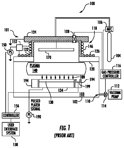
A plasma processing apparatus and method are disclosed which create a uniform plasma within an enclosure.
US 8,659,239 B2 · Assignee: Richtek Technology Corporation · Inventors: Liao; Chia-Wei et al.
Sheet 1 of 19 from the published document. All sheets in the USPTO PDF
The present invention discloses a circuit and a method for providing absolute information for floating grounded integrated circuit. The method includes: receiving an absolute information sense signal carrying absolute information; converting the absolute information sense signal to a current signal; and generating an internal reference signal according to the current signal, wherein the internal reference signal or a relationship between the internal reference signal and a floating ground level is related to the absolute information.
For an IC to operate, it requires a high operation level (often expressed as VDD) and a ground level (often expressed as VSS or GND). In a normal case, the ground level is 0V, a fixed level, such as in the prior art shown in FIG. 1, the ground pin GND is connected to ground (0V). However in certain case, in order to reduce the voltage difference between the high operation level and the ground level such that internal devices of the IC do not require a high specification, a floating grounded IC is proposed. Referring to FIG. 2 which shows an LED (light emitting diode) driver circuit, wherein a power transistor Q, a diode DF and an inductor L forms a buck power conversion circuit; the IC 100 controls the operation of the power transistor Q to convert an input voltage Vin across an input capacitor Cin to an output voltage Vout stored in an output capacitor Cout, and the output voltage Vout
1 of 19 drawing sheets so far from the published document, cropped to the drawing. Every sheet is in the USPTO PDF.
What the patent claimed, word for word. All of it is now free to use.
The present invention relates to a circuit and a method for providing absolute information for a floating grounded integrated circuit (IC).
For an IC to operate, it requires a high operation level (often expressed as VDD) and a ground level (often expressed as VSS or GND). In a normal case, the ground level is 0V, a fixed level, such as in the prior art shown in FIG. 1, the ground pin GND is connected to ground (0V). However in certain case, in order to reduce the voltage difference between the high operation level and the ground level such that internal devices of the IC do not require a high specification, a floating grounded IC is proposed. Referring to FIG. 2 which shows an LED (light emitting diode) driver circuit, wherein a power transistor Q, a diode DF and an inductor L forms a buck power conversion circuit; the IC 100 controls the operation of the power transistor Q to convert an input voltage Vin across an input capacitor Cin to an output voltage Vout stored in an output capacitor Cout, and the output voltage Vout is provided to LEDs. A sense resistor Rcs generates a current sense signal which is fed back to the IC for controlling the current through the LEDs. In this prior art, the ground pin VSS is connected to a node PH. When the power transistor Q is turned ON, the voltage at the node PH is equal to the input voltage Vin minus a voltage drop caused by the on-resistance of the power transistor Q and the sense resistor Rcs, and when the power transistor Q is turned ON, the voltage at the node PH is equal to 0V minus the voltage drop caused by the diode DF, so the voltage at the node PH is not at a fixed level, and therefore the ground level VSS of the IC is floating. In the following context of this specification, in order for the terms to express clear meanings, the reference GND is used for indicating an absolute ground level, while the reference VSS is used for indicating a floating ground level (even though VSS is often used for indicating an absolute ground level in the technical field of this invention, this term VSS will be used dedicatedly for indicating a floating ground level in the following context of this specification).
Although the prior art shown in FIG. 2 can reduce the voltage difference between the high operation level and the ground level, it has a problem that the IC is applied to a system which controls the IC by, or transmits to the IC, signals operating with reference to the absolute ground. (In the following context of this specification, such signals which operate with reference to the absolute ground will be referred to as "absolute signals". Such absolute signals for example may be an analog or digital control signal or a series of control signals, or one or more voltage levels.) The prior art floating grounded IC can not handle these control signal (s) or voltage level (s).
In view of the above, the present invention a circuit and a method for providing absolute information for a floating grounded IC to solve the problem in the prior art, such that a floating grounded IC can recognize information carried by an absolute signal such as control information or a voltage level (referred to hereinafter as "absolute information"), but does not require a complicated circuit or processing steps.
The objective of the present invention is to provide a circuit and a method for providing absolute information for a floating grounded IC.
To achieve the above and other objectives, in one aspect, the present invention discloses a method for providing absolute information for a floating grounded IC, the IC operating between a high operation level and a floating ground level, the method comprising: receiving an absolute information sense signal carrying absolute information; converting the absolute information sense signal to a current signal; and generating an internal reference signal according to the current signal converted from the absolute information sense signal, wherein the internal reference signal or a relationship between the internal reference signal and the floating ground level is related to the absolute information.
In another aspect, the present invention discloses a circuit for providing absolute information for a floating grounded IC, the IC operating between a high operation level and a floating ground level, the circuit for providing absolute information comprising: a transistor having a current inflow end, a current outflow end and a control end, one of the current inflow end and the current outflow end receiving an absolute information sense signal carrying absolute information related to an absolute level, the control end receiving a control voltage, so as to generate a current signal at the current inflow end; and an internal reference signal generation circuit providing the control voltage to control the transistor, and generating an internal reference signal according to the current signal, wherein the internal reference signal or a relationship between the internal reference signal and the floating ground level is related to the absolute information.
The internal reference signal can be used for providing at least one of the following functions: dimming control; reproducing a waveform of an input voltage with reference to an absolute ground level; tri-electrode alternating current (TRIAC) dimming; determining timing to fire TRIAC; adjusting a dimming ratio of TRIAC dimming; under voltage lock out; differentiating high line or low line input; power factor correction; boundary conduction control; and dimming control by an alternating current (AC) power switch.
In one embodiment, the internal reference signal is in current form and has a value equal to or proportional to the current signal.
In another embodiment, the internal reference signal generation circuit converts the current signal to a voltage proportional to the current signal and adds the voltage to the floating ground level to generate the internal reference signal.
In one embodiment, the control voltage controlling the transistor is the high operation level or the floating ground level.
In one embodiment, the transistor is formed in a substrate and it includes: a body of a first conductivity type, located below a surface of the substrate; a gate located above the substrate, for receiving a gate voltage; a source and a drain of a second conductivity type, located in the body and at two sides of the gate; a body electrode of a first conductivity type, located in the body and coupled to the source, for receiving the absolute information sense signal together with the source.
In another embodiment, the transistor is formed in a substrate and it includes: an isolated collector region of a first conductivity type, located below a surface of the substrate; a collector electrode of a first conductivity type, located in the isolated collector region; a base region of a second conductivity type, located in the isolated collector region; a base electrode of a second conductivity type, located in the base region; and an emitter electrode of a first conductivity type, located in the base region.
In yet another embodiment, the transistor is formed in a substrate and it includes: an isolated base region of a first conductivity type, located below a surface of the substrate; a base electrode of a first conductivity type, located in the base region; a collector electrode of a second conductivity type, located in the base region; and an emitter electrode of a second conductivity type, located in the base region. Preferably, the transistor further comprises a high concentration doped region of a first conductivity type below the base region.
In one embodiment, the absolute information sense signal is generated by a dimming circuit according to a dimming signal.
In one embodiment, the circuit for providing absolute information for a floating grounded IC preferably further comprises a low pass filter or a peak detector coupled to the internal reference signal generation circuit, to generate a direct current (DC) signal according to the internal reference signal.
The objectives, technical details, features, and effects of the present invention will be better understood with regard to the detailed description of the embodiments below.
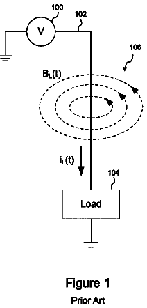
FIG. 1 shows a schematic diagram of a prior art IC having a ground pin GND connected to an absolute ground level (0V).
FIG. 2 shows another prior art IC having a ground VSS connected to a floating ground level.
FIG. 3 shows a first embodiment of the present invention.
FIG. 4A shows an embodiment of the absolute signal sense circuit 13 according to the present invention.
FIG. 4B shows an embodiment of the transistor 131 in FIG. 4A.
FIG. 4C shows another embodiment of the absolute signal sense circuit 13 according to the present invention.
FIG. 4D shows an embodiment of the transistor 131 in FIG. 4C.
FIGS. 5A-5L show several other embodiments of the absolute signal sense circuit 13.
FIG. 6 shows another embodiment of the present invention.
FIG. 7 shows an embodiment of the present invention which is applied to dimming control.
FIGS. 8A-8C show several embodiments of the dimming circuit 19 when the dimming signal Dim is a pulse width modulation (PWM) signal.
FIGS. 8D-8G show several embodiments of the dimming circuit 19 when the dimming signal Dim is an analog signal.
FIG. 8H shows an example of a voltage controlled current source.
FIGS. 9A-9C illustrate that the present invention can reproduce a waveform of an input voltage with reference to the absolute ground level, and obtain a substantially similar waveform NSDC_a or a DC level NSDC_b, to be used for functions which require such information.
FIGS. 10A-10C illustrate an example as to how the present invention is applied to controlling a timing to fire TRIAC dimming.
FIGS. 11A-11D illustrate an example as to how the present invention is applied to adjusting the ratio of TRIAC dimming.
FIG. 12A illustrates an example as to how the present invention is applied to performing under voltage lock out.
FIG. 12B illustrates an example as to how the present invention is applied to differentiating high line and low line inputs.
FIGS. 13A-13D illustrate an example as to how the present invention is applied to power factor correction.
FIGS. 14A-14H show examples of power stages of several power conversion circuits.
FIGS. 15A-15C show that the power conversion circuit is operating in continuous conduction mode (CCM), boundary conduction mode (BCM) and discontinuous conduction mode (DCM), respectively.
FIGS. 16A-16F illustrate an example as to how the present invention is applied to detecting DCM and operating the power conversion circuit towards BCM.
FIGS. 17A-17C illustrate an example as to how the present invention is applied to controlling LED brightness by an AC switch.
FIGS. 18-19 show two other embodiments of the present invention.
FIG. 20A shows another embodiment of the absolute signal sense circuit 13 according to the present invention.
FIG. 20B shows an embodiment of the transistor 151 in FIG. 20A.
FIG. 20C-20F show several other embodiments of the absolute signal sense circuit 13 according to the present invention.
FIG. 21A-21C illustrate that the internal reference signal PSO is also capable of reproducing a waveform of an input voltage with reference to an absolute ground level, and after it is filtered or after peak detection, a substantially similar waveform PSDC_a or a DC level PSDC_b can be obtained, to be used for functions which require such information.
FIG. 22A shows another embodiment of the absolute signal sense circuit 13 according to the present invention.
FIGS. 22B-22C show two embodiments of the transistor 151 in FIG. 22A.
FIG. 22D-22G show several other embodiments of the absolute signal sense circuit 13 according to the present invention.
For better comparison with the prior art, the present invention will be explained using an LED driver circuit as an example, but it should be understood that the spirit of the present invention can be applied to any IC operating with reference to a floating ground level, not limited to an LED driver circuit.
Referring to FIG. 3, the IC 200 is an LED driver circuit for example, which includes a switch control circuit 11, a driver gate 15, and an error amplifier 17. The error amplifier 17 generates an error amplified signal according to a voltage across a sense resistor Rcs, and inputs the error amplified signal to the switch control circuit 11. The switch control circuit 11 generates a power transistor control signal according to the error amplified signal, which is outputted through the driver gate 15 to control a power transistor Q. The power transistor Q operates to convert an input voltage Vin to an output voltage Vout, such that the LED devices are supplied with a necessary current.
The objective of the present invention is to provide absolute information to a floating grounded IC. In general, the input voltage Vin with reference to the absolute ground level is a useful absolute signal. In the shown embodiment, the ground pin VSS of the IC 200 is connected to the node PH, so the IC 200 operates with reference to a floating ground level. When the power transistor Q is on, the floating ground level VSS is about equal to the input voltage Vin (the voltage drop caused by the on-resistance of the power transistor Q and the sense resistor Rcs can be ignored); when the power transistor Q is off, the floating ground level VSS is about equal to 0V (the voltage drop caused by the diode at the lower left can be ignored). Because the floating ground level VSS switches between about the input voltage Vin and about the absolute ground level, the absolute information carried by the input voltage Vin (an absolute signal with reference to the absolute ground level) can be extracted according to the voltage difference between the floating ground level VSS and the absolute ground level, or according to the voltage difference between the floating ground level VSS and the input voltage Vin. In addition, because during operation, there is a fixed voltage difference between the high operation level VDD of the IC and the floating ground level VSS (such voltage difference may be different values indifferent applications), the absolute information carried by the input voltage Vin (an absolute signal with reference to the absolute ground level) also can be extracted according to the voltage difference between the high operation level VDD and the input voltage Vin, or according to the voltage difference between the high operation level VDD and the absolute ground level. However, please note that the present invention can extract information from other absolute signals, not limited to the input voltage Vin. The absolute signal can be a voltage level or a control signal in any form (such as a PWM signal, which will be explained by examples later).
In order to obtain the absolute information, a feature of the present invention is that the IC further includes an absolute signal sense circuit 13. In the embodiment of FIG. 3, the absolute signal sense circuit 13 obtains a sense signal NS carrying absolute information from outside the IC 200 through an absolute signal sense pin Pns, and converts the sense signal NS to an internal reference signal NSO inside the IC 200. The absolute information sense signal NS carries absolute information, i.e., information with reference to an absolute level; in this embodiment, the absolute level is the absolute ground level 0V, and the absolute information sense signal NS is a current signal proportional to a voltage difference between the floating ground level and the absolute ground level. As stated above, the voltage difference between the floating ground level and the absolute ground level carries absolute information of the input voltage Vin with reference to the absolute ground level. Details of the above will be more clearly understood from the embodiments of the absolute signal sense circuit 13. The internal reference signal NSO is a reference signal with reference to the floating ground level VSS (the voltage level at the node PH). The internal reference signal NSO corresponds to the absolute information sense signal NS (the two signals can be equal in value, in proportion, or one being a function of the other). That is, the internal reference signal NSO or a relationship between the internal reference signal NSO and the floating ground level VSS, carries information of the absolute information sense signal NS, or equally speaking, the absolute information carried by the absolute information sense signal NS, is converted to the internal reference signal NSO or a relationship between the internal reference signal NSO and the floating ground level VSS. The internal reference signal NSO can be a current signal or a voltage signal. The IC 200 can perform many functions according to this internal reference signal NSO, such as adjusting the brightness of the LEDs (dimming), controlling the power conversion to be in boundary conduction mode, etc. (applications will be described later). It is shown in the figure that the absolute signal sense pin Pns is connected to an external resistor, but this does not mean that the absolute signal sense pin Pns must be connected with a resistor. It only intends to mean that the absolute signal sense pin Pns obtains the absolute information sense signal NS from outside the IC 200. The absolute information sense signal NS can be provided by any means depending on circuit designs and applications. The absolute information sense signal NS can be a current signal or a voltage signal.
Several examples of the absolute signal sense circuit 13 will be described below. Referring to FIG. 4A, the absolute signal sense circuit 13 includes a transistor 131 and an internal reference signal generation circuit 132. The transistor 131 is shown to be a MOSFET (metal-oxide semiconductor field effect transistor) as an example; however, the transistor 131 can be another type of FET such as a MESFET (metal-semiconductor field effect transistor) or a JFET (junction field effect transistor), or a BJT (bipolar junction transistor). The control end of the transistor 131 (the gate of a FET, or the base of a BJT) receives a control voltage VC, so that the transistor 131 generates a current Is at its current inflow end or current outflow end (the source or drain of a FET, or the collector or emitter of a BJT). The current Is corresponds to the absolute information sense signal NS; it is a current proportional to a voltage difference between the floating ground level and the absolute ground level. It should be explained here that it is conceptually the same either the current Is is generated at the current inflow end or the current outflow end. For a FET, the current at the current outflow end is equal to the current at the current inflow end; for a BJT, although there is a difference between the current at the current outflow end and the current at the current inflow end, which difference is the base current, generally such base current can be ignored and the current at the current outflow end and the current at the current inflow end can be deemed as about the same. The internal reference signal generation circuit 132 provides the control voltage VC to control the transistor 131, and converts the current Is to the internal reference signal NSO. The internal reference signal NSO can be a current signal having a value equal to the current Is, or a voltage or current signal converted from the current Is. After the current Is is converted to the internal reference signal NSO, the IC 200 can safely uses this internal reference signal NSO without concerns such as that the current signal might generate a high voltage to affect or damage a circuit device.
One preferred embodiment of the transistor 131 is shown in FIG. 4B. As shown in the figure, the transistor 131 is for example an NMOS transistor, which comprises: a P type body 13P formed by a P-well, the P-well being encompassed by an N-well 13N in horizontal direction and an N type buried layer or deep well 13L below; an N type heavily doped drain 13D and an N type heavily doped source 13S formed in the P type body 13P; a P type heavily doped body electrode 13B formed in the P type body 13P; and a gate 13G above the substrate. The N type buried layer or deep well 13L for example can be connected to a high voltage VNBL, and in this case the gate voltage VC of the transistor 131 is preferably smaller than this high voltage VNBL plus the threshold voltage Vt of the transistor 131 plus the PN junction forward bias voltage Vf between the P type body 13P and the N type buried layer or deep well 13L, that is, preferably, VC<VNBL+Vt+Vf.
There are various ways for the internal reference signal generation circuit 132 to convert the current Is to the internal reference signal NSO such that the internal reference signal NSO or a relationship between the internal reference signal NSO and the floating ground level VSS is related to the absolute information carried by the absolute information sense signal NS. Several examples of the internal reference signal generation circuit 132 are shown in FIGS. 5A-5F.
In FIG. 5A, the current from the current source at the left generates the control voltage VC with reference to the floating ground level VSS through the drain and gate of the left transistor. Thus, the current Is is generated in the transistor 131 at the right because of the control voltage VC. If the characteristics of the transistor 131 is properly designed, for example by controlling the sensitivity of the gate to source voltage Vgs to current such that the transistor has a low Vgs-to-current sensitivity, the source of the transistor 131 will be similar to a voltage follower following the voltage level of the floating ground level VSS, so that a corresponding relationship between the voltage level of the absolute signal sense pin Pns and the floating ground level VSS is established. By providing a device or circuit between the absolute signal sense pin Pns and an absolute signal (such as the absolute ground level GND), the device or circuit converting the voltage difference between the pin Pns and the absolute signal to a current, the current (which is the current Is) can be used to indicate the relationship between the voltage level of the absolute signal sense pin Pns and the absolute signal, and this also indicates the relationship between the floating ground level VSS and the absolute signal because the voltage level of the absolute signal sense pin Pns corresponds to the floating ground level VSS. The device or circuit between the absolute signal sense pin Pns and the absolute signal can be, for example but not limited to, a resistor. Because the floating ground level VSS switches between about the input voltage Vin and the absolute ground level, the relationship between the floating ground level VSS and the absolute signal includes information about the relationship between the input voltage Vin and the absolute signal, and information about the relationship between the absolute signal and the absolute ground level; such information can be extracted or used by proper means. In brief, the voltage difference between the absolute signal sense pin Pns and an absolute signal (such as the absolute ground level GND) can be converted to the current Is so that the current Is carries absolute information, and in this embodiment, the absolute information sense signal NS is the current Is. The internal reference signal generation circuit 132 converts the absolute information sense signal NS to the internal reference signal NSO having a value equal to the current Is, but is safely readable by a circuit inside the IC.
In FIG. 5B, the internal reference signal NSO is a voltage signal which is equal to the high operation level VDD minus a voltage across the resistor in the figure, and the voltage across the resistor is equal to the current Is multiplied by the resistance of the resistor. Because the relationship between the high operation level VDD and the floating ground level VSS is fixed, the relationship between the internal reference signal NSO and the floating ground level VSS is related to the absolute information carried by the absolute information sense signal NS; in other words, the absolute information carried by the absolute information sense signal NS is converted to the relationship between the internal reference signal NSO and the floating ground level VSS.
FIG. 5C is similar to FIG. 5A, in which the internal reference signal NSO is a current signal, which is the current flowing from the PMOS transistor at the right. Note that the current mirror at the right can have any current replication ratio as desired, that is, the internal reference signal NSO does not need to have a value exactly equal to the current Is, but can be proportional to the current Is (i.e., the internal reference signal NSO can be a multiple or fraction of the current Is in number).
In FIGS. 5D-5F, the control end of the transistor 131 (the gate of a FET or the base of a BJT) receives the floating ground level VSS. In FIG. 5D, the internal reference signal generation circuit 132 is only required to provide the floating ground level VSS to the gate of the transistor 131. In this embodiment, the current Is is related to the gate to source voltage Vgs of the transistor 131, or, if a resistive device is connected between the pin Pns and the absolute signal, the current Is is related to the voltage across the resistive device; thus, the current Is is related to the voltage difference between the floating ground level VSS and the absolute signal. In other words, the internal reference signal NSO itself (having a value equal to the current Is in this embodiment) carries the information of the absolute information sense signal NS, and this means that the absolute information carried by the absolute information sense signal NS is converted to the content of the internal reference signal NSO.
FIGS. 5E and 5F are similar to FIGS. 5B and 5C respectively, except that the control voltage of the transistor 131 is changed from Vgs+VSS to VSS. In these embodiments, the internal reference signal NSO itself or the relationship between the internal reference signal NSO and the floating ground level VSS is related to the absolute information carried by the absolute information sense signal NS, that is, the absolute information carried by the absolute information sense signal NS is converted to the content of the internal reference signal NSO or the relationship between the internal reference signal NSO and the floating ground level VSS.
The transistor 131 is not necessarily a MOSFET; it can be any other type of transistor, such as a JFET, etc. Another embodiment of the transistor 131 is shown in FIG. 4C, which is a BJT having a control end (base) receiving the control voltage VC, to generate the current Is at its current inflow end (collector), wherein the current Is is related to the absolute information sense signal NS. The BJT can be embodied for example as the semiconductor structure shown in FIG. 4D, wherein the transistor 131 is formed in a P type substrate or a P type well formed by any suitable process; the transistor 131 includes an N type collector region located below a surface of the substrate and isolated by a P type region; an N type collector electrode located in the N type collector region; a P type base region located in the N type collector region; a P type base electrode in the P type base region; and an N type emitter region in the P type base region.
FIGS. 5G-5L show several examples illustrating how the internal reference signal generation circuit 132 cooperates with the BJT to convert the absolute information sense signal NS to the internal reference signal NSO. These circuits function in a similar way to FIGS. 5A-5F, and therefore detail explanation thereof is omitted. FIGS. 5I and 5L shows that the current mirror circuit in the figure can be formed by FETs or BJTs as equivalents. Similarly, the current mirror circuit in FIGS. 5C and 5F can be formed by BJTs instead.
In FIG. 3, the power (high operation level) VDD of the IC 200 is provided by the voltage across the capacitor CVDD, but when the circuit is starting up, there are not enough charges accumulated in the capacitor CVDD. To solve this, a start-up resistor Rst can be provided between the input voltage Vin and the high operation level VDD, to provide a start-up voltage to the IC 200. However, this is not the only way to provide the start-up voltage; as shown in FIG. 6, the start-up voltage can be provided by other means, not necessarily from the input voltage Vin through the resistor Rst.
In the prior art of FIG. 2, because the ground level is floating, it can not perform functions which require absolute information. In the present invention, because the IC can recognize the information expressed by an absolute signal (such as a control signal or a voltage level), the IC can perform functions which require absolute information. Several examples of such functions that the present invention can be applied to are explained below.
Application: Dimming Control
One function which requires absolute information is the dimming control to adjust the LED brightness. The dimming signal for controlling an LED driver circuit, either in PWM form or analog form, is an absolute signal with reference to the absolute ground level. Therefore, a floating grounded LED driver circuit must know the absolute information carried by such absolute signal so that it can perform dimming control. FIG. 7 shows an embodiment of the present invention which is applied to dimming control. The dimming circuit 19 receives a dimming signal Dim, and converts the dimming signal Dim to the absolute information sense signal NS which is inputted to the inside of the IC 200. The IC 200 can adjust the on-time or duty ratio of the power transistor Q according to the absolute information sense signal NS, so as to adjust the brightness of the LED devices.
More specifically, the dimming signal can be in PWM form or analog form (but in both cases it is an absolute signal with reference to the absolute ground level); FIGS. 8A-8C show several embodiments of the dimming circuit 19 when the dimming signal Dim is a PWM signal. In FIG. 8A, the dimming circuit 19 converts the PWM dimming signal Dim to the absolute information sense signal NS which is also in PWM form. In FIG. 8B, the absolute signal sense circuit 13 converts the absolute information sense signal NS in PWM form to the internal reference signal NSO which is also in PWM form. A low pass filter LPF converts the internal reference signal NSO to an analog signal. FIG. 8C shows that the low pass filter LPF can be integrated in the dimming circuit 19 such that the absolute information sense signal NS generated by the dimming circuit 19 is an analog signal.
FIGS. 8D-8G show several embodiments of the dimming circuit 19 when the dimming signal Dim is an analog signal. In FIG. 8D, the dimming circuit 19 is a voltage controlled resistor, which in one embodiment can be a transistor, and it converts the analog dimming signal Dim to the absolute information sense signal NS which is also in analog form. In FIG. 8E, the dimming circuit 19 is a voltage controlled current source, which in one embodiment can be a circuit as shown in FIG. 8H, and it also converts the analog dimming signal Dim to the absolute information sense signal NS in analog form. In FIG. 8F, the dimming circuit 19 includes a resistor and a voltage controlled voltage source, the latter in one embodiment being a circuit as shown by the dash line in FIG. 8G, and the dimming circuit 19 in this embodiment also converts the analog dimming signal Dim to the absolute information sense signal NS in analog form.
The absolute information sense signal NS generated by the dimming circuit 19 in FIGS. 8A-8F can be converted to the internal reference signal NSO by the absolute signal sense circuit 13, so that the floating grounded IC can uses the internal reference signal NSO for dimming control.
Application: Reproducing a Waveform of the Input Voltage with Reference to the Absolute Ground Level
When the input voltage Vin is a signal obtained from an AC signal after bridge rectification, it will present a semi-sinusoidal waveform with reference to the absolute ground level GND, as shown by the first waveform in FIG. 9C. Many functions require to know such waveform of the input voltage Vin with reference to the absolute ground level GND, such as tri-electro AC (TRIAC) dimming, power factor correction (PFC), boundary conduction control, etc. To meet this requirement, the present invention proposes circuits and methods to reproduce the waveform of the input voltage Vin with reference to the absolute ground level GND in a floating grounded IC.
According to the present invention, the absolute signal sense circuit 13 for example can use any of the circuits shown in FIGS. 5D-5F, and a voltage device (such as a resistor) having a voltage proportional to the current Is can be provided between the internal reference signal NSO and the floating ground level VSS. Thus, the relationship between the internal reference signal NSO and the floating ground level VSS can reproduce the relationship between the input voltage Vin and the absolute ground level GND.
More specifically, referring to FIGS. 9A-9C, the absolute signal sense circuit 13 for example uses the circuit of FIG. 5F. When the power transistor Q is on, the floating ground level VSS is about equal to the input voltage Vin (referring to FIGS. 3, 6 and 7, the voltage drop caused by the on-resistance of the power transistor Q and the sense resistor Rcs can be ignored); when the power transistor Q is off, the floating ground level VSS is about equal to 0V (the voltage drop caused by the diode can be ignored). Hence, the floating ground level VSS (with reference to the absolute ground level GND) has a waveform as shown by the second waveform in FIG. 9C. When the power transistor Q is on, the transistor 131 is on, the voltage at the absolute signal sense pin Pns is equal to the floating ground level VSS minus the gate to source voltage difference of the transistor; when the power transistor Q is off, the voltage at the absolute signal sense pin Pns is about equal to the absolute ground level GND. Therefore, the voltage at the absolute signal sense pin Pns with reference to the absolute ground level GND has a waveform as shown by the third waveform in FIG. 9C. When the transistor 131 is on, it generates the current Is; when the transistor 131 is off, the current Is is zero. Therefore, the current Is has a waveform as shown by the fourth waveform in FIG. 9C. The internal reference signal NSO is equal to the floating ground level VSS plus the voltage across the resistor 133, and the voltage across the resistor 133 is equal to the current Is multiplied by the resistance of the resistor 133, so the internal reference signal NSO (with reference to the floating ground level VSS) has a waveform as shown by the fifth waveform in FIG. 9C, which reproduces the relationship between the input voltage Vin and the absolute ground level GND.
Application: Reproducing a Waveform of the Input Voltage with Reference to the Absolute Ground Level in TRIAC Dimming
TRIAC dimming adjusts the turn-on angle of an AC signal; referring to the waveform at the upper right of FIG. 9C, in TRIAC dimming, a portion of the on-time is cut off. The fifth waveform at the right of FIG. 9C shows that the internal reference signal NSO can reproduce the waveform of the input voltage Vin after TRIAC dimming adjustment.
FIGS. 9A-9B show embodiments wherein the internal reference signal NSO passes through a low pass filter LPF (FIG. 9A) or a peak detector 137 (FIG. 9B) so that the internal reference signal NSO in ringing shape is converted to a direct current (DC) signal NSDC in analog form. Depending on the requirement to use the DC signal and the bandwidth design of the low pass filter LPF or the peak detector 137, the generated DC signal NSDC can substantially reproduce the waveform of the input voltage Vin with reference to the absolute ground level GND (as shown by the sixth waveform NSDC_a in FIG. 9C), or the generated DC signal NSDC can be a DC level (as shown by the seventh waveform NSDC_b in FIG. 9C, NSDC_b is an average value when the low pass filter LPF is used, or a peak value if the peak detector 137 is used).
Application: Determining Timing to Fire the TRIAC Dimming
In general, to perform TRIAC dimming function, there must be a minimum loading. Such minimum loading can be achieved by, for example:
increasing the current upper limit of a power conversion circuit;
switching the power conversion circuit to operate in a current mode having a constant peak (or valley) value, or in a hysteresis mode having a higher current level;
forcing the power transistor of the power conversion circuit to operate in a higher duty ratio;
switching the power conversion circuit to operate in a constant-on-time mode with a longer on time, or
other ways. The above actions to reach the minimum loading (i.e., to fire or initiate TRIAC dimming) should be taken at an earlier stage of the semi-sinusoidal waveform of the input voltage Vin, but not too early lest the voltage would be too low. In view of the above, the present invention discloses an embodiment for determining the timing to fire TRIAC dimming, which is explained with reference to FIGS. 10A-10C.
As shown in FIG. 10A, because the waveform NSDC_a reproduces the waveform of the input voltage Vin with reference to the absolute ground level GND, according to the present invention, the waveform NSDC_a can be inputted to a hysteresis comparator 138 and a comparator 139. The hysteresis comparator 138 compares the waveform NSDC_a with a reference level VTH, wherein the hysteresis zone of the hysteresis comparator 138 is .DELTA.V; the comparator 139 compares the waveform NSDC_a with an under voltage lock out reference level VUVLO. Referring to FIGS. 10A-10C, when the waveform NSDC_a has a level lower than the under voltage lock out reference level VUVLO, the comparator 139 generates a high level under voltage lock out signal UVLO, indicating that the voltage is too low, so the circuit should not fire TRIAC dimming (OFF). When the waveform NSDC_a has a level higher than the under voltage lock out reference level VUVLO, the comparator 139 generates a low level under voltage lock out signal UVLO; if the level of the waveform NSDC_a is lower than the reference level VTH, it means that the timing is at an earlier stage of the semi-sinusoidal waveform, so it is a good timing for the circuit to fire TRIAC dimming. However, if the level of the waveform NSDC_a is higher than the reference level VTH, it means that the semi-sinusoidal waveform of the input voltage Vin has passed its earlier stage, so the circuit should enter normal operation mode (NOM). When the waveform NSDC_a becomes lower than the reference level VTH, because it is not below the hysteresis zone .DELTA.V, the output of the hysteresis comparator 138 does not switch level; the circuit is still in the normal operation mode. When the waveform NSDC_a is again lower than the under voltage lock out reference level VUVLO, the circuit enters the OFF stage again.
Application: Adjusting the Dimming Ratio of TRIAC Dimming
The description continues in the full USPTO document.
About 6,695 words. The USPTO PDF has it with every drawing.
Fees are due 3.5, 7.5 and 11.5 years after grant. This patent expired on February 25, 2026, so the fee marked "not paid" was the one that went unpaid.
CIRCUIT AND METHOD FOR PROVIDING ABSOLUTE INFORMATION FOR FLOATING GROUNDED INTEGRATED CIRCUIT
Filed Jul 2011 · published Jul 2012Circuit and method for providing absolute information for floating grounded integrated circuit
Filed Jul 2011 · granted Feb 2014Earlier publications, parents and continuations. None of them can still be enforced, or this patent would not be listed.
Prior art cited by the examiner or applicant. Useful when you check your own idea for novelty.
Everything on this page comes from the documents linked above.