 Lapsed, fee not paid9 drawings
Software & Apps · US 8,645,618 B2
Flexible flash commands
A method of controlling a flash media system.
US 8,645,623 B1 · Assignee: EMC Corporation · Inventors: O'Shea; John et al.
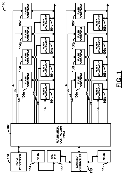
Sheet 1 of 49 from the published document. All sheets in the USPTO PDF
A data storage system having protocol controller for converting packets between PCIE format used by a storage processor and Rapid IO format used by a packet switching network. The controller includes a PCIE end point for transferring atomic operation (DSA) requests, a data pipe section having a plurality of data pipes for passing user data; and a message engine section for passing messages among the plurality of storage processors. An acceleration path controller bypasses a DSA buffer in the absence of congestion on the network. Packets fed to the PCIE end point include an address portion having code indicating an atomic operation. An encoder converts the code from a PCIE format into the same atomic operation in SRIO format. Each one of a plurality of CPUs is adapted to perform a second DSA request during execution of a first DSA request.
As is known in the art, large host computers and servers (collectively referred to herein as "host computer/servers") require large capacity data storage systems. These large computer/servers generally include data processors, which perform many operations on data introduced to the host computer/server through peripherals including the data storage system. The results of these operations are output to peripherals, including the storage system. One type of data storage system is a magnetic disk storage system having a bank of disk drives. The bank of disk drives and the host computer/server are coupled together through a system interface. The interface includes "front end" or host computer/server controllers (or storage processors) and "back-end" or disk controllers (or storage processors). The interface operates the storage processors in such a way that they are transparent to the host c
1 of 49 drawing sheets so far from the published document, cropped to the drawing. Every sheet is in the USPTO PDF.
What the patent claimed, word for word. All of it is now free to use.
This invention relates generally to data storage systems and more particularly to data storage systems having a host computer/server coupled to a bank of disk drives through a system interface, such interface having a plurality of storage processors (SPs) interconnected by a packet switching network.
As is known in the art, large host computers and servers (collectively referred to herein as "host computer/servers") require large capacity data storage systems. These large computer/servers generally include data processors, which perform many operations on data introduced to the host computer/server through peripherals including the data storage system. The results of these operations are output to peripherals, including the storage system.
One type of data storage system is a magnetic disk storage system having a bank of disk drives. The bank of disk drives and the host computer/server are coupled together through a system interface. The interface includes "front end" or host computer/server controllers (or storage processors) and "back-end" or disk controllers (or storage processors). The interface operates the storage processors in such a way that they are transparent to the host computer/server. That is, user data is stored in, and retrieved from, the bank of disk drives in such a way that the host computer/server merely thinks it is operating with its own local disk drive. One such system is described in U.S. Pat. No. 5,206,939, entitled "System and Method for Disk Mapping and Data Retrieval", inventors Moshe Yanai, Natan Vishlitzky, Bruno Alterescu and Daniel Castel, issued Apr. 27, 1993, and assigned to the same assignee as the present invention.
As described in such U.S. Patent, the interface may also include, in addition to the host computer/server storage processors and disk storage processors, a user data semiconductor global cache memory accessible by all the storage processors. The cache memory is a semiconductor memory and is provided to rapidly store data from the host computer/server before storage in the disk drives, and, on the other hand, store data from the disk drives prior to being sent to the host computer/server. The cache memory being a semiconductor memory, as distinguished from a magnetic memory as in the case of the disk drives, is much faster than the disk drives in reading and writing data. As described in U.S. Pat. No. 7,136,959 entitled "Data Storage System Having Crossbar Packet Switching Network", issued Nov. 14, 2006, inventor William F. Baxter III, assigned to the same assignee as the present invention, the global cache memory may be distributed among the service processors.
Another data storage system is described in U.S. Patent Application Publication No. US 2005/0071424, entitled DATA STORAGE SYSTEM, inventor Baxter III, published Mar. 31, 2005, assigned to the same assignee as the present invention. In such system, front and back end directors (hereinafter referred to as storage processors) include: a message engine, a data pipe and a portion of a global cache memory. The front and back end storage processors are interconnected through a packet switching network. The packet switch network passes both user data and messages, the user data passing through the data pipe and the messages being generated and received by the message engine. Write data supplied by the host computer/server for storage in the bank of disk drives is passed to the local cache memory section of one of the second plurality of storage processor/memory boards and the storage processor on such one of the second plurality of storage processor/memory boards controls the transfer of data from such one of the memory sections to the bank of disk drives. Read data supplied by the bank of disk drives for use by the host computer/server is passed to the local cache memory section of one of the first plurality of storage processor/memory boards and the storage processor on such one of the first plurality of storage processor/memory boards controls the transfer of data from such one of the memory sections to the host computer/server. The front-end and back-end storage processors control the transfer of user data between the host computer/server and the bank of disk drives through the packet switching networks in response to messages passing between and/or among the storage processors through the packet switching networks.
As is also known in the art, it is desirable to maximize user data transfer through the interface including maximized packet transfer through the packet switching network.
As is also known in the art, each one of the storage processors includes a CPU and a local/remote memory interconnected to the packet switching network through commercially available root complex, such as an INTEL root complex using a PCI-Express (PCIE) protocol. One such packet switching network operates with a Serial Rapid IO (SRIO) protocol and is sometimes referred to as an SRIO fabric. We have discovered that for certain system interfaces, greater system throughput can be achieved using an SRIO fabric. The benefits of SRIO over other packet switched protocols such as Ethernet for storage applications is that SRIO has guaranteed delivery (since every request has associated response), supports low latency applications (since maximum packet payload size is 256 bytes) while maintaining reasonable bandwidth (of about 1 Gbyte/sec per direction), and can be implemented in a low cost, structured ASIC designs since protocol complexity is minimal.
It should be noted that some SRIO terminology used herein may be found in the following references published by the RapidIO Trade Association: Rapid IO Interconnect Specification, version 1.3 Rapid IO Interconnect Specification, Part VI: Physical Layer 1x/4x LP-Serial Specification; some of the PCI terminology used herein may be found in the following references published by the PCI-SIG (Peripheral Component Interconnect Special Interest Group): PCIE Express Base Specification, version 1.1; and other terminology used herein may be found in INCITS: T10 Technical Committee on SCSI Storage Interfaces--Preliminary DIF (Block CRC) documents
As is also known in the art, a DSA transfer is used for a CPU within a storage processor (SP) to indirectly access a local/remote memory in any SP on the packet switching network. More particularly, as used herein, a DSA transfer is "indirect" because in the present system the CPU is "detached" from the operation as soon as the DSA operation is initiated from the CPU. Once initiated, the CPU is free to perform other work (if there is work not dependent on a DSA in flight) until the DSA transfer is completed. When the DSA is completed, the DSA status and data (if applicable) is "pushed" into the initiating, or source SP's local memory and an interrupt generated to the initiating CPU for completion notification. (Polling of the DSA status word in local memory is also possible for absolute lowest latency when no forward progress can be made until the DSA transfer is completed).
However, existing SRIO fabrics do not support DSA or atomic transfers with commercially available root complexes. More particularly, PCI-Express (PCIE) standard does not directly support atomic operations and the RIO standard support for atomic operations is limited.
The details of one or more embodiments of the invention are set forth in the accompanying drawings and the description below. Other features, objects, and advantages of the invention will be apparent from the description and drawings, and from the claims.
FIG. 1 is a diagram of a data storage system having an interface coupled between a host computer/server and a bank of disk drives, such interface having a plurality of storage processors (SPs), one portion of the SPs being coupled to the host computer/server and another portion of the SPs being coupled to the bank of disk drives, the plurality of SPs being interconnected through a pair of packet switching networks according to the invention;
FIG. 1A is a diagram showing master and slave portions of an exemplary pair of the SPs of FIG. 1 interconnected through one of the packet switching networks, one of the SPs being a source SP and the other being a destination SP;
FIG. 1B is a diagram showing master and slave portions of the same one of the SPs of FIG. 1 interconnected through one of the packet switching networks;
FIG. 2 is a block diagram of an exemplary one of a plurality of storage processors used in the data storage system of FIG. 1;
FIG. 3 is a block diagram of a PCIE/SRIO protocol controller used in the storage processor (SP) of FIG. 2 according to the invention;
FIG. 4 is a block diagram of a DSA section used in the PCIE/SRIO protocol controller of FIG. 2 according to the invention;
FIG. 4A is a block diagram of a master DSA pipe used in the DSA section of FIG. 4 according to the invention;
FIG. 4B is a block diagram of a Slave DSA (SDSA) used in the DSA section of FIG. 4 according to the invention;
FIG. 4C is a diagram showing a pair of SPs of FIG. 2 interconnected through a packet switching network, such each of the SPs having a master DSA and a slave DSA of FIGS. 4B and 4C, respectively, according to the invention;
FIG. 4D is shows the primary address format of a packet used in the data storage system of FIG. 1;
FIG. 4E shows a PCI setup packet packetized into an SRIO request packet used in the packet switching network of the system of FIG. 1;
FIG. 4F shows an SRIO response packet packetized into a PCIE status packet used in the packet switching network of the system of FIG. 1;
FIG. 4G shows a PCIE address of a PCIE packet mapped into an SRIO request header used in the packet switching network of the system of FIG. 1;
FIG. 4H shows a DSA cache set up format;
FIG. 4I is a flowchart of an DSA atomic operation performed by the system of FIG. 1 according to the invention;
FIG. 4J is a flowchart of an egress cut-through process performed by the system of FIG. 1 according to the invention;
FIG. 4K shows the flow of an SRIO request packet to a PCIE write/read to an SRIO response packet performed by the system of FIG. 1 according to the invention;
FIG. 4L shows a DSA cache response format used by the system of FIG. 1 according to the invention;
FIG. 4M is a flowchart of the process performed by a slave DSA of FIG. 4B according to the invention;
FIG. 4N is a flowchart of an ingress cut through process used by a DSA of FIG. 4A according to the invention;
FIG. 4O shows an SRIO response header format used by the system of FIG. 1 according to the invention;
FIG. 4P is a flowchart showing a process wherein a plurality of buffers in a DSA buffer section of the DSA of FIG. 4A stores a corresponding one of a plurality of DSA packets and independently transmit such packets from the buffers to the packet switching network a plurality of buffers according to the invention;
FIG. 4Q is a flowchart of a process used by a DSA of FIG. 4A to perform an atomic operation range check according to the invention;
FIG. 5 is a block diagram of a data pipe section used the PCIE/SRIO protocol controller of FIG. 3 according to the invention;
FIG. 5A is a block diagram of an exemplary one of a pair of data pipe groups used in the data pipe section of FIG. 5 according to the invention;
FIG. 5B is a block diagram of an exemplary the other one of a pair of data pipe groups used in the data pipe section of FIG. 5 according to the invention;
FIG. 5C is a diagram showing a pair of SPs of FIG. 2 interconnected through a packet switching network, such each of the SPs having a master data pipe section of FIG. 5D and a slave data pipe section of FIG. 5E according to the invention;
FIG. 5D is a block diagram of the master section of an exemplary one of the I/O data pipes used in the pair of data pipe groups used in the data pipe section of FIG. 5 according to the invention;
FIG. 5E is a block diagram of the slave section of an exemplary one of the I/O data pipes used in the pair of data pipe groups used in the data pipe section of FIG. 5 according to the invention;
FIG. 5F is an overall flowchart of a process used to control the flow of user data through a data pipe of FIG. 5;
FIG. 5G is a more detailed flowchart of a process used to control the flow of user data through a data pipe of FIG. 5;
FIGS. 5H through 5V are flowcharts of individual processes used in the process used to control the flow of user data through a data pipe of FIG. 5;
FIG. 6 is a block diagram of a message engine (ME) used in the PCIE/SRIO protocol controller of FIG. 3 according to the invention;
FIG. 6A is a block diagram of the egress ME portion of the ME of FIG. 6;
FIG. 6B is a block diagram of the ingress ME portion of the ME of FIG. 6;
FIG. 6C shows a ME PCIE outbound packet format used by the ME of FIG. 6;
FIG. 6D shows a ME PCIE inbound packet format used by the ME of FIG. 6;
FIG. 7 is a block diagram of a CPU Access Port (CAP) section through which a CPU used in the PCIE/SRIO protocol controller of FIG. 3 sends maintenance packets according to the invention;
FIG. 7A is a flowchart of the process used by the CAP of FIG. 7;
FIG. 8 is a block diagram of a trace buffer used in the of a PCIE/SRIO protocol controller of FIG. 3;
FIGS. 9A and 9B are block diagrams of an exemplary one of a plurality of routers used in used in the PCIE/SRIO protocol controller of FIG. 3;
FIG. 9C is a flowchart of ingress credit management used by the router of FIG. 9B;
FIG. 9D is a flowchart of ingress credit management used by the router of FIG. 9B;
FIG. 9E shows a packet routing table used by the router of FIG. 9B based on FTYPE/TTYPE for store forward (SF) packets;
FIG. 9F is a flowchart used by an ingress error ring used in the ME ingress of FIG. 6B;
FIG. 9G is a block diagram of the egress arbiter used in the router of FIG. 9; and
FIG. 9H show shuffle codes for the shuffle arbiter of the arbiter of FIG. 9B; and
FIG. 9I shows the contents of an error status used in the ME ingress of FIG. 6B.
Like reference symbols in the various drawings indicate like elements.
Referring now to FIG. 1 a data storage system 100 is shown having a host computer/server 102 coupled to a bank of disk drives 104 through a system interface 106. The system interface 106 includes front end storage processors (SPs) 108 connect to the host computer/server 102 and back end storage processors 108 connected to the bank of disk drives 104. Each one of the SPs 108 and 108 is identical in construction, an exemplary one thereof, here one of the front end SPs 108, being shown in more detail in FIG. 2.
The front end and back end storage processors 108 (FIG. 1) are interconnected through a pair of redundant packet switching networks 112A, 112B. Further, as will be described herein, a global cache memory 114 (FIG. 2) is made up of a plurality of global cache memory sections, each one of the global cache memory sections being distributed in a corresponding one of the front and back end storage processors 108.
The front-end and back-end storage processors 108 (FIG. 1) control the transfer of user data (sometimes referred to as host/server or customer data) between the host computer/server 102 and the bank of disk drives 104 through the packet switching networks 112A, 112B in response to messages passing between and/or among the storage processors 108 through the packet switching networks 112A, 112B. Here, the packet switching networks 112A, 112B transfer packets of user data, messages, maintenance packets and DSA transfers, to be described, using a SRIO protocol.
As noted above, each one of the front end and back end storage processors 108 is identical in construction, an exemplary one thereof being shown in more detail in FIG. 2 to include an I/O module 200 connected via port 109 (FIGS. 1 and 2), in the case of a front end storage processor 108, to the host computer/server 102 and in the case of a back end storage processor 108 connected to the bank of disk drives 104, as indicated in FIG. 1. The I/O module 200 (FIG. 2) is connected to a commercially available root complex 202, here, for example, an Intel root complex. Also connected to the root complex 202 is a CPU section 204 having a plurality of central processing units (CPUs) 206; a local/remote memory 210; and a PCIE/SRIO Protocol Controller 212, to be described in more detail in connection with FIG. 3. Suffice it to say here that the PCIE/SRIO Protocol Controller 212, among other things, converts between the Serial Rapid Input/Output (SRIO) protocol used by the packet switching networks 112A, 112B, and the PCIE protocol used by the CPUs 206, and the I/O module 200. The PCIE/SRIO Protocol Controller 212 is connected to the root complex 202 via port 230 and is connected to pair of packet switching networks 112A, 112B (FIG. 1) via ports 230A, 230B, respectively, as indicated.
The local/remote memory 210 has: a section of a global cache memory 114 (i.e., a cache memory section) as described in the above referenced U.S. Pat. No. 7,136,959, for storing user data; a bank of plurality of descriptor rings 213, here for example 8 pairs of descriptor rings (one of the rings in a pair is a request ring 215 and the other one of the rings is a response ring 217); a message engine ring section 244 which contains inbound message ring 220 (FIG. 2); an outbound message ring 222 (FIG. 2); an error ring 224; a CPU control store section 242 which contains the CPU's instructions and data space; and a store-forward buffer which acts as a temporary buffer for user data from the IO Module 200 before it is moved to global cache memory. Further, while the local/remote memory 210 will be described in more detail, it should first be noted that when the local/remote memory 210 stores in user data section 114 user data for it's own storage processor 108 it may be considered as "local" memory whereas when the local/remote memory is storing user data in section 114 for other ones of the storage processors 108 it may be considered as "remote" memory.
The local/remote attributes are shown to the right of local/remote memory 210 on FIG. 2. The areas of memory that are marked as `local` can only be accessed by the local SP. Remote SP's are blocked from accessing these local data structures to reduce the chance of corruption. The access protection mechanism is described later. Areas of memory that are labeled `local/remote` can be accessed from the local SP or a remote SP over the packet switching network.
The data stored in local/remote memory 210 is also protected from accidental overwrite (and accidental data overlays). End-to-end protection of data from the host to disk in this case is managed with higher level data protections such as T10 standard DIF CRC protection (see INCITS: T10 Technical Committee on SCSI Storage Interfaces--Preliminary DIF (Block CRC) documents) which is supported in the PCIE/SRIO Protocol Controller 212, Data pipe section 500 (FIG. 3, to be described in connection with FIG. 5). Unique LBA (logical block addresses) provide overlay protection while the DIF CRC provides for overwrite protection.
Referring now to FIG. 3, the PCIE/SRIO Protocol Controller 212 is shown in more detail to include a PCIE Express (PCIE) endpoint 300 connected to the root complex 202 (FIG. 2) through port 220 for passing PCIE protocol information between the PCIE/SRIO Controller 212 and the root complex 202. Connected to the PCIE Express (PCIE) endpoint 300 are: a DSA section 400, to be described in more detail in connection with FIG. 4; the data pipe section 500 to be described in more detail in connection with FIG. 5, a message engine 600, to be described in more detail in connection with FIG. 6; a CPU Access Port (CAP) section 700 through which the CPUs send maintenance packets and which will described in more detail in connection with FIG. 7; and a monitoring section 800 having a trace buffer, to be described in more detail in connection with FIG. 8.
Before describing the PCIE End Point 300, it should be noted that message packet, user data packet and maintenance packet transfers from the local/remote memory 210 (FIG. 2) to the PCIE/SRIO Controller 212 are referred to as store forward (SF) transfers and transfers directly from the CPU 204 which by-pass the local/remote memory 210 are low latency or DSA transfers.
Referring now to the PCIE End Point 300, packets sent to the packet switching networks (egress) are fed by the root complex 202 (FIG. 2) to port 220. A Base Address Register (BAR 0) "DSA decoder" 301 examines the packet to determine whether it is a DSA transfer (i.e., DSA request) or a non-DSA transfer. If it is a DSA request, the packet passes directly to a selector 304 and then to port 400P of the DSA section 400. On the other hand, if the decoder 301 determines that the packet is not a DSA request, the packet passes through a buffer 302 and then to the selector 304. The non-DSA packet is then fed to either the message engine 600, the CAP section 700, or the data pipe section 500. For ingress packets from the packet switching networks 112A, 112B to the root complex 202, the packets from the DSA section 400 pass directly to an arbiter 306 and the to port 220 while the non-DSA packets pass to a buffer section 307 prior to passing to the arbiter 306. The arbiter 306 determines if there is ample credit on link 220 (i.e., packet buffer availability in the root complex 202) to send a packet to the root complex 202 and selects between the buffered non-DSA requests and DSA section 400 requests. The DSA section 400 requests are always treated as highest priority to minimize DSA latency. After the arbitration, the selected packet is presented to port 220.
Referring to FIG. 3, the DSA section 400 (FIG. 4) is connected to: the first one of the pair of switching networks 112A via port 230A through an SRIO Router 900A and SRIO "A" end point 1000A; and the second one of the pair of switching networks 112B via port 230B through an SRIO Router 900B and SRIO "B" end point 1000B.
Similarly, the message engine 600 (FIG. 3) is connected to: the first one of the pair of switching networks 112A (FIG. 1) via port 230A through the SRIO Routers 900A, 902A and SRIO "A" end point 1000A, as shown in FIG. 3; and the second one of the pair of switching networks 112B via port 230B through the SRIO Router 900B, 902B and SRIO B end point 1000B.
The CAP section 700, and data pipe section 400 is connected to: the first one of the pair of switching networks 112A via port through the SRIO Router 902A and the SRIO A end point 1000A; and the second one of the pair of switching networks 112B via port 230B through the SRIO Router 902B and SRIO B end point 1000B.
The SRIO "A" and "B" end points 1000A and 1000B are identical, end point 1000A being shown in more detail in FIG. 3 to have two ports; a low latency (LL) port and a store forward (SF) port. The LL ports of end points 1000A, 1000B are connected to ports 400PA and 400PB, respectively of the DSA section 400 through SRIO Router A 900A and SRIO Router B 900B, respectively, as indicated. Reference is made to copending U.S. patent application entitled "PACKET SWITCHING NETWORK END POINT CONTROLLER", inventors Alexander Y. Aronov, Stephen D. MacArthur, Michael Sgrosso, and William F. Baxter III, Ser. No. 11/022,998, filed Dec. 27, 2004, assigned to the same assignee as the present invention the entire contents thereof being incorporated herein by reference.
Considering egress of packets to the packet switching networks, 112A, 112B, the LL port is connected directly to a selector 315 through a LL cut-through path, as indicated, and is also connected to the selector 315 through a store forward (SF) buffer 316, as shown. An arbiter 313 controls the operation of the selector 315. The arbiter 313 selects the LL cut-through path whenever the SF Buffer 316 is empty, and if the transmitter (TX) link (i.e., port 230A, 230B) is idle. If the TX link is not idle, then DSA packets are stored within store forward (SF) buffer 316. The output of the selector 315 is connected to the packet switching network 112A in the case of end point 1000A and packet switching network 112B in the case of end point 1000B, as indicated.
Considering ingress where packets are received from the packet switching networks 112A, 112B, such packets pass to a selector 320 directly and also to such selector 320 through a store forward (SF) buffers 322, as indicated. The selector 320 is controlled by the incoming packet (i.e., the destination ID field contains a low latency (LL), store-forward (SF) path select bit) to pass low latency incoming packets directly to the LL port bypassing SF buffer 322 and to pass store forward packets to the SF port after passing through the SF buffer 322. The ingress packet on the SF port then passes to SRIO Router A 902A or SRIO Router B 902B, as the case may be, and then to the message engine 600, or the data pipe section 500. The ingress packet on the LL port then passes to SRIO Router 900A or SRIO Router 900B, as the case may be, and then to the DSA Section 400.
As noted above, and referring again to FIG. 1, packets are transmitted between storage processors (SPs) 108 through a packet switching network 112A, 112B. Thus, the one of the SPs producing a request packet for transmission may be considered as a source SP 108 and the one of the SPs receiving the transmitted request packet may be considered as the destination SP 108, as shown in FIG. 1A. More particularly, when the request packet is transmitted from the source SP 108 requesting execution of such transmitted packet by the destination SP 108, the components in the source SP 108 are sometimes herein referred to as master components and the components in the destination SP 108 may be considered as a slave components, as shown in FIG. 1A. It is noted from FIG. 1A that any one of the SPs 108 may be acting for one packet as a source SP for that packet and may be acting for a different packet as a destination SP 108; in the former case, the components are master components and in the later the components are slave components. As shown in FIG. 1A, when a request packet is sent from one SP 108 to the network for execution by the same SP 108, during transmission of the packet the components are acting as master components and during receipt of the request packet, the components are acting as slave components. This same master/slave concept applies for DSA transfers, as shown in FIG. 4C and for user data transfers, as shown in FIG. 5C. Thus, as shown in FIG. 4C, the DSA section 400 (FIG. 4) includes a master DSA section 400M (to be described in more detail in connection with FIG. 4A) and a slave DSA 400S (to be described in more detail in connection with FIG. 4B). Likewise, the data pipe section 500 (FIG. 5A) includes within each one of the data pipe groups 502A, 502B, a slave data pipe 506 (i.e., SIOP) to be described in more detail in connection with FIGS. 5 and 5E, and here eight data pipes (I/O Pipes that may be considered as master data pipes) 502 to be described in more detail in connection with FIG. 5A.
It might be noted here that there are two transfer planes: an I/O transfer plane wherein user data is transferred from the host computer/server 102 (FIG. 1) and the bank of disk drives 104 through the data pipe section 500 (FIG. 3) in the storage processors 108, 108; and a control plane wherein control information used to control the user data flow through the system interface 106 (FIG. 1). The control plane includes three types of transfers: (a) messaging for transferring control messages via the message engine 600 (FIG. 3) among the storage processors 108, such messages indicating, for example, the one or ones of a plurality of disk drives in the bank of disk drives is to store the user data; and (b) DSA (Direct Single Access) transfers controlled by the CPU; and (c) maintenance packets, for example, used to configured routing tables within the packet switching networks.
As noted above, message packet, user data packet and maintenance packet transfers from the local/remote memory 210 (FIG. 2) to the PCIE/SRIO protocol controller 212 are referred to as store forward (SF) transfers and transfers directly from the CPU 204 which by-pass the local/remote memory 210 are low latency or DSA transfers. As will be described, a DSA transfer by-passes the data pipe section 500 and message engine 600 in both the source storage processor 108 and the destination storage processors 108 and passes, in effect, from the CPU 204 of the source storage processor 108, through a master DSA 400M (FIGS. 4, 4A and 4C), through one of the two packet switching networks 112A, 112B (FIG. 4A) to a slave DSA 400S (FIG. 4, 4B and FIG. 4C) of the addressed one of the destination storage processors 108 without passing through the local/remote memory 210 of the source storage processor 108. The slave DSA 400S at the destination storage processors 108 controls the operation of the specified atomic operation requested by the source storage processor 108 and reports the status of the atomic operation back through the packet switching network to the master DSA 400M of the source storage processor 108. The master DSA 400M of the source storage processor 108 then passes the status of the DSA transfer into the local/remote memory 210 of the source storage processor 108. Finally, the master DSA 400M of the source storage processor 108 sends a completion interrupt to the CPU 204 of the source storage processor 108.
As will be described, the DSA section 400 is used for low latency transfers of, for example, atomic operations. For the case of no congestion, a DSA can efficiently bypass several store-forward packet buffers, to be described in more detail in connection with FIG. 4A which reduces latency significantly. For example in a typical store-forward implementation, a packet is completely stored and error checked before being "forwarded" to the upstream module. Typically, a SF buffer consumes two clocks (one associated with loading the buffer, one for unloading) for every "word" transferred. The penalty for bypassing a SF packet buffer is that the upstream module can receive errant packets that may contain, for example, CRC link errors. In conventional packet switched designs, errant packets are dropped (and retried) and the upstream modules only receive error free packets. Additional complexity is needed when bypassing SF buffers since now the upstream logic must drop the packet (but the retry is still done at the physical link layer). DSA transfers are described in U.S. Pat. No. 6,594,739 entitled "Memory System and Method of Using Same", inventors Walton et al., issued Jul. 15, 2003; U.S. Pat. No. 6,578,126, entitled "Memory System and Method of Using Same", inventors MacLellan et al., issued Jun. 10, 2003; and entitled "Memory System and Method of Using Same", inventors Walton et al., issued Apr. 19, 2005 all assigned to the same assignee as the present invention, the subject matter thereof being incorporated herein by reference.
As noted above, the data pipe section 500 and message engine 600 will be described in more detail in connection with FIGS. 5 and 6, suffice it to say here that the message engine 600 passes messages generated by the CPU section 204 (FIG. 1) in one of the storage processors (SPs) 108 to one or more of the storage processors SPs 108 via either one of the packet switching networks 112A, 112B (FIG. 1) to facilitate control of the user data passing between the bank of disk drives 104 (FIG. 1) and the host computer/server 102 via the system interface 106; more particularly, as the user data passes through the data pipe sections 502A, 502B (FIG. 5) of the front and back end storage processor 108 (FIG. 1) via one or both of the packet switching networks 112A, 112B (FIG. 1).
DSA Section 400 (FIG. 4)
As described above, a DSA transfer is used for a CPU 206 (FIG. 2) (referred to herein as a CPU core within the CPU section 204 of a storage processor (SP) 108) to indirectly access a local or remote memory 210 in any SP on the packet switching network 112A. 112B. A DSA transfer is "indirect" because in the present system the CPU 206 is "detached" from the operation as soon as the DSA operation is flushed from a buffer (not shown) internal to the CPU core 206.
Referring to FIGS. 3 and 4, the DSA section 400 is connected between: the PCIE End Point section 300 via port 400P; and to the pair of packet switching networks 112A, 112B (FIG. 1) through the pair of SRIO Routers 900A, 900B respectively as described briefly above. More particularly, the DSA section 400 has a port 400PA connected to the SRIO Router "A" router 900A and a port 400PB connected to the SRIO Router "B" 900B. The SRIO Router "A" 900A is connected to the packet switching network 112A through SRIO "A" end point 1000A and the router SRIO Router "B" 900B is connected to the packet switching network 112B through SRIO "B" end point 1000B, as shown and as described above.
Further, the DSA section 400 of each one of the storage processors (SPs) 108 includes, as noted above, the master DSA 400M and the slave DSA 400S (FIG. 4). Thus, referring briefly again to FIG. 4C, it is noted that a DSA request from a source storage processor 108 is sent through a master DSA 400M to a slave DSA 400S in a destination storage processor 108 through one of the pair of packet switching networks 112A or 112B. Thus, while the master DSAs 400M of each one of the storage processors is identical and each of the slave DSAs 400S of each one of the storage processors are identical, here we will describe the operation of a DSA transfer by considering it initiated through the master DSA 400M of a source storage processor 108 to the slave DSA 400S of a destination storage processor 108.
Referring again to FIG. 4, the master DSA 400M has a port connected to the port 400P of the DSA section 400 (which is connected to the PCIE End Point 300) and a pair of ports 400MA and 400MB. The port 400MA is connected via port 400PA to the switching network 112A as described above, and the port 400MB is connected via port 400PB to the switching network 112B as described above. Likewise, the slave DSA 400S has a port connected to the port 400P of the DSA section 400 and a pair of ports 400SA and 400SB. The port 400SA is connected via port 400PA to the switching network 112A as described above, and the port 400SB is connected via port 400PB to the switching network 112B as described above.
As shown in flowchart FIG. 4I, a DSA request is initiated by one of the CPUs 206 (FIG. 2) in the source storage processor 108 (FIG. 2), by assembling a data structure referred to as a DSA cache setup that defines the DSA operation to be performed (e.g. Add with carry mask) with the appropriate parameters (e.g. address to perform DSA operation on). The DSA cache setup must be completely assembled within the CPU Core 206 cache, not shown, before it is sent (e.g. flushed by the CPU) to the root complex 202 (FIG. 2) and finally to the DSA section 400 (FIG. 3) within the PCIE/SRIO Controller 212, Step 4000. The content and format for the DSA cache setup is contained in FIG. 4H. The DSA request which contains the DSA cache setup is formatted as a PCIE memory write request by the root complex 202 (FIG. 2) with the format shown in FIG. 4E when it arrives as an input to the PCIE/SRIO Controller 212, PCIE end point 300 (port 230).
Next, the CPU 204 (FIG. 2) waits until the DSA setup is flushed, Step 4002 while the DSA request is processed, Steps 4004 through 4012. Thus, in Step 4004 the DSA atomic operation request is encoded from PCIE format to SRIO format in the packetizer 414 (FIG. 4A). Next, the SRIO formatted packetized request is sent to the packet switching network 112A, 112B where it is forwarded to the destination storage processor 108, Step 4006, see FIG. 4C. The slave DSA (SDSA) 400S (FIGS. 4B and 4C) receives the packet at port 230A or 230B (with packet format shown in FIG. 4E) of the PCIE/SRIO Controller 212, FIG. 3) at the destination storage processor 108. The received packet passes to port LL of the receiving one of the end points 1000A, 1000B (FIG. 3) then through one of the SRIO Router "A" 900A or SRIO Router "B" 900B to either port 400PA or 400PB of the DSA section 400. Referring to FIGS. 4 and 4B, the received packet passes to either port 400SA or 400SB of the slave DSA 400S. Next, as shown in FIG. 4I, the slave DSA 400S executes the atomic operation, Step 4008. The slave DSA 400S then assembles and encodes the atomic SRIO response and returns it to the master DSA 400M of the source storage processor 108, Step 4010, see FIG. 4C. The master DSA 400M of the source storage processor 108 writes a DSA status and old data to the local memory 210 (FIG. 2), Step 4012 and notifies the CPU 204 of the source storage processor 108 of the status of its DSA request, Step 4012. The CPU 204 checks the completion of the request, Step 4014 and the CPU 204 is available to initiate a new DSA request.
More particularly, the DSA request (i.e. a PCIE memory write) is fed through the root complex 202 (FIG. 2) to port 230 of the PCIE/SRIO Controller 212, by-passing the local/remote memory 210 (FIG. 2). The DSA request at port 230 is fed through the PCI End Point 300 (FIG. 3) to port 400P bypassing the "buffer section" 302 (FIG. 3) as shown through the selector 304 path labeled "DSA Transfer". The low latency DSA transfer path is used to bypass the conventional store forward (SF) packet buffers 302 used for user data, maintenance, and message packet transfers. Low latency transfers through a PCIE End Point are described in more detail in co-pending U.S. patent application Ser. No. 10/846,386, filed May 14, 2004, inventors Davis et al., assigned to the same assignee as the present invention, the subject matter thereof being incorporated herein by reference.
Referring to FIG. 4A, the DSA request at port 400P is fed to a cut through buffer 404 as shown in FIG. 4A, and to a Store Forward (SF) Context buffer 406. The output of the Context buffer 406 is fed to one input of a selector 408 and the output of the cut-through buffer 404 is fed to the other input of the selector 408. A DSA controller 410 drives a control signal on line 412 that is used to selectively pass either the store-forward DSA request in buffer 406 or the cut-through DSA request in buffer 404 to a SRIO packetizer 414 in a manner to be described. The conversion of the PCIE packet to the SRIO packet performed by the packetizer is shown in FIG. 4E.
Referring to the flowchart in FIG. 4J (Egress Cut-thru), after the CPU flush as described in Step 4000 of FIG. 4I, the controller 410 (FIG. 4A) selects (Steps 4102, 4106) the cut-through path (i.e., selects Cut-Through Buffer 404 (FIG. 4A) only when the following conditions are met:
The Cut-through Buffer is empty (Step 4102);
there is an available SF buffer (i.e., SRIO Credit available), (Step 4102) within the SRIO End Point 1000A or 1000B (FIG. 3); and either (3a) the DSA setup arrives as a single 128 byte packet (Step 4102); or (3b) for the case when the DSA setup arrives in two 64 byte packets the 2.sup.nd packet is cut-through, not shown, and described later).
Otherwise, the Context buffer 406 (FIG. 4A) output is selected by the controller 410 Step 4102, 4112.
The description continues in the full USPTO document.
About 6,910 words. The USPTO PDF has it with every drawing.
Fees are due 3.5, 7.5 and 11.5 years after grant. This patent expired on February 4, 2026, so the fee marked "not paid" was the one that went unpaid.
Method for performing a raid operation in a data storage system
Filed Jun 2007 · granted Feb 2014Earlier publications, parents and continuations. None of them can still be enforced, or this patent would not be listed.
Prior art cited by the examiner or applicant. Useful when you check your own idea for novelty.
Everything on this page comes from the documents linked above.