Cross reference to related applications
This application is a National Stage of International Application No. PCT/JP2010/003191 filed on May 11, 2010, which claims priorities from Japanese Patent Application Nos. 2009-117771, filed on May 14, 2009, and 2009-176661, filed on Jul. 29, 2009, the contents of all of which are incorporated herein by reference in their entirety.
Technical field
The present invention relates to a semiconductor light-emitting element, a method for producing the same, a lamp, a lighting device, electronic equipment, a mechanical device and an electrode, particularly a semiconductor light-emitting element having an electrode which has improved adhesion.
Background art
In recent years, GaN-based compound semiconductors have attracted attention as a semiconductor material for short-wavelength light-emitting elements. A GaN-based compound semiconductor is generally formed on a substrate of single crystal sapphire, various oxides, group III-V compounds, or the like by thin film forming means such as an organic metal chemical vapor deposition method (an MOCVD method) and a molecular-beam epitaxy method (an MBE method).
A GaN-based compound semiconductor generally comprises: a laminated semiconductor layer composed of an n-type GaN-based compound semiconductor layer (hereinafter, n-type semiconductor layer), active layer (hereinafter, light-emitting layer) and p-type GaN-based compound semiconductor layer (hereinafter, p-type semiconductor layer); a p-type electrode on the p-type semiconductor layer; and an n-type electrode on the n-type semiconductor layer.
Such GaN-based compound semiconductor light-emitting elements include so-called flip-chip semiconductor light-emitting elements in which a light-emitting element is mounted on a circuit board with a substrate facing up and an electrode facing down so that light emitted from a light-emitting layer is extracted outside through the substrate.
An electrode having a reflection layer of Ag, Al or the like is formed in a flip-chip semiconductor light-emitting element, in order to reflect the light with the electrode. However, Ag and Al are metals which are likely to be oxidized, and there is a problem in that they are deteriorated by contact with external moisture and air.
Therefore, various methods have been proposed to prevent the deterioration. For example, in order to prevent contact with external moisture and air, it has been proposed to form an insulation protective layer of silicon oxide, silicon nitride or the like on the surfaces and surroundings of the p-type and n-type electrodes. Also, in order to improve insulation between the p- and n-type electrodes, it has been proposed to form an insulation protective layer between the electrodes.
Au is generally used for the outermost surface of the electrodes from the viewpoint of ease of wiring. However, since adhesion of the above silicon oxide and silicon nitride with Au is very poor, there has been a problem in that it is impossible to form a strong protective layer on the electrode. In order to solve this problem, disclosed techniques are to form an adhesion enhancing layer between Au and the insulation protective layer, so as to improve adhesion (Patent Documents 1 and 2).
However, even if adhesion between Au and the insulating protective layer is improved, there is still a problem of detachment of electrodes and low reliability of light-emitting elements in cases where adhesion is insufficient between metal of the electrode and the GaN-based compound semiconductor.
Techniques are also disclosed that surround Ag with a metal which does not react with Ag in order to use Ag, which is susceptible to oxidation and migration at a high-temperature range of 300.degree. C. or higher (Patent Document 3), and use a platinum group metal having high reflectivity or an alloy thereof as a reflection layer (Patent Document 4).
However, even if Ag is surrounded and covered by a metal which does not react with Ag, the effect is not sufficient in cases where an Ag electrode and GaN-based compound semiconductor contact with each other in a large area. That is, when the contact area is large, there have been problems in that Ag migration to the GaN-based compound semiconductor occurs, which results in a decrease in luminous efficacy due to a decrease in reflectivity and also results in an increase in VF due to poor contact. Further, although Pt group metals are resistant to migration, they have originally lower reflectivity than Ag and it is impossible to prevent migration at a temperature reaching nearly 400.degree. C.
Prior art document
Patent Document
Patent Document 1
Japanese Unexamined Patent Application, First Publication No. Hei 11-150301 Patent Document 2
Japanese Unexamined Patent Application, First Publication No. Hei 09-320984 Patent Document 3
Japanese Unexamined Patent Application, First Publication No. 2006-245232 Patent Document 4
Japanese Unexamined Patent Application, First Publication No. 2000-183400
Disclosure of invention
Problem to be Solved by the Invention
Under these circumstances, the present invention has been made, and an object thereof is to provide a semiconductor light-emitting element, a lamp, a lighting device, electronic equipment and an electrode, each having an electrode structure in which adhesion is improved between positive and negative electrodes (p- and n-type electrodes) and a laminated semiconductor layer (n- and/or p-type semiconductor layer) containing a GaN-based compound semiconductor.
Means for Solving the Problem
In order to achieve the above object, the present invention employs the following constructions. That is:
(First Aspect of the Present Application)
A semiconductor light-emitting element comprising a substrate; a laminated semiconductor layer in which an n-type semiconductor layer, a light-emitting layer and a p-type semiconductor layer are laminated on the substrate in this order; one electrode joined with the p-type semiconductor layer; and another electrode joined with the n-type semiconductor, layer, wherein one or both of the one and other electrodes has a structure such that an ohmic contact layer, a metal reflection layer, a first anti-diffusion layer and a first adhesion layer are laminated in this order, and the first adhesion layer has an outer peripheral portion which extends so as to be in contact with the laminated semiconductor layer, so as to completely cover the first anti-diffusion layer.
The semiconductor light-emitting element according to (1), wherein the first adhesion layer comprises an inclined face at an outer peripheral portion, wherein a film thickness gradually becomes smaller toward an outer peripheral portion.
The semiconductor light-emitting element according to
or (2), wherein the ohmic contact layer is made of a translucent conductive material selected from the group consisting of conductive oxides containing at least one of In, Zn, Al, Ga, Ti, Bi, Mg, W, Ce, Sn and Ni.
The semiconductor light-emitting element according to any one of
to (3), wherein the metal reflection layer is made of any one selected from the group consisting of Ag, Al, Ru, Rh, Pd, Os, Ir, Pt, Ti, and alloys of these metals.
The semiconductor light-emitting element according to any one of
to (4), wherein the first anti-diffusion layer is made of any one selected from the group consisting of Ta, Ti, Ni, and alloys of these metals.
The semiconductor light-emitting element according to any one of
to (5), wherein the first adhesion layer is made of any one selected from the group consisting of Ta, Ti, Ni, alloys of the metals, and nitride compounds of these metals.
The semiconductor light-emitting element according to any one of
to (6), wherein a second anti-diffusion layer is fanned to cover the first adhesion layer.
The semiconductor light-emitting element according to (7), wherein the second anti-diffusion layer is made of any one selected from the group consisting of Ru, Rh, Pd, Os, Ir, Pt, W, and alloys of these metals.
The semiconductor light-emitting element according to any one of
to (8), wherein a bonding layer is formed to cover the first adhesion layer or second anti-diffusion layer.
The semiconductor light-emitting element according to (9), wherein the bonding layer is made of any one selected from the group consisting of Au, Al, and alloys of these metals.
The semiconductor light-emitting element according to any one of
to (10), wherein a second adhesion layer is formed to cover the bonding layer.
The semiconductor light-emitting element according to (11), wherein the second adhesion layer is made of any one selected from the group consisting of Ti, Ta, Ni, and alloys of these metals.
The semiconductor light-emitting element according to any one of
to (12), wherein an insulation protective film is formed to cover the second adhesion layer.
The semiconductor light-emitting element according to any one of
to (13), wherein the laminated semiconductor layer is mainly composed of a gallium nitride-based semiconductor. "Mainly composed of a gallium nitride semiconductor" means that at least the light-emitting layer is composed of the gallium nitride semiconductor.
A lamp comprising a mounting substrate comprising one wiring portion and another wiring portion on one face, the other wiring being arranged separately from the one wiring portion; and the semiconductor light-emitting element according to any one of
to
arranged on the one face of the mounting substrate, wherein the one electrode of the semiconductor light-emitting element is connected with the one wiring portion, the other electrode of the semiconductor light-emitting element is connected with the other wiring, and the substrate of the semiconductor light-emitting element is arranged to be on an opposite side to the mounting substrate.
A lighting device comprising the lamp according to
incorporated therein.
An electronic equipment comprising the lamp according to
incorporated therein.
An electrode for a semiconductor light-emitting element comprising a substrate; a laminated semiconductor layer in which an n-type semiconductor layer, a light-emitting layer and a p-type semiconductor layer are laminated on the substrate in this order; one electrode joined with the p-type semiconductor layer; another electrode joined with the n-type semiconductor layer which is exposed by cutting away a part of the laminated semiconductor layer, wherein one or both of the one and other electrodes has a structure such that an ohmic contact layer, a metal reflection layer, a first anti-diffusion layer and a first adhesion layer are laminated in this order, and the first adhesion layer includes an outer peripheral portion which extends so as to be in contact with the laminated semiconductor layer, so as to completely cover the first anti-diffusion layer.
The electrode for a semiconductor light-emitting element according to (18), wherein the first adhesion layer includes an inclined face at an outer peripheral portion, wherein a film thickness gradually becomes smaller toward an outer peripheral side.
The electrode for a semiconductor light-emitting element according to
or (19), wherein a bonding layer is formed to cover the first adhesion layer.
(Second Aspect of the Present Application)
A semiconductor light-emitting element comprising a substrate; a laminated semiconductor layer in which an n-type semiconductor layer, a light-emitting layer and a p-type semiconductor layer are laminated on the substrate in this order; one electrode joined with the p-type semiconductor layer; another electrode joined with the n-type semiconductor layer, wherein one or both of the one and other electrodes has a structure such that an ohmic contact layer, a metal reflection layer and a first anti-diffusion layer are laminated in this order, and the ohmic contact layer is made of an oxide containing at least one metal selected from the group consisting of In, Zn, Al, Ga, Ti, Bi, Mg, W, Ce, Sn and Ni.
The semiconductor light-emitting element according to (21), wherein the ohmic contact layer comprises any one of ITO, IZO, AZO or GZO.
The semiconductor light-emitting element according to
or (22), wherein the ohmic contact layer has a maximum thickness of 1 nm to 500 nm.
The semiconductor light-emitting element according to any one of
to (23), wherein the ohmic contact layer includes an inclined face at an outer peripheral portion, wherein a film thickness gradually becomes smaller toward an outer peripheral portion.
The semiconductor light-emitting element according to any one of
to (24), wherein the metal reflection layer is made of Ag or Rh, or an alloy containing any one of these metals.
The semiconductor light-emitting element according to any one of
to (25), wherein the metal reflection layer comprises an APC alloy or an ANC alloy.
The semiconductor light-emitting element according to any one of
to (26), wherein the metal reflection layer has a maximum thickness of 20 nm to 3,000 nm.
The semiconductor light-emitting element according to any one of
to (27), wherein the metal reflection layer includes an inclined face at an outer peripheral portion, wherein a film thickness gradually becomes smaller toward an outer peripheral portion.
The semiconductor light-emitting element according to any one of
to (28), wherein the first anti-diffusion layer is made of any one metal of Ti, Ni, Ta, Cr and Nb, any one of nitrides of the metals, or any one of alloys of the metals.
The semiconductor light-emitting element according to any one of
to (29), wherein the first anti-diffusion layer includes an inclined face at an outer peripheral portion, wherein a film thickness gradually becomes smaller toward an outer peripheral portion.
The semiconductor light-emitting element according to any one of
to (20), wherein the laminated semiconductor layer is mainly composed of a gallium nitride-based semiconductor.
A lamp comprising the semiconductor light-emitting element according to any one of
to (21); and a mounting substrate; wherein the mounting substrate comprises one wiring portion and another wiring portion on one face, the other wiring being arranged separately from the one wiring portion, the semiconductor light-emitting element is arranged so that the substrate of the semiconductor light-emitting element is on an opposite side to the mounting substrate, the one electrode of the semiconductor light-emitting element is connected with the one wiring portion, and another electrode of the semiconductor light-emitting element is connected with the other wiring portion.
A method for producing the semiconductor light-emitting element according to any one of
to
wherein the step of forming one or both of the one and other electrodes of the semiconductor light-emitting element comprises the steps of: forming the ohmic contact layer onto one or both of the p-type semiconductor layer and n-type semiconductor layer; heat-treating the ohmic contact layer; and laminating the metal reflection layer and first anti-diffusion layer onto the ohmic contact layer in this order.
A lamp comprising the semiconductor light-emitting element according to any one of
to (21).
Electronic equipment comprising the lamp according to
or
incorporated therein.
A mechanical device comprising the electronic equipment according to
incorporated therein.
Effects of the Invention
According to the above constructions, it is possible to provide a semiconductor light-emitting element, lamp, lighting device, electronic equipment and electrode each having an electrode structure in which adhesion is improved between one or both of positive and negative electrodes (p- and n-type electrodes) and a n- and/or p-type semiconductor layer, on which the electrode is formed.
It is also possible to provide a flip-chip semiconductor having the electrode structure with the metal reflection layer, method for producing the same, lamp and lighting device.
The present invention is a semiconductor light-emitting element comprising: a substrate; a laminated semiconductor layer in which an n-type semiconductor layer, a light-emitting layer and a p-type semiconductor layer are laminated on the substrate in this order; one electrode joined with the p-type semiconductor layer; and another electrode joined with the n-type semiconductor layer, wherein one or both of the one and other electrodes has a structure such that an ohmic contact layer, a metal reflection layer, and a first anti-diffusion layer are laminated in this order, and the first adhesion layer has an outer peripheral portion which extends so as to be in contact with the laminated semiconductor layer, so as to fully cover the first anti-diffusion layer. Therefore it is possible to improve adhesion between the electrodes and GaN-based compound semiconductor layer.
The semiconductor light-emitting element of the present invention comprises: a substrate; a laminated semiconductor layer in which an n-type semiconductor layer, a light-emitting layer and a p-type semiconductor layer are laminated on the substrate in this order; one electrode joined with the p-type semiconductor layer; and another electrode joined with the n-type semiconductor layer, wherein one or both of the one and other electrodes has a structure such that an ohmic contact layer, a metal reflection layer, and a first anti-diffusion layer are laminated in this order, and the first adhesion layer has an outer peripheral portion which extends so as to be in contact with the laminated semiconductor layer, so as to fully cover the first anti-diffusion layer. Therefore it is possible to improve adhesion of the electrodes with the laminated semiconductor layer, so as to prevent the electrodes from being peeled off by tension stress in joining them with wiring of a mounting substrate. It is also possible to improve production efficiency of the semiconductor light-emitting element as well as to extend the life of the semiconductor light-emitting element.
According to the present invention, it is possible to provide a flip-chip semiconductor light-emitting element comprising an electrode structure in which one or both of n- and p-type electrodes comprises a metal reflection layer and adhesion is improved between the electrodes and n- and p-type semiconductor layers on which the electrodes are formed, a method for producing the same, a lamp and a lighting device.
According to the semiconductor light-emitting element of the present invention, the outer end part of the first adhesion layer overhangs to be in contact with one or both of the n- and p-type semiconductor layers of the laminated semiconductor layer. Therefore it is possible to provide an inclined face wherein a film thickness gradually becomes smaller toward the outer peripheral portion. As a result, it is possible to improve adhesion of the electrodes with the laminated semiconductor layer so as to prevent moisture and air from penetrating from outside, and thus to improve reliability.
According to the semiconductor light-emitting element of the present invention, the bonding layer is formed to cover the first adhesion layer or second anti-diffusion layer, and the second adhesion layer contacts to completely cover the bonding layer. Therefore it is possible to improve adhesion with the insulation protective film. Accordingly, it is possible to improve adhesion of the electrodes themselves with the laminated semiconductor layer. As a result, it is possible to prevent moisture and air from penetrating from outside, so as to improve reliability.
The lamp of the present invention comprises: a mounting substrate comprising one wiring portion and another wiring portion on one face, the other wiring being arranged separately from the one wiring portion; and the semiconductor light-emitting element according to any one of
to
arranged on the one face of the mounting substrate, wherein the one electrode of the semiconductor light-emitting element is connected with the one wiring portion, the other electrode of the semiconductor light-emitting element is connected with the other wiring, and the substrate of the semiconductor light-emitting element is arranged to be on an opposite side to the mounting substrate. Therefore it is possible to improve adhesion of the electrode with the laminated semiconductor layer, so as to obtain the lamp having high reliability.
Since the lighting device of the present invention includes the above-described lamp incorporated therein, it is possible for it to comprise the electrodes which are improved in adhesion with the laminated semiconductor layer.
Since the electronic equipment of the present invention includes the above-described lamp incorporated therein, it is possible for it to comprise the electrodes which are improved in adhesion with the laminated semiconductor layer.
The electrode for a semiconductor light-emitting element of the present invention comprises a substrate; a laminated semiconductor layer in which an n-type semiconductor layer, a light-emitting layer and a p-type semiconductor layer are laminated on the substrate in this order; one electrode joined with the p-type semiconductor layer; the other electrode joined with the n-type semiconductor layer, wherein one or both of the one and other electrodes has a structure such that an ohmic contact layer, a metal reflection layer, a first anti-diffusion layer and a first adhesion layer are laminated in this order, and the first adhesion layer comprises an outer peripheral portion which extends so as to be in contact with the laminated semiconductor layer, so as to fully cover the first anti-diffusion layer. Therefore it is possible to improve adhesion of the electrode with the laminated semiconductor layer so as to prevent moisture and air from penetrating from outside, and thus to make the electrode resistant to deterioration.
According to the constructions of the present invention, satisfactory ohmic contact is established between the positive and negative electrodes (n- and/or p-type electrode) and the laminated semiconductor layer (n- and/or p-type semiconductor layer contacting with the electrodes) of semiconductor, and migration of Ag (silver) to the compound semiconductor is effectively prevented even under severe conditions. Therefore it is possible to provide the semiconductor light-emitting element having high reliability and quality, method for producing the same, lamp, electronic equipment and mechanical device.
The semiconductor light-emitting element of the present invention preferably has a structure such that one or both of the one and other electrodes has a structure such that an ohmic contact layer, a metal reflection layer and a first anti-diffusion layer are laminated in this order, and the first anti-diffusion layer is made of an oxide containing any metal of In, Zn, Al, Ga, Ti, Bi, Mg, W, Ce, Sn and Ni. Therefore it is possible that the ohmic contact layer and first anti-diffusion layer prevent the component of the metal reflection layer from diffusion, so as to prevent a decrease in the reflectivity of the metal reflection layer. In particular, even when the electrodes are heated in flip-chip joining, it is possible to prevent the component of the metal reflection layer from diffusion, so as to prevent a decrease in the reflectivity of the metal reflection layer. It is also possible to improve transmittance of the ohmic contact layer, so as to improve luminous efficacy of the semiconductor light-emitting element. Furthermore, it is possible to improve electric conductivity between the p-type electrode and p-type semiconductor layer by ohmic contact between the ohmic contact layer and p-type semiconductor layer, so as to improve luminous efficacy of the semiconductor light-emitting element.
Brief description of drawings
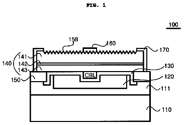
FIG. 1 is a schematic plan view showing an example of a semiconductor light-emitting element of the present invention.
FIG. 2 is a schematic sectional view taken along lines A-A' in FIG. 1.
FIG. 3 is a schematic sectional view taken along lines B-B' in FIG. 1.
FIG. 4 is a schematic cross-sectional view showing an example of a laminated semiconductor layer of a semiconductor light-emitting element of the present invention.
FIG. 5 is an enlarged cross-sectional view of an example of a p-type electrode of the semiconductor light-emitting element of the present invention.
FIG. 6A is a cross-sectional view showing an example process of the p-type electrode of the light-emitting element of the present invention.
FIG. 6B is a cross-sectional view showing an example process of the p-type electrode of the light-emitting element of the present invention.
FIG. 6C is a cross-sectional view showing an example process of the p-type electrode of the light-emitting element of the present invention.
FIG. 6D is a cross-sectional view showing an example process of the p-type electrode of the light-emitting element of the present invention.
FIG. 7A is a cross-sectional view showing an example process of the p-type electrode of the light-emitting element of the present invention.
FIG. 7B is a cross-sectional view showing an example process of the p-type electrode of the light-emitting element of the present invention.
FIG. 7C is a cross-sectional view showing an example process of the p-type electrode of the light-emitting element of the present invention.
FIG. 8A is a cross-sectional view showing an example process of the p-type electrode of the light-emitting element of the present invention.
FIG. 8B is a cross-sectional view showing an example process of the p-type electrode of the light-emitting element of the present invention.
FIG. 8C is a cross-sectional view showing an example process of the p-type electrode of the light-emitting element of the present invention.
FIG. 8D is a cross-sectional view showing an example process of the p-type electrode of the light-emitting element of the present invention.
FIG. 9A is a cross-sectional view showing an example process of the p-type electrode of the light-emitting element of the present invention.
FIG. 9B is a cross-sectional view showing an example process of the p-type electrode of the light-emitting element of the present invention.
FIG. 9C is a cross-sectional view showing an example process of the p-type electrode of the light-emitting element of the present invention.
FIG. 9D is a cross-sectional view showing an example process of the p-type electrode of the light-emitting element of the present invention.
FIG. 10 is a schematic cross-sectional view showing an example of a lamp of the present invention.
FIG. 11 is a schematic cross-sectional view showing an example of the semiconductor light-emitting element of the present invention.
Best mode for carrying out the invention
Preferred embodiments for carrying out the present invention will be described below. However, the present invention is not limited to the following examples, and modifications, additions and omissions may be made as needed in the number, position, material, shape and the like, unless otherwise specifically limited.
(First Embodiment)
FIGS. 1 to 5 show an example of a semiconductor light-emitting element, which is an embodiment of the present invention. FIG. 1 is a schematic plan view of the semiconductor light-emitting element, which is the embodiment of the present invention, FIG. 2 is a schematic cross-sectional view taken along lines A-A' in FIG. 1, FIG. 3 is a schematic cross-sectional view taken along lines B-B' in FIG. 1, FIG. 4 is a schematic cross-sectional view of a laminated semiconductor layer which constitutes the semiconductor light-emitting element shown in FIG. 1, and FIG. 5 is an enlarged cross-sectional view of a p-type electrode of the semiconductor light-emitting element shown in FIG. 1.
(Semiconductor Light Emitting Element)
As shown in FIG. 1, a semiconductor light-emitting element 1 has a rectangular shape in a plan view. One side thereof is cut away in a half-circular and half-rectangular shape, so that a cutout 16 and a cutout body 17 are defined.
An n-type electrode 108 having an approximately circular shape in a plan view is provided in the cutout 16. The side wall of the n-type electrode 108 and the surroundings thereof are covered with a protective film 10.
The cutout body 17 of the semiconductor light-emitting element 1 is also covered with the protective film 10. A bonding layer 55 is exposed in a concave (recess) 111c which has a circular shape in a plan view and is provided in a part of the protective layer 10. Under the protective film 10 of the cutout body 17, an ohmic contact layer 51, a metal reflection layer 52, a first anti-diffusion layer 53, a first adhesion layer 54, a bonding layer 55 and a second adhesion layer 56 are placed in this order from the bottom in the almost same shape as the cutout body 17, of which a p-type electrode 111 is composed.
As shown in FIGS. 2 and 3, the semiconductor light-emitting element 1 of the present invention extracts light in the direction fat the side of a substrate 101. A buffer layer 102, a base layer 103 and a laminated semiconductor layer 20 are sequentially laminated on the substrate 101. The p-type electrode 111 is formed on the laminated semiconductor layer 20 at a face (hereinafter, top face) 106c opposite to the face where the substrate 101 is provided. The n-type electrode 108 is formed on an exposed face 104c of the n-type semiconductor layer 104, which is formed by cutting away a part of the laminated semiconductor layer 20. The foregoing is a general constitution of the semiconductor light-emitting element 1. The laminated semiconductor layer 20 is constituted by the n-type semiconductor layer 104, a light-emitting layer 105 and the p-type semiconductor layer 106 which are laminated in this order from the side of the substrate 101.
The p-type electrode 111 is constituted by the ohmic contact layer 51, metal reflection layer 52, first anti-diffusion layer 53, first adhesion layer 54, bonding layer 55, second adhesion layer 56 and protective film 10 which are laminated in this order on the top face 106c of the p-type semiconductor layer 106.
The protective layer 10 covers the semiconductor layer exposed face 104c and the side face of the n-type electrode 108 as well as the top and side faces of the p-type semiconductor layer 106.
The respective members will be described below.
<Substrate>
The substrate 101 is not limited specifically, and any substrate may be employed, as long as it is transparent and a group III nitride semiconductor crystal can be grown epitaxially on its surface. For example, there can be used substrates of sapphire, zinc oxide, magnesium oxide, zirconium oxide, magnesium aluminum oxide, gallium oxide, indium oxide, lithium gallium oxide, lithium aluminum oxide, neodymium gallium oxide, lanthanum strontium aluminum tantalum oxide, strontium titanium oxide, titanium oxide, hafnium, tungsten, molybdenum and the like.
In particular, a sapphire substrate having a main face of c-plane is preferably employed, and it is preferable to form the buffer layer 102 on the c-plane of sapphire.
<Laminated Semiconductor Layer>
A laminated semiconductor layer 20 is selected as necessary. For example, preferable is a layer of a group III nitride semiconductor in which the n-type semiconductor layer 104, light-emitting layer 105 and p-type semiconductor layer 106 are laminated on the substrate 101 in this order as shown in FIGS. 2 and 3. The laminated semiconductor layer 20 may further include the base layer 103 and buffer layer 102.
As shown in FIG. 4, the n-type semiconductor layer 104, light-emitting layer 105 and p-type semiconductor layer 106 may be each composed of a plurality of semiconductor layers.
The laminated semiconductor layer 20 having fine crystallinity can be obtained by an MOCVD method. Even by sputtering, however, a semiconductor layer having better crystallinity than by an MOCVD can be formed under optimized conditions. They will be described below individually.
<Buffer Layer>
The buffer layer 102 is selected as needed. It is preferably made of polycrystalline Al.sub.xGa.sub.1-xN (0.ltoreq.x.ltoreq.1), and more preferably single-crystalline Al.sub.xGa.sub.1-xN (0.ltoreq.x.ltoreq.1).
For example, the buffer layer 102 may be a layer of polycrystalline Al.sub.xGa.sub.1-xN (0.ltoreq.x.ltoreq.1) having a thickness of 0.01 .mu.m to 0.5 .mu.m as described above. When the buffer layer 102 has a thickness of less than 0.01 .mu.m, the buffer layer 102 may not have a sufficient effect of mitigating a difference in lattice constant between the substrate 101 and base layer 103. When the buffer layer 102 has a thickness of more than 0.5 .mu.m, a film deposition process of the buffer layer 102 takes a longer time, which may result in lower productivity despite no change in the function of the buffer layer 102.
The buffer layer 102 has the functions of mitigating a difference in lattice constant between the substrate 101 and base layer 103 and making it easier to form a c axis-oriented monocrystalline layer on the
c-plane of the substrate 101. Therefore it is possible to laminate the base layer 103 having even better crystallinity, when the base layer 103 of single crystal is laminated on the buffer layer 102. In the present invention, it is preferable to carry out a buffer layer forming step, although it is not necessary.
The buffer layer 102 may have a hexagonal crystal structure of a group III nitride semiconductor. The crystal of the group III nitride semiconductor of the buffer layer 102 may or may not have a single crystal structure, and one having a single crystal structure is preferably used. By controlling growth conditions, the crystal of the group III nitride semiconductor grows not only in the upward direction but also in the in-plane direction, so as to form a single crystal structure. Therefore it is possible to form the buffer layer 102 made of a single crystal group III nitride semiconductor by controlling its deposition conditions. When the buffer layer 102 having such a single crystal structure is deposited on the substrate 101, the buffer layer 102 exerts the buffering function effectively. The group III nitride semiconductor deposited thereon thus becomes a crystal film having satisfactory orientation and crystallinity.
It is also possible to make the group III nitride semiconductor constituting the buffer layer 102 to be a columnar crystal having an aggregate structure mainly composed of hexagonal columns (polycrystal) by controlling the deposition conditions. The "columnar crystal having an aggregate structure" means a crystal in which adjacent crystal grains are separated from each other by a grain boundary formed therebetween, and each grain has a columnar shape in cross-section.
<Base Layer>
The base layer 103 is selected as needed. Al.sub.xGa.sub.yIn.sub.zN (0.ltoreq.x.ltoreq.1, 0.ltoreq.y.ltoreq.1, 0.ltoreq.z.ltoreq.1, x+y+z=1) can be given as an example, and it is preferable to employ Al.sub.xGa.sub.1-xN (0.ltoreq.x.ltoreq.1) since it can form the base layer 103 having satisfactory crystallinity.
The base layer 103 has a film thickness of preferably 0.1 .mu.m or more, more preferably 0.5 .mu.m or more, and most preferably 1 .mu.m or more. The film thicknesses as above make it easier to obtain an Al.sub.xGa.sub.1-xN layer having satisfactory crystallinity. The upper limit may not be specifically defined, but for example, it is preferably 6 .mu.m or less.
It is preferable not to dope an impurity to the base layer 103 in order to improve the crystallinity of the base layer 103. However, if p- or n-type conductivity is required, it is possible to dope an acceptor or donor impurity.
<N-Type Semiconductor>
The n-type semiconductor layer 104, which is included in the laminated semiconductor layer, is selected as needed. As shown in FIG. 4, it is generally preferable that it be composed of an n-contact layer 104a and an n-clad layer 104b. It is also possible for the n-contact layer 104a to double as the n-clad layer 104b. Also, the n-type semiconductor layer 104 includes the above base layer.
The n-contact layer 104a is for installing the n-type electrode. The n-contact layer 104a is preferably composed of an Al.sub.xGa.sub.1-xN layer (0.ltoreq.x<1, preferably 0.ltoreq.x.ltoreq.0.5, and more preferably 0.ltoreq.x.ltoreq.0.1).
It is preferable that the n-contact layer 104a be doped with an n-type impurity. From the viewpoint of retaining satisfactory ohmic contact with the n-type electrode, it is preferable to contain the n-type impurity at a concentration of 1.times.10.sup.17 to 1.times.10.sup.20/cm.sup.3, preferably 1.times.10.sup.18 to 1.times.10.sup.19/cm.sup.3. There is no particular limitation on the n-type impurity, and examples of the n-type impurity include Si, Ge, Sn and the like. Si and Ge are preferable.
The n-contact layer 104a has a film thickness of preferably 0.5 to 5 .mu.m, and more preferably in the range of 1 to 3 .mu.m. When the n-contact layer 104a has a film thickness within the above range, satisfactory crystallinity of the semiconductor is maintained.
It is preferable that the n-clad layer 104b be provided between the n-contact layer 104a and light-emitting layer 105. The n-clad layer 104b is provided to inject and confine carriers in the light-emitting element 105. The n-clad layer 104b can be formed with AlGaN, GaN, GaInN or the like. It is also possible to join these structures with each other by a hetero-junction, or to laminate them plural times to form a super-lattice structure. When the n-clad layer 104b is formed with GaInN, it goes without saying that the band gap thereof is desirably made larger than that of GaInN of the light-emitting layer 105.
There is no particular limitation on the film thickness of the n-clad layer 104b, and the film thickness is preferably 0.005 .mu.m to 0.5 .mu.m, and more preferably 0.005 .mu.m to 0.1 .mu.m. The n-clad layer 104b has an n-type doping concentration of preferably 1.times.10.sup.17 to 1.times.10.sup.20/cm.sup.3, and more preferably 1.times.10.sup.18 to 1.times.10.sup.19/cm.sup.3. It is preferable that the doping concentration be within the above range from the viewpoint of retaining satisfactory crystallinity and reducing working voltage of the element.
Although not shown in detail, when the n-clad layer 104b has a super-lattice structure, it may have a laminated structure of an n-side first layer of a group III nitride semiconductor having a film thickness of 100 .ANG. or less and an n-side second layer also of a group III nitride semiconductor having a film thickness of 100 .ANG. or less but having a different composition from the n-side first layer.
Also, the n-clad layer 104b may have a repeatedly laminated structure of the alternating n-side first and second layers. Preferably, one of the n-side first and second layers is in contact with the active layer (light-emitting layer 105).
<Light Emitting Layer>
The light-emitting layer 105, which is laminated on the n-type semiconductor layer 104, is selected as needed. For example, the light-emitting layer 105 has a single quantum well structure, multiple quantum well structure, or the like.
A group III nitride semiconductor layer of Ga.sub.1-yIn.sub.yN (0<y<0.4) is generally employed as a well layer 105b of a quantum well structure as shown in FIG. 4. The well layer 105b may have a film thickness with which a quantum effect is achieved, for example, 1 nm to 10 nm. Preferably, it is 2 nm to 6 nm from the viewpoint of light output.
When the light-emitting layer 105 has a multiple quantum well structure, the above Ga.sub.1-yIn.sub.yN is used as the well layer 105b and Al.sub.zGa.sub.1-zN (0.ltoreq.z<0.3), which has larger bandgap energy than the well layer 105b, is used as a barrier layer 105a. The well layer 105b and barrier layer 105a may not be doped with impurity depending on the design.
<P-Type Semiconductor Layer>
The description continues in the full USPTO document.
 Lapsed, fee not paid16 drawings