Cross-reference to related application
This application claims priority to Japanese Patent Application No. 2009-249504, which was filed on Oct. 29, 2009, the content of which is incorporated herein by reference in its entirety.
Background of the invention
1. Field of the invention
The present invention relates to a charging device of corona discharge type, an image forming apparatus comprising the charging device, and a method for forming a discharge electrode.
2. Description of the related art
Heretofore, in an image forming apparatus which employs an electrophotographic system, a charging device of corona discharge type (corona discharge device) has commonly been used for a charging device for charging a photoreceptor, a transfer device for effecting electrostatic transfer printing of a toner image to a recording paper sheet, a separating device for effecting electrostatic separation of a recording sheet, and so forth.
As a corona discharge device, there is known a corona discharge device of so-called corotron type, which comprises a shield case having an opening formed to face an object to be charged such as a photoreceptor or a recording paper sheet, and a discharge electrode disposed in the interior space of the shield case. In the corotron-type corona discharge device, upon application of a high voltage, corona discharge takes place at the discharge electrode. A stream of ions generated through the corona discharge travels toward an object to be charged so as to generate a discharge current, with the consequence that an object to be charged is brought into a charged state.
As another corona discharge device, there is known a corona discharge device of so-called scorotron type, which is constructed by adding a grid electrode to the structure of the corotron-type corona discharge device. The grid electrode is disposed between a discharge electrode and an object to be charged. In the scorotron-type corona discharge device, a voltage of predetermined level is applied to the grid electrode at the time of corona discharge, so that an object to be charged can be charged even more uniformly. However, in the corona discharge devices of corotron type and scorotron type, there is a need to pass a large quantity of discharge current to bring electric discharge into a condition of stability, which gives rise to the problem of generation of large amounts of ozone.
As a charging device other than the corona discharge device, there is known a contact-type charging device having a charging member formed of a semiconducting roller or brush. In this construction, the charging member is brought into contact with or placed proximately to face an object to be charged, and a voltage is applied between the charging member and the object to be charged, so that the object to be charged can be charged. According to the contact-type charging device, the region of electric discharge is limited to a minute gap created in the vicinity of the part of contact between an object to be charged and the charging member. Therefore, in the contact-type charging device, in contrast to the corona discharge device, the amount of discharge current can be reduced. Accordingly, the contact-type charging device is capable of reduction in the amount of ozone generation.
However, the contact-type charging device poses the following problems. The charging member is prone to abrasion and quality degradation due to the contact with an object to be charged, electrical stress, and so forth, which makes it difficult to achieve speeding-up of a charging process, as well as to impart a long operable life to the charging member. Furthermore, the charging characteristics of the contact-type charging device are likely to deteriorate due to changes in the properties of the charging member ascribable to contamination, environmental conditions, a lapse of time, and so forth.
In addition to that, a technology to achieve superimposition of multi-color images on a photoreceptor (called IOI: Image On Image) has been developed in recent times. The IOI technology affords the advantages of being less prone to displacements of images of a plurality of colors and of causing little image quality deterioration because of just one time of a transfer process being required, and is therefore excellent in production of high-quality images. However, the IOI technology is not adapted to the use of a contact-type charging device. Accordingly, the IOI technology necessitates a non-contact type charging device which exhibits high charging uniformity.
In view of such circumstances, in the design of corona discharge devices of corotron type, scorotron type, etc. attempts have been made to achieve a reduction in the amount of ozone generation, an increase in longevity, improvement in charging characteristics, and so forth.
In Japanese Unexamined Patent Publication JP-A 6-11946 (1994), there is disclosed a charging device built as a corona discharge device having a discharge electrode of serrated configuration. In the corona discharge device having, like the discharge electrode of serrated configuration, a discharge electrode having sharp-pointed projections, an electric field tends to be concentrated on the projections, and also the number of electric discharge points is reduced. Accordingly, even if the level of a voltage to be applied is relatively low, it is possible to effect corona discharge, wherefore generation of ozone can be suppressed.
However, in the corona discharge device equipped with a discharge electrode having projections, variations in the state of electric discharge are caused by abrasion of the projections, adhesion of discharge products, and so forth. This leads to unevenness in the charged potential of an object to be charged in the direction of the length of the corona discharge device, with the consequent possibility that the charging uniformity of an object to be charged will be impaired. In the event of, for example, abrasion of the projections, in order to prevent impairment of the charging uniformity, as a condition for voltage application, the level of a voltage to be applied is set to be higher than normal so that required discharge current can be generated even at the projection in a state where electric discharge is less likely to occur. However, an increase in the level of an applied voltage results in excessive electric discharge at the projection in a state where electric discharge occurs readily. This leads to occurrence of unnecessary electric discharge that does not contribute to charging of an object to be charged, with a consequent undesirable increase in the amount of ozone generation.
As a technique to overcome such a problem, in Japanese Unexamined Patent Publications JP-A 5-2314
and JP-A 8-160711 (1996), there is disclosed a technology to divide a discharge electrode of serrated configuration into pieces on a projection-by-projection basis so as to connect an electric resistor element between each of the projections and a power source. In such a structure, in the projection where the amount of discharge current is large, a drop in voltage caused by the connected electric resistor element is significant, and the applied voltage is decreased correspondingly, wherefore corona discharge is restricted. On the other hand, in the projection where the amount of discharge current is small, a drop in voltage caused by the connected electric resistor element is insignificant, and the applied voltage is increased correspondingly, wherefore corona discharge is accelerated. Thus, according to the technology presented in JP-A 5-2314 and JP-A 8-160711, variations in a stream of ions among the projections can be reduced, with the consequent improvement in charging uniformity. Moreover, since satisfactory charging uniformity can be attained even if the applied voltage is decreased to reduce the total amount of discharge current, it is possible to reduce the amount of ozone generation. It is noted that, however, the manufacturing cost will be increased because of the necessity for providing an electric resistor element in the corona discharge device.
In Japanese Unexamined Patent Publication JP-A 7-104549 (1995), there is disclosed a technology to achieve improvement in charging uniformity in a scorotron-type discharge device by reducing the aperture ratio of a grid electrode opposed to a tip end portion of a discharge electrode, viz., a discharge region, so that part of a stream of ions can be absorbed by the grid electrode. According to the technology presented in JP-A 7-104549, improvement in charging uniformity can be achieved in a simple manner with low cost. However, the negative side is that, as a stream of ions traveling toward an object to be charged is absorbed by the grid electrode, there will be a drop in the charged potential of an object to be charged correspondingly.
In Japanese Unexamined Patent Publication JP-A 11-212335 (1999), there is disclosed a charging device comprising an electric field regulation member to eliminate a ripple in charged potential, as will hereinafter be described. A paragraph
of JP-A 11-212335 states that the pitch of projections of a discharge electrode should preferably be increased to achieve reduction in the amount of ozone generation and improvement in the charging uniformity of an object to be charged as well. In order to verify this suggestion, an electric discharge test was performed on each of a case under a condition where the pitch of projections of a discharge electrode is narrow and a case under a condition where the pitch of the projections thereof is wide. The measurement of a charged potential at an object to be charged has been carried out by means of an experiment system as shown in FIG. 2 that will hereinafter be described. In a corona discharge device having no grid electrode (corotron), discharge electrodes of varying projection pitch were mounted individually. Upon charging a photoreceptor, a charged potential on the surface of the photoreceptor was measured in a direction along the length of the photoreceptor.
FIGS. 8A to 8D are views showing a relationship between a projection pitch in a discharge electrode and charging uniformity. As to the condition where the projection pitch of a discharge electrode A1 is narrow as shown in FIG. 8A, as shown in FIG. 8B, irregular fluctuations were observed in the charged potential of the photoreceptor. Furthermore, as the result of observation of the projections of the discharge electrode A1 under this condition, as shown in FIG. 8A, it has been found that, among the projections, some undergo light emission A2 resulting from electric discharge, but others don't, with consequent lack of uniformity in the state of electric discharge. Thus, when the state of electric discharge is not uniform, although it is possible to attain at least practically acceptable charging uniformity by, as has already been described, increasing discharge current or by providing a narrow grid electrode as presented in JP-A 8-160711, unnecessary electric discharge has to be conducted. This leads to an increase in the amount of ozone generation as is undesirable.
On the other hand, as to the condition where the projection pitch of the discharge electrode A1 is wide as shown in FIG. 8C, as shown in FIG. 8D, a ripple took place in the charged potential. However, this is not irregular fluctuations but regular periodic fluctuations that occur at intervals substantially equivalent to the pitch distance between the projections. Moreover, as the result of observation of the state of light emission during electric discharge, as shown in FIG. 8C, it has been found that each and every projection undergoes light emission A2 resulting from electric discharge and that electric discharge takes place at each and every projection in a relatively stable condition. Further, a comparison was made between the case under the condition where the pitch is narrow and the case under the condition where the pitch is wide in respect of the amount of ozone generation. At this time, the amount of discharge current for the former case and that for the latter case were set at the same value. The result is that the case under the condition where the pitch is wide yielded a reduction in the amount of ozone generation. It is noted that, however, it was found to be difficult to eliminate the ripple occurring in the charged potential under the condition where the pitch is wide in spite of the provision of a grid electrode.
In this regard, according to the JP-A 11-212335, with the provision of an electric field regulation member between a tip end portion of the discharge electrode and another tip end portion adjacent thereto, a stream of ions coming from the projection can be deflected in the direction of the length of an object to be charged. This makes it possible to achieve improvement in charging uniformity, and further achieve both reduction in the amount of ozone generation and improvement in charging uniformity at one time.
However, even if the charging device presented in JP-A 11-212335 is adopted for use, there still remains unevenness in charged potential. This problem will be described hereinbelow.
At first, an electric discharge test was conducted with use of a conventional corona discharge device. FIGS. 9A to 9C are views showing how electric discharge is to be effected in the conventional corona discharge device. The conventional corona discharge device is a scorotron-type corona discharge device having stylus electrodes H arranged at regular intervals. Instead of a grid electrode, a counter electrode T for permitting arrival of a stream of ions generated is disposed at a location spaced a predetermined distance away from the tip end of the stylus electrode H. With this construction, an electric discharge test was conducted. At that point in time when dozens of hours have elapsed since the start of the electric discharge test, as shown in FIG. 9B, elliptical traces of demarcations of ion streams were observed on a surface of the counter electrode T. As will be understood from the demarcation traces of ion streams, as shown in FIG. 9A, a stream of ions is readily diffused in a direction perpendicular to the direction of arrangement of the stylus electrodes H. However, as shown in FIG. 9C, in the direction of arrangement of the stylus electrodes H, ion streams generated from the adjacent stylus electrodes H, respectively, are repelled by each other and are thus less likely to diffuse uniformly.
It has thus been found that, in the conventional corona discharge device such as presented in JP-A 6-11946, even in the absence of abrasion of the projections, adhesion of discharge products, and the like problem, the charged potential of an object to be charged is caused to drop at a position thereof opposed to a point midway between the adjacent projections due to the repulsion of ion streams, with a consequent deterioration in the charging uniformity of an object to be charged. It has also been found that, even in the case of designing the apparatus so that electric discharge occurs at all of the projections by setting the projection pitch to be relatively wide or by inserting an electric resistor element as in the charging device presented in JP-A 5-2314 and JP-A 8-160711, the charged potential of an object to be charged is caused to drop at a position thereof opposed to a point midway between the adjacent projections, and that the drop of the charged potential of an object to be charged becomes increasingly significant as the pitch of the projections is increased.
Next, for verification of the inability of the charging device presented in JP-A 11-212335 to resolve the above-described problem of a drop in the charged potential of an object to be charged, an electric discharge test was conducted with use of a charging device 57 as shown in FIG. 10 that is identical in structure with said charging device. FIG. 10 is a schematic diagram showing the charging device 57 as viewed from a surface of an object to be charged. The charging device 57 comprises a plurality of projections 55 and electric field regulation members 54. The electric field regulation members 54 are arranged symmetrically with respect to a straight line Z which passes through the tip end of the projection 55 and is thus perpendicular to the direction of arrangement of the projections 55.
In the charging device 57, the electric field regulation member 54 caused a stream of ions 56 generated from the projection 55 to spread all around so as to be deflected in substantially square form. In this way, the stream of ions 56 generated from the projection 55 diffused in a wider area than does a stream of ions spreading in elliptical form.
However, the streams of ions 56 generated from the adjacent projections 55, respectively, were repelled by each other, and consequently the extent of diffusion in the direction of the length of the charging device 57 was lesser than in the case where no electric field regulation member 54 is provided. Therefore, upon moving an object to be charged relative to the direction of the width of the charging device 57, then the object to be charged was inconveniently moved relatively along the demarcations of the streams of ions 56, in consequence whereof there resulted a drop of a charged potential in streak form on the object to be charged. This gave rise to deterioration in the charging uniformity of the object to be charged.
FIG. 11 is a graph showing a distribution of charged potentials at an object to be charged in the case of using the charging device 57. It will be understood from the graph that, upon charging an object to be charged by the charging device 57, in contrast to a position P1, a position P2, a position P3, a position P4, a position P5, a position P6, and a position P7 on the object to be charged that are opposed to their respective projections 55, at positions on the object to be charged near a midway point M1 between P1 and P2, a midway point M2 between P2 and P3, a midway point M3 between P3 and P4, a midway point M4 between P4 and P5, a midway point M5 between P5 and P6, and a midway point M6 between P6 and P7, respectively, viz., at each position thereon opposed to a point midway between the adjacent projections, a drop in the charged potential occurs. It has thus been found that there is still lack of uniformity in charging on an object to be charged even in the case of using the charging device 57 comprising the electric field regulation member 54.
Summary of the invention
The invention has been devised in order to solve the foregoing problems, and accordingly its object is to provide a charging device capable of improvement in charging uniformity on an object to be charged, as well as an image forming apparatus comprising the charging device, and a method for forming a discharge electrode.
The invention provides a charging device comprising:
a shield case having an opening; and
a discharge electrode disposed in an interior space of the shield case, having a plurality of projections aligned in one direction from which a stream of ions is generated, the plurality of projections each being so disposed that a width direction thereof makes a predetermined angle with a direction of arrangement of the plurality of projections, in order that streams of ions generated from the projections that are adjacent to each other in a lengthwise direction of the shield case can overlap each other when viewed in a widthwise direction of the shield case.
According to the invention, the projections of the discharge electrode each are disposed inclined so that a width direction thereof makes a predetermined angle with a direction of arrangement of the projections. Accordingly, a stream of ions generated from each of the projections is deflected obliquely with respect to the direction of arrangement of the projections. Correspondingly, an ion-stream demarcated portion (a portion with decreased ion stream density) resulting from the repulsion of the ion streams generated from the adjacent projections, respectively, are also deflected obliquely. Therefore, when an object to be charged is moved relative to the widthwise direction of the shield case, it never occurs that the direction of movement of an object to be charged and the portion with decreased ion stream density come into line with each other. Hence, even if an object to be charged is moved relative to the widthwise direction of the shield case, the ion stream density on an object to be charged will never become nonuniform. Accordingly, the charging device pursuant to the invention is capable of improving the charging uniformity of an object to be charged.
Moreover, in the invention, it is preferable that the discharge electrode is so constituted that the projections are inclined in the same direction and a condition of p<W/{2 tan(.alpha.)}+W/{2 tan(.beta.)} is fulfilled,
wherein W denotes a width of the shield case, .alpha. and .beta. denote predetermined angles of given two projections arranged adjacent to each other in a lengthwise direction of the shield case, respectively, and p denotes a pitch of tip ends of the two projections.
According to the invention, the discharge electrode is so constituted that the projections are inclined in the same direction and the condition of p<W/{2 tan(.alpha.)}+W/{2 tan(.beta.)} is fulfilled. This makes it possible to adjust a stream of ions to deflect in an optimum condition and thereby construct a charging device which is excellent in charging uniformity.
Moreover, in the invention, it is preferable that the discharge electrode is so constituted that predetermined angles of all of the projections of the discharge electrode are the same.
According to the invention, the discharge electrode is so constituted that all of the projections thereof are at the same angle in the widthwise direction with respect to the direction of arrangement of the projections. This makes it possible to suppress the repulsion of ion streams generated from the projections and thereby improve the charging uniformity of an object to be charged even further in the direction of arrangement of the projections.
Moreover, in the invention, it is preferable that the charging device further comprises a holding portion for retaining the discharge electrode in the interior space of the shield case,
the discharge electrode is constructed by bending a plate-like material, and
the holding portion serves as a bending member which is used to form the discharge electrode by bending the plate-like material.
According to the invention, the discharge electrode can be retained in a bent state by the holding portion. This makes it possible to keep the angle of the projection in the widthwise direction with respect to the direction of arrangement of the projections with high accuracy, and thereby maintain the charging uniformity of an object to be charged in the direction of arrangement of the projections.
The invention also provides an image forming apparatus comprising:
an image bearing member for bearing an electrostatic latent image thereon; and
the charging device mentioned above,
the image bearing member being charged by the charging device.
According to the invention, since the image bearing member is charged by the charging device pursuant to the invention, it is possible to form high-quality images. Moreover, the image forming apparatus pursuant to the invention is capable of a reduction in the amount of ozone generation entailed by charging operation. Further, since the charging device pursuant to the invention achieves improvement in charging uniformity with a simple structure, it is possible to make the image forming apparatus compact in size at low cost.
The invention further provides a discharge electrode forming method for forming a discharge electrode which is provided in the charging device mentioned above by bending a single plate-like material.
According to the invention, the discharge electrode is formed simply by bending a single plate-like material. This makes it possible to achieve formation of the discharge electrode with ease and at low cost.
Moreover, in the invention, it is preferable that the plate-like material is bent in such a manner that widthwise one end of the respective projections of the discharge electrode is separated from the plate-like material, whereas widthwise the other end thereof is kept connected with the plate-like material.
According to the invention, the discharge electrode is formed by bending the plate-like material in such a manner that widthwise one end of the respective projections is separated from the plate-like material, whereas widthwise the other end thereof is kept connected with the plate-like material. This helps reduce the amount of the plate-like material to be used.
Brief description of the drawings
Other and further objects, features, and advantages of the invention will be more explicit from the following detailed description taken with reference to the drawings wherein:
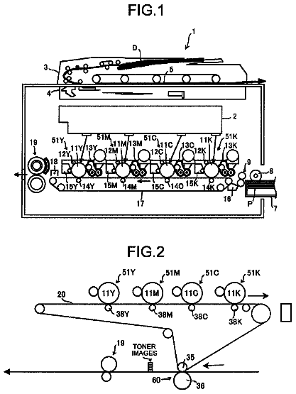
FIG. 1 is a diagram schematically showing a cross-section of an image forming apparatus;
FIG. 2 is a view schematically showing an outer appearance of a charging device and a photoreceptor drum;
FIGS. 3A to 3C are views showing the structure of the charging device;
FIGS. 4A to 4C are views for explaining a method of forming a discharge electrode;
FIGS. 5A to 5C are views showing a state of a stream of ions generated from a projection;
FIGS. 6A to 6C are views for explaining the effect of obliquely deflected ion streams to improve charging uniformity of an object to be charged;
FIGS. 7A to 7C are views for explaining a discharge electrode;
FIGS. 8A to 8D are views showing a relationship between a projection pitch in a discharge electrode and charging uniformity
FIGS. 9A to 9C are views showing how electric discharge is to be effected in a conventional corona discharge device;
FIG. 10 is a schematic diagram showing the charging device as viewed from a surface of an object to be charged; and
FIG. 11 is a graph showing a distribution of charged potentials at an object to be charged in the case of using the charging device.
Detailed description
Now referring to the drawings, preferred embodiments of the invention will be described in detail.
An image forming apparatus 1 which is an embodiment of the image forming apparatus pursuant to the invention comprises an image bearing member and a charging device 12 which is a first embodiment of the charging device pursuant to the invention. FIG. 1 is a diagram schematically showing a cross-section of the image forming apparatus 1. The image forming apparatus 1 is built as an electrophotographic image forming apparatus of tandem design for forming images by overlaying toner images of four colors: yellow (y); magenta (m); cyan (c); and black (b) on top of one another to form a multi-color toner image and then fixing the multi-color toner image onto a recoding medium. The image forming apparatus 1 includes a toner image forming section 2, an intermediate transfer section 3, a secondarily transfer section 4, a recording medium supply section 5, a fixing section 6, a scanner section 7, and a control unit section (not shown).
The scanner section 7 includes an original platen, a light source, and a CCD (Charge Coupled Device) image sensor 9. On the top surface of the original platen is placed a source document to be copied. The original platen is constructed of a plate-like member made of a transparent material such as transparent glass. The light source illuminates the source document placed on the original platen. The CCD image sensor 9 performs photoelectric conversion on light reflected from the source document illuminated by the light source thereby to convert the reflected light into image information (analog signal).
The CCD image sensor 9 includes a conversion portion, a transmission portion, and an output portion. The conversion portion converts an optical signal, which is reflected light, into an electrical signal. The transmission portion transmits electrical signals one after another to the output portion in synchronization with clock pulses. The output portion converts an electrical signal into a voltage signal, amplifies the voltage signal, and puts it out with a decrease in impedance.
The control unit section, which controls overall workings of the image forming apparatus 1, includes a control portion, a calculation portion, and a memory portion as will hereinafter be described, for converting an analog signal thereby obtained into a digital signal through heretofore known image processing. The image information of the source document read out by the scanner section 7 is sent to the control unit section where it is converted into a digital signal through various image processing steps, and is whereafter stored in the memory portion of the control unit section. The image information stored in the memory portion is retrieved from the memory portion in response to an output instruction, and is then transmitted to an optical scanning unit 13 which will hereinafter be described.
According to the scanner section 7, the source document placed on the original platen is illuminated by the light source, and the light reflected from the illuminated source document is converted into analog image information by the CCD image sensor 9. The image information is changed from analog signal form to digital signal form by the control unit section, and the digital image information is stored in the memory portion.
The toner image forming section 2 includes visible image forming units 10y, 10m, 10c, and 10b, and the optical scanning unit 13. The visible image forming units 10y, 10m, 10c, and 10b are arranged side by side, in the order named, from the upstream side in a direction in which a subsequently-described intermediate transfer belt 21 is driven to turn; that is, in a direction indicated by an arrow 27. The visible image forming units 10y, 10m, 10c, and 10b form electrostatic latent images corresponding to image information of their respective colors inputted as digital signals, and then supply toner to the electrostatic latent images thereby to form toner images of their respective colors.
The visible image forming unit 10y forms a toner image corresponding to yellow (y) image information. The visible image forming unit 10m forms a toner image corresponding to magenta (m) image information. The visible image forming unit 10c forms a toner image corresponding to cyan (c) image information. The visible image forming unit 10b forms a toner image corresponding to black (b) image information. As to the visible image forming units 10y, 10m, 10c, and 10b that are provided to deal with different colors, collectively, they are designated only by the general reference numeral 10. On the other hand, when it is desired to make distinctions among the visible image forming units 10y, 10m, 10c, and 10b according to their colors, they are designated by the reference numeral 10 with the alphabetical suffix indicative of specific color. The above conditions hold true for the individual components constituting the visible image forming unit 10.
The visible image forming unit 10 includes a photoreceptor drum 11, a charging device 12, a developing portion 14, a drum cleaner 15, a pre-primary transfer charging portion 16, a primary transfer portion 22, and a photoreceptor charge eliminating portion 33.
The photoreceptor drum 11 is constructed of a roller-shaped member which is so supported as to be driven to rotate about its axis by a non-illustrated driving portion. The photoreceptor drum 11 includes a photosensitive layer and serves as an image bearing member for bearing, on the surface of the photosensitive layer, an electrostatic latent image and thus a toner image.
As exemplary of the photoreceptor drum 11, a component composed of a conductive substrate made of aluminum or the like and a photosensitive layer formed on a surface of the conductive substrate can be used. As exemplary of the conductive substrate, a cylindrical conductive substrate, a columnar conductive substrate, and a sheet-shaped conductive substrate can be used. Among them, the use of a cylindrical conductive substrate is particularly desirable. Exemplary of the photosensitive layer are an organic photosensitive layer and an inorganic photosensitive layer.
Examples of the organic photosensitive layer include a laminated body including a charge generating layer which is a charge generating substance-containing resin layer and a charge transporting layer which is a charge transporting substance-containing resin layer; and a single resin layer containing both a charge generating substance and a charge transporting substance. Examples of the inorganic photosensitive layer include a resin layer containing one or two or more of substances selected among from zinc oxide, selenium, amorphous silicon, and so forth.
It is possible to interpose an undercoat layer between the conductive base body and the photosensitive layer, as well as to provide a surface layer (protective layer) on the surface of the photosensitive layer for its protection.
FIG. 2 is a view schematically showing the outer appearance of the charging device 12 and the photoreceptor drum 11. The charging device 12 is disposed to face the photoreceptor drum 11 so as to extend along a lengthwise direction 44 of the photoreceptor drum 11. The charging device 12 comprises a discharge element 35 and a shield case 34. Also provided in the charging device 12 are a surface potential indicator 45 and a surface potential probe 46 for measuring the surface potential of the photoreceptor drum 11. It is noted that, in an embodiment of the charging device 12, the surface potential probe 46 and the surface potential indicator 45 do not necessarily have to be provided.
The discharge element 35 comprises a discharge electrode which is an electrode to be connected with a high voltage power source 47. The discharge electrode has a plurality of projections. In the discharge electrode, upon application of a voltage thereto by the high voltage power source 47, corona discharge takes place in at least one of the projections.
Although a voltage applied by the high voltage power source 47 varies in polarity depending upon which one of opposite polarities is to be selected for the charging of an object to be charged, the absolute value of an applied voltage is so adjusted as to fall in the range from 4 kV to 10 kV. Moreover, although a required applied voltage varies depending upon the distance between the discharge element 35 and another constituent member of the charging device 12, from a transformer cost standpoint, as well as from a safety standpoint, the maximum value (absolute value) of the applied voltage should preferably be set at or below 10 kV.
The shield case 34 is a box-shaped member having an opening formed in a wall portion thereof facing the photoreceptor drum 11. The shield case 34 has an interior space in which the discharge element 35 is disposed. The shield case 34 is so disposed that its lengthwise direction coincides with the lengthwise direction 44 of the photoreceptor drum 11. The shield case 34 has a substantially C-shaped cross-section when viewed in a direction perpendicular to the lengthwise direction.
The shield case 34 is connected to ground or is connected to a power source (not shown). When connected to the power source, the shield case 34 receives application of a voltage of the same polarity as the polarity of a voltage applied to the discharge electrode. The absolute value of a voltage to be applied to the shield case 34 falls in the range from 0 kV to 1 kV.
The charging device 12 of the present embodiment is built as a scorotron-type charging device having a grid electrode (not shown) which is disposed between the discharge electrode and the photoreceptor drum 11. The grid electrode is made of a thin-plate metal, and is spaced away from the projection of the discharge electrode by a distance falling in the range of from 4 mm to 12 mm. For example, the grid electrode may be spaced a distance of 7 mm away from the projection. It is noted that, by way of an embodiment of the invention, the charging device may be built as a corotron-type charging device not comprising a grid electrode.
The grid electrode has a plurality of through holes formed so as to pass therethrough in its thicknesswise direction, and is connected to a bias power supply (not shown). The grid electrode receives, from the bias power supply, application of a voltage of the same polarity as the polarity of a voltage applied to the discharge electrode. The absolute value of a voltage to be applied to the grid electrode is adjusted properly to the level required for image formation. For example, the absolute value is adjusted to a level in the range from 300 V to 1 kV.
According to the charging device 12, corona discharge takes place at the projection of the discharge electrode under application of a voltage by the high voltage power source 47. More specifically, a voltage to be applied to the discharge electrode is adjusted within the foregoing range in such a manner that the absolute value of the amount of current applied to the discharge electrode as a whole falls in the range from 200 .mu.A to 1000 .mu.A.
Regardless of a polarity at which an object to be charged is charged, a stream of ions which travels toward an object to be charged is generated by the corona discharge occurring in the charging device 12. The invention is concerned with the charging device capable of control (deflection) of a stream of ions generated from the projection of the discharge electrode, and an object to be charged can be charged at either polarity. The charging device pursuant to the invention will hereinafter be described in detail.
The optical scanning unit 13 applies beams of laser light 13y, 13m, 13c, and 13b, which correspond to image information of different colors, to the surfaces of, respectively, the photoreceptor drums 11y, 11m, 11c, and 11b in a charged state. In this way, on the surfaces of, respectively, the photoreceptor drums 11y, 11m, 11c, and 11b, there are formed electrostatic latent images corresponding to image information of their respective colors. As the optical scanning unit 13, a semiconductor laser or the like can be used.
The developing portion 14 includes a developing roller, a regulation blade, a developer tank, and a stirring roller. The developing roller is a roller-shaped member which is supported so as to be rotatable about its axis in the developer tank. The developing roller is so disposed that a part thereof extends outwardly into close proximity to the surface of the photoreceptor drum 11 from an opening formed on a surface of the developer tank that faces the photoreceptor drum 11.
The developing roller has a stationary magnetic pole (not shown) disposed therein. A developer is borne on the surface of the developing roller by the action of the stationary magnetic pole. In a location where the developing roller and the photoreceptor drum 1 lie in close proximity to each other (development nip region), the developing roller supplies the developer borne thereon to an electrostatic latent image formed on the surface of the photoreceptor drum 11. The developing roller is driven to rotate in a direction reverse to the direction of rotation of the photoreceptor drum 11. Accordingly, in the development nip region, the surface of the developing roller and the surface of the photoreceptor drum are moved in the same direction.
The developing roller is connected to a power source (not shown) and receives, from the power source, application of a do voltage (development voltage). In this way, the developer borne on the surface of the developing roller can be supplied smoothly to an electrostatic latent image.
The description continues in the full USPTO document.
 Lapsed, fee not paid13 drawings