Background of the invention
1. Field of the invention
The present invention relates to a light emitting device used in a back light of a liquid crystal display, a panel meter, an indicator light, a surface emitting optical switch, or the like. The present invention also relates to a light receiver device used in an optical receiver for an optical sensor, or the like, as well as the optical devices using the light emitting device or light receiving device.
2. Discussion of the Related Art
A semiconductor element can be used as a light emitting element or a light receiving element. Also, a semiconductor device can include a support part protecting the light emitting element and/or the light receiving element from the external environment, and lead electrodes connecting them.
When used as a light emitting device, a light emitting diode is capable of emitting mixed light in a white range with a high intensity by a combination of light from a light emitting element and a phosphor which absorbs the light and emits light in a different wavelength. A light source comprising light emitting diodes set in an array has been used in various areas. In such a light emitting diode, the light emitting elements can be fixed to a support member called a package so as to comprise the light emitting device. For example, a surface-mounted light emitting device has a light emitting surface of the light emitting device facing perpendicular to the mounting surface of the light emitting device. This device is capable of emitting light approximately parallel to the surface of the package as is disclosed in Japanese Unexamined Patent Publication No. 2000-196153.
Also, a light source is known where light from a light emitting diode is introduced to a translucent member through a light entrance face. The light emitting diode is fixed to the light entrance face. The light is then guided through the translucent member and is extracted from an output surface of the translucent member. These light sources include a planar light source such as a backlight for a liquid crystal display.
Summary of the invention
The outer shape of the package comprises thin film electrodes on an insulated base material. The insulated base material greatly contracts under high temperature and it has been hard to maintain uniform shapes for the base material. Furthermore, since this type of package uses thin film electrodes, the heat release rate goes down as the package is downsized. Consequently, the package includes a molded body formed by resin injection molding to try to make the light emitting device thinner and smaller, and to improve the rate of heat released from the device. Such a package is made by injection molding so that the lead electrodes can be inserted in the package.
After forming the package, portions of the lead electrodes which protrude from the side faces of the package are bent so as to facilitate the mounting of the package to the mounting base.
The lead electrodes where the semiconductor element is placed can be made with ease and can be made relatively large compared with the size of the package. This improves the heat transfer of the semiconductor element. However, when a package is formed by injection molding, a tolerance is created when bending (forming) and this results in difficulty in obtaining uniform shapes in quantity. Accordingly, when accuracy is required to mount a plurality of light emitting devices to an external support member or an optical member, it has been necessary to provide a different outer shape for each external support member or optical member, so as to fit to different shaped packages.
Consequently, the present invention has been devised to solve the above-mentioned problems. Therefore, an object of present invention is to provide a semiconductor device and an optical device using the semiconductor device having an excellent mounting efficiency using mass production.
A semiconductor device according to this invention has a semiconductor element and a support member having a recess for housing the semiconductor element. The main surfaces of tip portions of the lead electrodes are exposed in the bottom surface of the recess. The main surface of the support member has at least a first main surface and a second main surface which are respectively disposed away from the recess. According to such a configuration, the semiconductor device has a positioning shape on its main surface side, enabling the device to fit with other optical members or external support parts with high reliability and high precision positioning.
Also, the second main surface of the support member preferably has a recess and/or a protrusion. With this structure, an adhesive is used for mounting other members on the light emitting side. The adhesive can be applied to the second main surface to prevent the adhesive from flowing into the recess housing the semiconductor element. A firm attachment can be achieved with this structure without affecting the optical properties of the device.
The shapes of the recess and the protrusion on the second main surface are preferably formed by an external wall circling a depression. This wall prevents the adhesive from flowing out and allows the light emitting device to be made so as not to bond with other members or elements of the support member.
The first main surface is preferably shaped to have notch enabling more accurate placement of the device. Another member which has a shape that is capable of fitting into the notch allows this accurate relative placement.
The semiconductor element may be a light emitting element having a phosphor which includes Al and at least one element selected from Y, Lu, Sc, La, Gd, Tb, Eu, Ga, In, and Sm, and activated with at least one element selected from the rare earth elements. According to such a configuration, a mixed color light can be obtained by combining light emitted from the light emitting element and the wavelength converted light emitted from the phosphor.
Additionally, the semiconductor element may be a light emitting element comprising a phosphor which includes N, at least one element selected from Be, Mg, Ca, Sr, Ba, and Zn, and at least one element selected from C, Si, Ge, Sn, Ti, Zr, and Hf, and activated with at least one element selected from the rare earth elements. According to such a configuration, a mixed color light can be obtained by combining light emitted from the light emitting element and the wavelength converted light emitted from the phosphor. Also, the color rendering properties of the mixed color light can be improved.
In the present invention, the semiconductor element may be a light emitting element. The semiconductor device can be provided with a light emitting element comprising a semiconductor of a laminated structure. This structure has an active layer of a nitride semiconductor disposed between an N-type contact layer of a nitride semiconductor having an N-side electrode, and a P-type contact layer of the nitride semiconductor having a P-side electrode. The N-type contact layer comprises a first region having a semiconductor laminated structure with a P-side electrode, and a second region which is different from the first region, on the electrode forming side. The second region has a plurality of protrusions wherein the top portions of the protrusions are arranged closer to the P-type contact layer than the active layer, when viewed in a cross sectional view of the light emitting element.
A thinner light emitting device can be obtained by arranging the longitudinal direction of the light emitting element parallel to the longitudinal direction of the bottom face of the recess of the package. Furthermore, the light extraction efficiency can also be improved, and thus, a light emitting device with high reliability can be achieved. In addition, it is more preferable that the protrusion reduces in size from the N-type contact layer toward the P-type contact layer when viewed in the cross sectional view.
According to the present invention, the optical device includes the semiconductor device and a translucent member guiding light from the semiconductor device or guiding light to the semiconductor device. The translucent member comprises a light entrance portion fitting into the main surface of the semiconductor device.
With this configuration, a plurality of light emitting devices can be mounted to a translucent member with greater accuracy and in a manner that prevents light from leaking at the intersection of the light emitting device and the translucent member. Therefore, it is possible to mass produce a planar light source with excellent reliability and excellent optical properties.
Brief description of the drawings
The above and other objects and features of the present invention will be clearly understood from the following description with respect to the preferred embodiments thereof when considered in conjunction with the accompanying drawings and diagrams, in which:
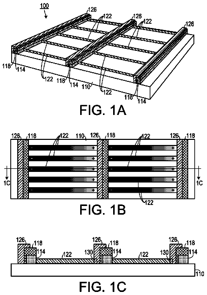
FIG. 1A is a schematic perspective view and FIG. 1B is a schematic cross sectional view of a light emitting device according to one embodiment of the present invention.
FIG. 2A is a schematic perspective view and FIG. 2B is a schematic cross sectional view of the light emitting device according to another embodiment of the present invention.
FIG. 3A is a schematic perspective view and FIG. 3B is a schematic cross sectional view of the light emitting device according to yet another embodiment of the present invention.
FIG. 4A is a schematic perspective view and FIG. 4B is a schematic cross sectional view of the light emitting device according to still another embodiment of the present invention.
FIG. 5 is a schematic perspective view of the light emitting device according to another embodiment of the present invention.
FIG. 6 is a schematic perspective view of the light emitting device according to a further embodiment of the present invention.
FIG. 7 is a schematic perspective view of the light emitting device according to still another embodiment of the present invention.
FIG. 8 is a schematic top view of the semiconductor light emitting element according to an embodiment of the present invention.
FIG. 9 is a schematic cross sectional view of the semiconductor light emitting element according to the embodiment of the present invention shown in FIG. 8.
FIG. 10 is a schematic perspective view showing two light sources mounted on a light guide plate according to an embodiment of the present invention.
FIG. 11 is a schematic cross sectional view of the light device according to the embodiment shown in FIG. 10.
FIG. 12 is a schematic plan view of a semiconductor light emitting element according to one of the examples of the present invention.
FIG. 13 is a schematic cross sectional view of a semiconductor light emitting element according to another example of the present invention.
FIG. 14 is a schematic plan view of a semiconductor light emitting element according to another example of the present invention.
FIG. 15 is a schematic plan view of a semiconductor light emitting element according to yet another example of the present invention.
FIGS. 16A, 16B, 16C and 16D are schematic cross sectional views showing the process steps for making an embodiment of the present invention.
FIG. 17A is a schematic perspective view and FIG. 17B is a schematic cross sectional view of a light emitting device according to still another embodiment of the present invention.
FIG. 18A is a schematic perspective view and FIG. 18B is a schematic cross sectional view of a light emitting device according to yet another embodiment of the present invention.
FIG. 19A is a schematic perspective view and FIG. 19B is a schematic cross sectional view of a light emitting device according to a further embodiment of the present invention.
FIG. 20A is a schematic perspective view and FIG. 20B is a schematic cross sectional view of a light emitting device according to a still further embodiment of the present invention.
FIG. 21A is a schematic perspective view and FIG. 21B is a schematic cross sectional view of a light emitting device according to another embodiment of the present invention.
FIG. 22A is a schematic perspective view and FIG. 22B is a schematic cross sectional view of a light emitting device according to still another embodiment of the present invention.
FIG. 23A is a schematic perspective view and FIG. 23B is a schematic cross sectional view of a light emitting device according to a further embodiment of the present invention.
FIG. 24A is a schematic perspective view and FIG. 24B is a schematic cross sectional view of a light emitting device according to still another embodiment of the present invention.
FIG. 25A is a schematic perspective view and FIG. 25B is a schematic cross sectional view of a light emitting device according to still another embodiment of the present invention.
FIG. 26A is a schematic perspective view and FIG. 26B is a schematic cross sectional view of a light emitting device according to a further embodiment of the present invention.
Detailed description of the preferred embodiments
After performing various tests, the inventor discovered a way for an improved mounting for a semiconductor device using an insert-type package. The package includes a portion having thermal distortion-resistant characteristics to enable the package to be positioned relative to other members. That is, in the present invention, the support part has at least a first main surface disposed adjacent to the recess for housing the semiconductor element and a second main surface disposed adjacent to and offset from the first surface. The presence of at least two main surfaces enables the positioning of the package with respect to the other members.
The present invention will be described with reference to the accompanying drawings in which preferred embodiments of the invention are shown by way of example, especially by using the example of a light emitting device. FIGS. 1-5 show schematic perspective views and schematic cross sectional views of light emitting devices according to the present invention. In addition, FIGS. 16A-16D show schematic cross sectional views of the molding process for the package of the present invention.
The light emitting device of the present invention has several embodiments. For example, as shown in FIG. 1A, a package 1 is formed by integral molding so that the end parts of both the positive and negative electrodes 2 can be inserted in the package 1. A recess is formed on a first main surface 1a of the package 1 for housing the light emitting element 4. The end portions of a positive electrode and a negative electrode are disposed on a bottom surface of the recess and are separated from each other while exposing their respective main surfaces. The gap between the positive and negative electrodes is filled with an insulating molding material.
Here, the term "main surface" in the present specification refers to a surface of the light emitting device which is on the same side as the side which emits light from the light emitting element. Furthermore, the configuration of the light emitting surface formed on the main surface of the light emitting device is not limited to a rectangular shape as shown in FIG. 1A, but can be a elliptical shape as shown in FIG. 6. With such a configuration, the light emitting surface area can be maximized while the mechanical strength of the side wall which forms the recess can be retained. This structure also enables the light emitting device to emit light into a wider area.
The positive electrode and the negative electrode of a light emitting device of the present invention are inserted so that they protrude from the side ends of the package. The protruding parts of the lead electrodes are bent rearwardly away from the main surface of the package, or they are bent toward the mounting surface perpendicular to the main surface. Here, the mounting surface is the surface that is perpendicular to the main surface of the package and that is parallel to the longer side of the recess. In this arrangement, the light emitting device of the present invention is a side light emitting type which emits light approximately parallel to the mounting surface.
The package 1 used in the present invention comprises a recess formed in the main surface and defined by an interior wall 8 of the package. A step can be formed by a side wall in the main surface of the package disposed away from the recess. More specifically, the side wall can be disposed between at least a first main surface 1a which is adjacent to the recess and a second main surface 1b which is a step lower than or set back from the first main surface 1a. That is, a step is formed between the first main surface and the second main surface. This step is not necessarily provided perpendicularly to the longer sides of the first main surface. The step may be formed at an angle to the lengthwise direction of the semiconductor element as long as it facilitates fitting or matching of the semiconductor element device of the present invention relative to an external support part or an optical member. In addition, the shape of the step is not limited in shape to a single wall between the first main surface 1a and the second main surface 1b, as the step may also have more than two or three steps, which would then include a third main surface, a fourth main surface, etc. and several side walls between them. Because of this configuration, positioning of the device relative to other optical members, can be achieved uniformly by using at least the first main surface 1a and the second main surface 1b.
Attaching an optical member such as a lens having a specific shape to the device, or assembling a surface emitting light source by combining the light emitting device of present invention with an optical guide plate can be facilitated and enhances the light intensity and obtains the desired optical properties for the light emitting device in accordance with the present invention. At this time, by providing a shape on the optical member which is capable of fitting or matching with the shape of the main surface side having at least the first main surface 1a and the second main surface 1b of the light emitting device with no space between, a light source can be assembled with ease and precision. Therefore, a light source with excellent mass productivity and excellent optical properties can be obtained.
In addition, although the main surface has a step between the first main surface 1a and the second main surface 1b in the present embodiment, the present invention is not limited to a configuration having steps. It is also possible to have a main surface where the second main surface 1b is continuous with the first main surface 1a as shown in FIGS. 18A and 18B and described further below. By fabricating the mounting surface of the other optical members so as to fit the continuous first main surface 1a and second main surface 1b with no space therebetween, the present invention provides a light emitting device having an excellent capacity for installation with other optical members.
According to the embodiment shown in FIGS. 17A and 17B, the second main surfaces are defined by the protrusions 1b on both ends of the support member 1. The protrusions 1b do not necessarily need to be formed at the ends of the support member. They may be formed at any location suitable for positioning of the semiconductor device.
The protrusions 1b also do not necessarily need to perpendicularly extend to the longer side of the support member. They may also be formed as a groove extending diagonally with respect to the longer side, instead of a protrusion, as shown in FIGS. 21A and 21B.
Additionally, as shown in FIGS. 18A and 18B, the first main surface and the second main surface are continuous and angularly offset from each other. There is a dividing line between the first main surface and the second main surface on each side of the recess. The two dividing lines on the package that separate the second main surfaces from the first main surfaces do not necessarily need to be straight lines. These dividing lines (or surface interfaces) could also be curved. Similarly, the dividing surface separating the first main surface and the second main surface in the embodiments when they are offset, do not necessarily need to be planar. These surfaces can also be curved surfaces.
FIGS. 19A and 19B and FIGS. 20A and 20B show embodiments where the second main surface can be formed as a circular recess or a protrusion, respectively. The recess or protrusion does not necessarily need to be a circular. They also may other shapes including polygonal shapes.
Furthermore the recess and the protrusion may be shaped as a circular groove as shown in FIG. 22A and FIG. 22B or as a raised circular wall as shown in FIGS. 23A and 23B. It is also possible to use differently shaped grooves, walls and/or recesses.
FIGS. 24A and 24B show an embodiment where the second main surface includes a protrusion such as a circular or elliptical protrusion.
FIGS. 25A and 25B show an embodiment where the second main surface includes a recess such as a circular or elliptical recess.
FIGS. 26A and 26B show an embodiment where the second main surface includes a protrusion which is formed so as to angularly extend between the opposed sides of the package.
As seen in the embodiments described above, the configuration defined by the first main surface and the second main surface of the present invention can be designed considering the position of the semiconductor, the viscosity of the adhesive as well as other factors.
FIGS. 16A through 16D show schematic cross sectional views showing the molding process of the package 1 according to one embodiment of the invention. The molding process of the package of the present invention is described in steps (a) through (d) below. (a) First, a lead frame 24 formed by punching a metal plate is sandwiched between the die 27 having a protrusion and the die 28 having a cavity. The lead frames 24 are placed in the resin-sealing space formed by the die 27 having a protrusion. The die 28 has a cavity so that the tip portions of the lead frames 24 are arranged so as to be opposite from each other and are spaced apart by a predetermined interval. (b) Next, as shown with the injection direction 29 of package molding member 26, the package molding member 26 is injected into the through-hole formed in the direction of the resin-sealing space, and the resin-sealing space is filled with the package molding member 26. (c) The package molding member 26 is then heated to cure the resin. (d) First, the die 28 having the cavity is removed and the pushing member 25 is shifted in a thrust direction 30 toward the second main surface 1b, which is a pin-knock face. Then the package 1 can be removed from the die 27 having a protrusion.
As described above, the package 1 formed by injection molding used in a light emitting device according to the present invention, is first formed in a mold. Then the package 1 is detached from the mold by pushing it out with a pushing member 25, such as a pin or the like, equipped in the mold.
However, when detaching the package, the molding member of the package still remains hot and is susceptible to deformation by external forces. For example, in the case wherein a main surface of the lead electrode 2 in the recess is used as a pin-knock surface, weak mechanical strength of the molding member may cause dislocation or deformation of the lead electrode 2. This can result in mounting the light emitting element 4 on a tilt, and thus the light emitting devices may not all be oriented for emitting light in the same direction. Therefore, it is necessary to arrange a pin-knock surface on the surface of the package 1.
In the case where the light emitting device is downsized, the end part of the package must be arranged as the pin-knock surface. However, it is possible that the package 1 may still be soft when detaching it from the molding die. If so, a part of the molding material may be pushed inwardly when knocked by the pin. In the case where the pin-knock surface is provided on the upper surface of the first main surface adjacent to the recess, the mold material that was pushed back may shift toward the light reflecting surface. This process causes deformation of the light reflecting surface and this may exert a damaging effect on the optical properties of the light emitting device.
In contrast, the light emitting device according to the present invention has the first main surface 1a and the second main surface 1b disposed in sequence outwardly from the recess which includes the light emitting surface. Therefore, the package can be detached from the die by arranging the second main surface as the pin-knock surface. This prevents deformation of the recess and enables mass production without causing a damaging effect to the light emitting properties.
The configuration of the second main surface 1b according to the present invention is not specifically limited. It is preferable to have an elevated portion 1c on the second main surface 1b, and it is also preferable to set the height of the elevated portion 1c to be lower than the height of the first main surface. According to this configuration, the contact area between the second main surface 1b and the adhesive member or the like, can be increased when fixing the light emitting device according to the present invention to other members, thereby enhancing their adhesion strength. Furthermore, as shown in FIGS. 2-4, it is preferable to form the external wall of the elevated portion 1c so that it is surrounding a depression. When the depression is filled with an adhesive member and it is fixed to an optical member or the like, the external wall prevents the adhesive member from flowing toward the lead electrode or the first main surface 1a. This forms a light emitting device with excellent reliability and excellent optical properties. In addition, the configuration having a protrusion 1c on the second main surface 1b can also be formed at the same time using process step (d) for removing the package 1, by pressing the pushing member 25 against the second main surface 1b.
The package 1 of an embodiment of the present invention has a recess capable of housing the light emitting element 4. The shape of the inner wall of the recess is not specifically limited. In the case where the light emitting element 4 is mounted, it is preferable to make the inner wall as a tapered wall, where its internal diameter widens toward the opening. This arrangement enables light emitted from the end face of the light emitting element 4 to pass through the light observation surface. In addition, a light reflection function can be added so as to enhance the light reflectivity, by providing a metal plating with Ag or the like on the inner surface of the recess.
In the light emitting device according to this embodiment of the present invention, the light emitting element 4 is placed in the recess of the package 1 formed as described above. Then a translucent resin is filled in the recess so as to cover the light emitting element 4 with a sealing portion 3.
In the following description, the production process and the individual components of the embodiments of the present invention will be described in more detail.
Process 1: Formation of the Lead Electrodes
In the present embodiment, the first process includes pulling a metal sheet to form a lead frame having plurality of pairs of positive and negative lead electrodes. Next, a plating operation is performed on the surface of the lead frame. In addition, a hanger lead which supports the packages throughout the production processes, from the step of lead electrode formation through the step of light emitting device partition, can be provided on a portion of the lead frame.
Lead Electrodes 2
The lead electrodes 2 in the present embodiment are electric conductors which supply power to the light emitting element and are capable of having the light emitting element mounted thereon. Particularly, the lead electrodes 2 are formed by integral molding so that one end of the lead electrode is inserted into the package and the other end protrudes from a surface of the package. In addition, the main surfaces of the end portions of the inserted electrodes 2 are exposed on the bottom surface of the recess in the package.
Although the materials for the lead electrodes 2 are not specifically limited except for related to conductivity, good adhesiveness with conductive wires 5 which form electrical connections with the semiconductor element and conductive bumps 6 as well as good electric conductivity are required. As an example of the value of the electrical resistance, 300 .mu..OMEGA.-cm or less is preferable and 3 .mu..OMEGA.-cm or less is more preferable. As for the material fulfilling such conditions, iron, copper, copper containing iron, copper containing tin, and aluminum, iron, or copper plated with gold or silver are preferably used.
In each portion of the pressed metal long sheet corresponding to a part of the package, an end face of the positive electrode is disposed so as to be separated from the negative electrode and opposite from an end face of the negative electrode. In the present embodiment, a specific process is not carried out on the lead electrode 2 where their surfaces of the end portions are exposed in the bottom face of the recess. However, the bond strength with the molding resin can be enhanced by providing at least a pair of through-holes on either side of the axis in the longitudinal direction of the recess.
Process 2: Formation of the Package
In the present embodiments a package 1 is capable of mounting a light emitting element 4. The package 1 functions as a support member for securing the lead electrodes 2 where the light emitting element 4 is mounted. The package 1 also protects the light emitting element 4 and the conductive wires 5 from the external environment.
Next, the metal long sheet described above is placed between the mold 28 having a recess and the mold 27 having a protrusion and then the molds are closed. The molding member is injected into the cavity created by the closed molds, through a gate provided at the back face of the mold having a recess. The cavity described above corresponds to the outer shape of the package. In the present embodiment, the molds for shaping the molding resin portion are provided with steps on the main surface of the package. This structure obtains a package 1 having the first main surface 1a and the second main surface 1b which is placed a step lower than the first main surface 1a, and is also further from the recess than the first main surface 1a. In addition, it is preferable to insert the pressed metal long sheet between the mold 28 having a recess and the mold 27 having a protrusion in such way so that the direction of punching coincides with that of injection of resin into the molds. According to such placement of the metal long sheet, the resin can be filled in the space formed by the end portions of the positive and negative electrodes without leaving gaps. This arrangement also prevents molding resin from flowing out onto either of the main surfaces.
Furthermore, in the case where a hanger lead is provided on the lead frame, as shown in FIG. 3A, package 1 is formed having a recess on its side face corresponding to the shape of the end portion of the hanger lead. The hanger lead can also support the package throughout the production processes.
Molding Material
The molding material for the package used in the present invention is not specifically limited. A liquid crystal polymer, a polyphthalamide resin, a polybutylene terephthalate (PBT), or the like, as well as any other known thermoplastic resins can be used. When a semi-crystalline polymer resin containing crystals of high-melting point is used such as polyphthalamide resin, a package having a large surface energy and good adhesion with a sealing resin in the recess or with an optical guide plate, can be obtained. Accordingly, interfacial separation between the package recess and the sealing resin can be prevented when they are cooled. In addition, a white pigment substance such as titanium oxide or the like, can be mixed into the molding member of a package to enhance the efficiency of the reflection of light emitted from the light emitting chip.
The molding member formed in such a manner is detached from the mold as follows. First, the mold is opened, and the pin provided in the mold having a protrusion is thrust toward the second main surface of the package. At this moment, a cylindrical wall having an inner diameter which is the same as the size of a pinhead is formed. Such a cylindrical wall can prevent the flow of adhesive material while fixing the light emitting device to other members by using an adhesive material or the like, and can achieve an enhanced adhesive force.
Process 3: Mounting of the Semiconductor Element
Next, the semiconductor element is fixed to the lead electrode 2 exposed in the bottom face of the recess formed in the package 1. In the present embodiment, a semiconductor element will be illustrated as an example of a light emitting element. However, the semiconductor element used in the present invention is not limited to this light emitting element, and can be a photodetector, an electrostatic protection element (Zener diode), or an element which is made by a combination of at least two of these elements.
Light Emitting Element 4
As an example of the semiconductor element in the present invention, a semiconductor element may be used such as a light emitting element, a light receiving element, or the like. The semiconductor element in the present embodiment can also be an LED chip used as a light emitting element.
The light emitting element 4 is not specifically limited in the present invention. In the case where a fluorescent material is concurrently used, it is preferable to use a semiconductor light emitting element having an active layer capable of emitting light with a wavelength capable of exciting the fluorescent material. As an example of such a semiconductor light emitting element, various semiconductors such as ZnSe or GaN can be used. However, a nitride semiconductor (In.sub.xAl.sub.yGa.sub.1-x-yN, 0.ltoreq.X, 0.ltoreq.Y, X+Y.ltoreq.1) capable of emitting light with a short-wavelength that can sufficiently excite the fluorescent material is preferable. The nitride semiconductor may contain boron or phosphorus if needed.
As an example of the structure of the semiconductor, a homostructure, a heterostructure or a double heterostructure having an MIS junction, a PIN junction or a P-N junction can be used. A variety of emission light wavelengths can be selected depending on the materials or the degree of the mixed crystal in the semiconductor layers. In addition, the active layer can be of a single well structure or a multiple well structure, formed as a thin film wherein a quantum effect occurs.
In the case where a nitride semiconductor is used, a material such as sapphire, spinel, SiC, Si, ZnO, GaN, or the like, is preferably used as the semiconductor substrate. It is preferable to use a sapphire substrate in order to form a nitride semiconductor having good crystallinity and which can be efficiently produced in quantity. A nitride semiconductor can be formed on the sapphire substrate in accordance with MOCVD or the like. For example, a buffer layer, such as of GaN, AlN, GaAlN, or the like, can be formed on a sapphire substrate, and a nitride semiconductor having a P-N junction can be formed thereon. Furthermore, the substrate can be removed after formation of the semiconductor layers.
An example of a light emitting element having a P-N junction using a nitride semiconductor includes, for example, a double heterostructure wherein a first contact layer of N-type gallium nitride, a first cladding layer of N-type aluminum gallium nitride, an active layer of indium gallium nitride, a second cladding layer of P-type aluminum gallium nitride, and a second contact layer of P-type gallium nitride, are layered on the buffer layer in sequence. Nitride semiconductors show N-type conductivity when in the condition where no impurities have been doped. In order to form an N-type nitride semiconductor having the desired properties such as improved light emission efficiency, it is preferable to arbitrarily introduce an N-type dopant such as Si, Ge, Se, Te, C, or the like. On the other hand, in order to form a P-type nitride semiconductor, it is preferable to dope with a P-type dopant such as Zn, Mg, Be, Ca, Sr, Ba, or the like.
Due to the fact that a nitride semiconductor is not easily converted to the P-type solely by doping a P-type dopant, it is preferable to treat such a semiconductor after introduction of the dopant in processes such as heating in a furnace or irradiation with plasma. After forming the electrodes, the semiconductor wafer is cut into chips so that the light emitting elements of the nitride semiconductor can be obtained. In addition, an insulating protective film made of materials such as SiO.sub.2 can be made by means of patterning and which covers the entire element except the bonding parts of each electrode which are exposed. Thus with this arrangement, downsized light emitting devices can be obtained with a high reliability.
In order to emit white light by using the light emitting diode of the present invention, it is preferable for the wavelength of light emitted from the light emitting element to be greater than or equal to 400 nm and less than or equal to 530 nm, and more preferably greater than or equal to 420 nm and less than or equal to 490 nm. These ranges take into consideration the complementary color relationship with fluorescent material and deterioration of the translucent resin, or the like. Furthermore, it is more preferable for the wavelength to be greater than or equal to 450 nm and less than or equal to 475 nm, in order to improve the excitation and the emission efficiency of the light emitting element and the fluorescent material. In addition, the light emitting elements having a main emission wavelength less than 400 nm, which is in ultraviolet region, or the short wavelength range of visible light can be used in combination with members relatively resistant to deterioration by ultraviolet light.
Bump 6
The light emitting element 4 in the present embodiment can obtain uniform emission when mounted by the flip tip method because there is no obstacle to shield emission at the light emitting face side. This method includes a pair of electrodes or bumps 6 provided on the same face side and placed to face a pair of lead electrodes exposed in the recess of the package. The material for the bumps 6 is not specifically limited except for its conductivity. It is preferable for the bumps 6 to contain at least one material which is included in the positive and negative electrodes of light emitting element or in the plating material of the positive and negative lead electrodes. In the present embodiment, a bump of Au is formed on each lead electrode 2, and each bump 6 and each lead electrode 2 are placed so as to be opposed to each other. Then these elements are bonded by ultrasonic soldering.
As an example of a different bump forming process, a stud bump can be obtained by cutting the wire so as to leave the edge portion of the wire after bonding an edge portion of the conductive wire. In another process, a bump can be obtained by metal deposition after forming the desired mask pattern, or the like. In addition, a bump can be provided first to the electrode side of the light emitting element, or it can be provided to both the lead electrode side and the light emitting element side, respectively.
The description continues in the full USPTO document.
 Lapsed, fee not paid3 drawings