Background of the invention
1. Field of the invention
The present invention relates to a light-emitting element which sandwiches a thin film containing a light-emitting material between electrodes and which emits light by applying current. Moreover, the present invention relates to a display device and an electronic appliance which use the light-emitting element.
2. Related art
A display using a thin film light-emitting element of a self-light-emitting type, which emits light by itself when current is applied, has been extensively developed.
This thin film light-emitting element emits light by connecting an electrode to a single-layer or multilayer thin film formed using one or both of organic compound and inorganic compound and by applying current. Such a thin film light-emitting element is expected to reduce the power consumption, occupy smaller space, and increase the visibility, and the market is also expected to expand further.
It has become possible to manufacture an element which emits light more efficiently than before by dividing the function for each layer of a light-emitting element having a multilayer structure (for example, see Reference 1: Applied Physics Letters, Vol. 51, No. 12, 913-915
by C. W. Tang et al.).
A thin film light-emitting element having a multilayer structure has a light-emitting laminated body sandwiched between an anode and a cathode. The light-emitting laminated body comprises a hole-injecting layer, a hole-transporting layer, a light-emitting layer, an electron-transporting layer, an electron-injecting layer, and the like. Among these layers, the hole-injecting layer, the hole-transporting layer, the electron-transporting layer, and the electron-injecting layer are not always employed depending on the element structure.
The hole-injecting layer in the light-emitting laminated body as above is formed by selecting a material which can inject holes comparatively easily from a metal electrode into a layer mainly containing organic compound. The electron-transporting layer in the light-emitting laminated body is formed by selecting a material being superior in electron-transporting properties. Thus, each layer in the light-emitting laminated body is formed by selecting a material superior in each function.
However, a material which can inject electrons comparatively easily from an electrode into a material mainly containing organic compound, or a material mainly containing organic compound which can transport electrons at a predetermined mobility or more are very limited. As is clear from the limitation on the material, the injection of the electrons from the electrode into the layer mainly containing the organic compound is originally rare to occur. This causes the problem that the drive voltage increases drastically over time.
Summary of the invention
Consequently, it is an object of the present invention to provide a light-emitting element having a structure in which the increase in the drive voltage over time is small.
Further, it is an object of the present invention to provide a display device in which the drive voltage is low and the increase in the drive voltage over time is small and which can resist long-term use.
According to the present invention, a layer in contact with an electrode in a light-emitting element is a hole-generating layer such as a layer containing a P-type semiconductor or an organic compound layer containing a material having electron-accepting properties, a light-emitting layer is sandwiched between the hole-generating layers, and an electron-generating layer is formed between the hole-generating layer on a cathode side and the light-emitting layer. This enables the increase in the drive voltage over time to be small.
A light-emitting element having one of structures according to the present invention comprises a pair of electrodes including an anode and a cathode, a first layer and a second layer for generating holes, a third layer containing a light-emitting material, and a fourth layer for generating electrons, wherein the third layer is sandwiched between the first layer and the second layer which are provided between the electrodes, wherein the fourth layer is provided between the third layer and the second layer, and wherein the second layer contacts the cathode.
A light-emitting element having one of structures according to the present invention comprises a pair of electrodes including an anode and a cathode, a first layer and a second layer which contain a P-type semiconductor, a third layer containing a light-emitting material, and a fourth layer containing an N-type semiconductor, wherein the third layer is sandwiched between the first layer and the second layer which are provided between the electrodes, wherein the fourth layer is provided between the third layer and the second layer, and wherein the second layer contacts the cathode.
A light-emitting element having another structure according to the present invention comprises a pair of electrodes including an anode and a cathode, a first layer and a second layer which contain a first organic compound and a material having electron-accepting properties to the first organic compound, a third layer which contains a light-emitting material, and a fourth layer which contains a second organic compound and a material having electron-donating properties to the second organic compound, wherein the third layer is sandwiched between the first layer and the second layer which are provided between the electrodes, wherein the fourth layer is provided between the third layer and the second layer, and wherein the second layer contacts the cathode.
In a light-emitting element having a structure according to the present invention, the increase in the drive voltage over time can be suppressed.
Further, a display device in which the increase in the drive voltage over time is small and which can resist long-term use can be provided.
Brief description of the drawings
In the accompanying drawings:
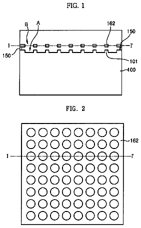
FIG. 1 shows a light-emitting element according to the present invention;
FIG. 2 shows a light-emitting element according to the present invention;
FIG. 3 shows a light-emitting element according to the present invention;
FIG. 4 shows a light-emitting element according to the present invention;
FIGS. 5A to 5E show a process for manufacturing a thin film light-emitting element according to the present invention;
FIGS. 6A to 6C show a process for manufacturing a thin film light-emitting element according to the present invention;
FIGS. 7A and 7B show an example of a structure of a display device according to the present invention;
FIGS. 8A and 8B are a top view and a cross-sectional view of a light-emitting device according to the present invention;
FIGS. 9A to 9E show examples of electronic appliances to which the present invention can be applied;
FIGS. 10A to 10C show examples of a structure of a display device according to the present invention;
FIGS. 11A to 11F show examples of a pixel circuit of a display device according to the present invention;
FIG. 12 shows an example of a protective circuit of a display device according to the present invention;
FIG. 13 is a graph showing the voltage-luminance characteristic of an element in Embodiment 1;
FIG. 14 is a graph showing the voltage-current characteristic of an element in Embodiment 1;
FIG. 15 is a graph showing the voltage-luminance characteristic of an element in Embodiment 2;
FIG. 16 is a graph showing the current density-luminance characteristic of an element in Embodiment 2;
FIG. 17 is a graph showing the voltage-current characteristic of an element in Embodiment 2;
FIG. 18 is a graph showing the change of voltage of an element over time in Embodiment 2;
FIG. 19 is a graph showing the change of luminance of an element over time in Embodiment 2;
FIG. 20 is a graph showing the voltage-luminance characteristic of an element in Embodiment 3;
FIG. 21 is a graph showing the voltage-current characteristic of an element in Embodiment 3;
FIGS. 22A to 22C show absorption spectra of a complex material containing .alpha.-NPD and molybdenum oxide;
FIGS. 23A to 23C show absorption spectra of a complex material containing DNTPD and molybdenum oxide;
FIG. 24 is a graph showing a relation between an optical distance and current efficiency; and
FIG. 25 is a graph showing an optical distance and a light-emission spectrum.
Detailed description of the invention
Embodiment Modes and Embodiments are hereinafter described with reference to the drawings. However, since the present invention can be carried out with many different modes, it is to be understood by those skilled in the art that the modes and details can be modified without departing from the scope of the present invention. Therefore, the present invention is not construed as being limited to the description of the following Embodiment Modes and Embodiments.
Embodiment Mode 1
The present embodiment mode describes the structure of a light-emitting element of the present invention with reference to FIGS. 1 and 2. In a light-emitting element according to the present invention, a light-emitting layer 104 containing a light-emitting material and an electron-generating layer 105 are stacked, and the light-emitting layer 104 and the electron-generating layer 105 are sandwiched between a first hole-generating layer 102 and a second hole-generating layer 103. The first hole-generating layer 102 and the second hole-generating layer 103 are further sandwiched between an anode 101 and a cathode 106, and stacked over an insulator 100 such as a substrate or an insulating film. Over the insulator 100 such as the substrate or the insulating film, the anode 101, the first hole-generating layer 102, the light-emitting layer 104, the electron-generating layer 105, the second hole-generating layer 103, and the cathode 106 are stacked in order (FIG. 1). Alternatively, the order may be opposite: the cathode 106, the second hole-generating layer 103, the electron-generating layer 105, the light-emitting layer 104, the first hole-generating layer 102, and the anode 101 are stacked in order (FIG. 2).
The first hole-generating layer 102 and the second hole-generating layer 103 may be formed either with different materials or with the same material. For example, a layer containing both of a hole-transporting material and an electron-accepting material which can receive electrons from the hole-transporting material, a P-type semiconductor layer, or a layer containing a P-type semiconductor is used. As the hole-transporting material, for example, an aromatic amine compound (having a bond of a benzene ring with nitrogen), phthalocyanine (abbreviated to H.sub.2Pc), or a phthalocyanine compound such as copper phthalocyanine (abbreviated to CuPc) or vanadyl phthalocyanine (abbreviated to VOPc) can be used. The aromatic amine compound is, for example, 4,4'-bis[N-(1-naphthyl)-N-phenyl-amino]-biphenyl (abbreviated to .alpha.-NPD), 4,4'-bis[N-(3-methylphenyl)-N-phenyl-amino]-biphenyl (abbreviated to TPD), 4,4',4''-tris(N,N-diphenyl-amino)-triphenylamine (abbreviated to TDATA), 4,4',4''-tris[N-(3-methylphenyl)-N-phenyl-amino]-triphenylamine (abbreviated to MTDATA), 4,4'-bis(N-(4-(N,N-di-m-tolylamino)phenyl)-N-phenylamino)biphenyl (abbreviated to DNTPD), 1,3,5-tris[N,N-di(m-tolyl)amino]benzene (abbreviated to m-MTDAB), or 4,4',4''-tris(N-carbazolyl)triphenylamine (abbreviated to TCTA). As the electron-accepting material which can receive electrons from the hole-transporting material, for example, vanadium oxide, molybdenum oxide, 7,7,8,8,-tetracyanoquinodimethane (abbreviated to TCNQ), 2,3-dicyanonaphtoquinone (abbreviated to DCNNQ), 2,3,5,6-tetrafluoro-7,7,8,8,-tetracyanoquinodimethane (abbreviated to F.sub.4-TCNQ), or the like is given. The electron-accepting material is selected which can receive electrons in accordance with the combination with the hole-transporting material. Further, metal oxide such as molybdenum oxide, vanadium oxide, ruthenium oxide, cobalt oxide, nickel oxide, or copper oxide can be used as the P-type semiconductor.
As the electron-generating layer 105, a layer containing both of an electron-transporting material and an electron donating material which can donate electrons to the electron-transporting material, an N-type semiconductor layer, or a layer containing an N-type semiconductor can be used. As the electron-transporting material, for example, the following can be used; a metal complex having a quinoline skeleton or a benzoquinoline skeleton such as tris-(8-quinolinolato)aluminum (abbreviated to Alq.sub.3), tris(4-methyl-8-quinolinolato)aluminum (abbreviated to Almq.sub.3), bis(10-hydroxybenzo[h]-quinolinolato)beryllium (abbreviated to BeBq.sub.2), or bis(2-methyl-8-quinolinolato)-4-phenylphenolato-aluminum (abbreviated to BAlq). Besides, a metal complex having an oxazole or thiazole ligand such as bis[2-(2-hydroxyphenyl)benzoxazolate]zinc (abbreviated to Zn(BOX).sub.2) or bis[2-(2-hydroxyphenyl)benzothiazolate]zinc (abbreviated to Zn(BTZ).sub.2) can be used. In addition to the metal complex, 2-(4-biphenylyl)-5-(4-tert-butylphenyl)-1,3,4-oxadiazole (abbreviated to PBD), 1,3-bis[5-(p-tert-butylphenyl)-1,3,4-oxadiazole-2-yl]benzene (abbreviated to OXD-7), 3-(4-tert-butylphenyl)-4-phenyl-5-(4-biphenylyl)-1,2,4-triazole (abbreviated to TAZ), 3-(4-tert-butylphenyl)-4-(4-ethylphenyl)-5-(4-biphenylyl)-1,2,4-triazole (abbreviated to p-EtTAZ), bathophenanthroline (abbreviated to BPhen), bathocuproin (abbreviated to BCP), or the like can be used. As the electron donating material which can donate electrons to the electron-transporting material, for example, alkali metal such as lithium or cesium, magnesium, alkali-earth metal such as calcium, or rare-earth metal such as erbium or ytterbium can be used. The electron donating material which can donate electrons is selected in accordance with the combination with the electron-transporting material. Further, a metal compound such as metal oxide can be used as the N-type semiconductor, and for example zinc oxide, zinc sulfide, zinc selenide, titanium oxide, or the like can be used.
The light-emitting layer 104 containing the light-emitting material is divided into two types. One of them is a layer in which a light-emitting material to be a luminescence center is diffused in a layer formed with a material having a wider energy gap than the light-emitting material. The other one is a layer consisting of a light-emitting material. The former structure is preferred because the concentration quenching is difficult to occur. As the light-emitting material to be the luminescence center, the following can be employed; 4-dicyanomethylene-2-methyl-6-[2-(1,1,7,7-tetramethyl-9-julolidyl)ethenyl- )-4H-pyran (abbreviation: DCJT); 4-dicyanomethylene-2-t-butyl-6-[2-(1,1,7,7-tetramethyl-julolidine-9-yl)et- henyl]-4H-pyran; periflanthene; 2,5-dicyano-1,4-bis[2-(10-methoxy-1,1,7,7-tetramethyl-julolidine-9-yl)eth- enyl]benzene, N,N'-dimethylquinacridone (abbreviated to DMQd), coumarin 6, coumarin 545T, tris(8-quinolinolato)aluminum (abbreviated to Alq.sub.3), 9,9'-bianthryl, 9,10-diphenylanthracene (abbreviated to DPA), 9,10-bis(2-naphthyl)anthracene (abbreviated to DNA), 2,5,8,11-tetra-t-butylperylene (abbreviated to TBP), or the like. As the material to be a base material in the case of forming the layer in which the light-emitting material is diffused, the following can be used; an anthracene derivative such as 9,10-di(2-naphtyl)-2-tert-butylanthracene (abbreviated to t-BuDNA), a carbazole derivative such as 4,4'-bis(N-carbazolyl)biphenyl (abbreviated to CBP), or a metal complex such as tris(8-quinolinolato)aluminum (abbreviated to Alq.sub.3), tris(4-methyl-8-quinolinolato)aluminum (abbreviated to Almq.sub.3), bis(10-hydroxybenzo[h]-quinolinato)beryllium (abbreviated to BeBq.sub.2), bis(2-methyl-8-quinolinolato)-4-phenylphenolato-aluminum (abbreviated to BAlq), bis[2-(2-hydroxyphenyl)pyridinato]zinc (abbreviated to Znpp.sub.2), or bis[2-(2-hydroxyphenyl)benzoxazolate]zinc (abbreviated to ZnBOX). As the material which can constitute the light-emitting layer 104 singularly, tris(8-quinolinolato)aluminum (abbreviated to Alq.sub.3), 9,10-bis(2-naphtyl)anthracene (abbreviated to DNA), or bis(2-methyl-8-quinolinolato)-4-phenylphenolato-aluminum (abbreviated to BAlq) or the like can be used.
The light-emitting layer 104 may be formed either in a single-layer structure or a multilayer structure. A hole-transporting layer may be provided between the first hole-generating layer 102 and the layer in which the light-emitting material is diffused in the light-emitting layer 104. Further, an electron-transporting layer may be provided between the electron-generating layer 105 and the layer in which the light-emitting material is diffused in the light-emitting layer 104. These layers are not necessarily provided. Alternatively, only one of the hole-transporting layer and the electron-transporting layer may be provided. The materials of the hole-transporting layer and the electron-transporting layer conform to those of the hole-transporting layer in the hole-generating layer and the hole-transporting layer in the electron-generating layer respectively; therefore, the description is omitted here. Refer to the description of those layers.
The anode 101 is preferably formed with metal, alloy, an electrically conductive compound each of which has high work function (work function of 4.0 eV or more), or mixture of these. As a specific example of the anode material, the following can be used; ITO (indium tin oxide), ITO containing silicon, IZO (indium zinc oxide) in which zinc oxide (ZnO) is mixed by 2 to 20% into indium oxide, gold (Au), platinum (Pt), nickel (Ni), tungsten (W), chromium (Cr), molybdenum (Mo), iron (Fe), cobalt (Co), copper (Cu), palladium (Pd), or metal nitride such as TiN. Meanwhile, as the cathode material used for forming the cathode 106, it is preferable to use metal, alloy, an electrically conductive compound each of which has low work function (work function of 3.8 eV or less), or mixture of these. As the specific example of the cathode material, the following can be used; an element belonging to group 1 or 2 in the periodic table; alkali metal such as Li or Cs, Mg, or alkali-earth metal such as Ca or Sr. In addition, alloy containing the above element such as Mg:Ag or Al:Li, a compound containing the above element such as LiF, CsF, or CaF.sub.2, or transition metal containing rare-earth metal can also be used. Further, a multilayer containing the above element and another metal (including alloy) such as Al, Ag, or ITO can be used.
In addition to the anode 101, the first hole-generating layer 102, the light-emitting layer 104, the electron-generating layer 105, the second hole-generating layer 103, and the cathode 106, the light-emitting layer may have a hole-injecting layer 107 between the anode 101 and the first hole-generating layer 102 (FIGS. 3 and 4). A phthalocyanine compound is effective for the hole-injecting layer 107. For example, phthalocyanine (abbreviated to H.sub.2--Pc), copper phthalocyanine (abbreviated to Cu--Pc), or the like can be used.
The above material is just an example, and the material can be selected appropriately by a practitioner as long as the advantage of the present invention is obtained.
In the light-emitting element having the above structure according to the present invention, holes are injected from the second hole-generating layer 103 into the second electrode by applying voltage. In addition, electrons are injected from the electron-generating layer 105 into the light-emitting layer 104. Further, holes are injected from the first hole-generating layer 102 into the light-emitting layer 104. Then, the injected electrons and holes are recombined in the light-emitting layer, and light emission is obtained when the excited light-emitting material returns to the ground state. Here, in the light-emitting element according to the present invention, the electrons are not injected from the electrode into the layer mainly containing the organic compound but injected from the layer mainly containing the organic compound into the layer mainly containing the organic compound. The electrons are difficult to be injected from the electrode into the layer mainly containing the organic compound. In the conventional light-emitting element, the drive voltage has increased when the electrons are injected from the electrode into the layer mainly containing the organic compound. However, since the light-emitting element according to the present invention does not have such a process, the light-emitting element having low drive voltage can be provided. Moreover, it is already known from the experiment that the drive voltage increases over time more drastically when the light-emitting element has higher drive voltage; therefore, the light-emitting element having low drive voltage also serves as a light-emitting element in which the increase in the drive voltage over time is small.
Embodiment Mode 2
Another embodiment mode of the present invention is described. The present embodiment mode describes an example of improving the characteristic of a viewing angle of a light-emitting element and a display device by appropriately adjusting the thicknesses of the first hole-generating layer 102 and the second hole-generating layer 103. Since the multilayer structure and the material of the light-emitting element in the present embodiment mode are the same as those in Embodiment Mode 1, the description is omitted here. Refer to Embodiment Mode 1.
Light emitted from the light-emitting element include light directly emitted from the light-emitting layer 104 and light emitted after being reflected once or multiple times. The light directly emitted and the light emitted after being reflected interfere in accordance with the relation between their phases so that they are intensified or attenuated with each other. Therefore, the light emitted from the light-emitting element is light which has been combined as a result of the interference.
The phase of light reflected when entering a medium having high refractive index from a medium having low refractive index is inverted. For this reason, in the light-emitting element having the structure shown in Embodiment Mode 1, the phase of light is inverted when the light is reflected at the interface between the electrode such as the anode 101 or the cathode 106 and the layer in contact with the electrode. When the light reflected at the electrode interferes with the light emitted from the light-emitting layer, it is possible to decrease the change of the spectrum shape which occurs depending on the angle of viewing a surface from which light is extracted and to increase the current efficiency of the light-emitting element, provided that the optical distance (refractive index.times.physical distance) between the light-emitting layer and the electrode satisfies (2m-1).lamda./4 (m is a natural number of 1 or more and .lamda. is a center wavelength of the light emitted from the light-emitting layer). The current efficiency shows the luminance with respect to the flowed current. When the current efficiency is higher, predetermined luminance can be obtained even with a smaller amount of current. Moreover, the deterioration of the element tends to be little.
Since the reflection is small between films whose gap of refractive index is small, the reflections except the reflection at the interface between the electrode and the film in contact with the electrode are ignorable. Therefore, in this embodiment mode, attention is paid only to the reflection between the electrode and the film in contact with the electrode.
In the case of a light-emitting element in which light is extracted from the side of the anode 101, the light is reflected at the cathode 106. For this reason, in order to increase the current efficiency of the light-emitting element and to decrease the change of the spectrum shape which occurs depending on the angle of viewing the surface from which the light is extracted, the optical distance (refractive index.times.physical distance) from the light-emission position to the surface of the cathode 106 needs to be (2m-1).lamda./4 (m is a natural number of 1 or more and .lamda. is a center wavelength of the light emitted from the light-emitting layer).
The light-emitting layer 104 may be formed in a single-layer structure with a layer containing a light-emitting material, or may be formed in a multilayer structure including a layer such as an electron-transporting layer or a hole-transporting layer and a layer containing a light-emitting material. The layer containing the light-emitting material may be a layer in which a light-emitting material to be a luminescence center is diffused or may be a layer consisting of a light-emitting material.
A plurality of layers formed with different materials are provided between the light-emission position and the cathode 106. In this embodiment mode, the plurality of layers correspond to the electron-generating layer 105 and the second hole-generating layer 103. A part of the layer containing the light-emitting material that corresponds to a half thickness thereof can be regarded as a layer positioned between the light-emission position and the cathode 106. In the case of forming the light-emitting layer with a plurality of layers, more layers formed with different materials may be included. In such a structure, the optical distance from the light-emission position to the cathode 106 can be calculated by multiplying the thicknesses and the refractive indexes of the respective films and summing up the products. The total is set so as to be (2m-1).lamda./4 (m is a natural number of 1 or more and .lamda. is a center wavelength of the light emitted from the light-emitting layer). That is to say, the following formula
is satisfied. In the formula (1), the layer containing the light-emitting material is assumed to be 1 and the cathode 106 is assumed to be j (j is an integer number of 4 or more), and the layers existing between the layer containing the light-emitting material and the cathode 106 are denoted with numerals in order from the layer containing the light-emitting material. Moreover, the refractive index n and the thickness d with a certain numeral given thereto indicate the refractive index and the thickness of the layer to which the same numeral is given (that is, n.sub.1 is the refractive index of the layer containing the light-emitting material and d.sub.j is the thickness of the cathode).
.times..times..times..ltoreq..times..times..lamda..ltoreq..times..times..- times..times..times..times. ##EQU00001##
Here, it is necessary to adjust the film thickness in order to satisfy the formula (1). Since the layer mainly containing the organic compound has low electron mobility, the drive voltage increases when the electron-transporting material and the electron-generating layer 105 in which electrons serve as the carrier are thick. Consequently, in this embodiment mode, the thickness of the second hole-generating layer 103 in which the mobility is comparatively high in the layer mainly containing the organic compound is adjusted, whereby the formula
is satisfied without drastically increasing the drive voltage.
In the case of a light-emitting element in which light is extracted from the side of the cathode 106, the light is reflected at the anode 101. Therefore, in order to increase the current efficiency of the light-emitting element and to decrease the change of the spectrum shape which occurs depending on the angle of viewing the surface from which the light is extracted, the optical distance (refractive index.times.physical distance) from the light-emission position to the surface of the anode 101 may be set to (2m-1).lamda./4 (m is a natural number of 1 or more and .lamda. is a center wavelength of the light emitted from the light-emitting layer).
The light-emitting layer 104 may be formed either in a single-layer structure of the layer containing the light-emitting material or in a multilayer structure including the layer containing the light-emitting material and the layer such as the electron-transporting layer or the hole-transporting layer. The layer containing the light-emitting material may be a layer in which the light-emitting material to be the light-emission center is diffused, or a layer consisting of the light-emitting material. However, in any one of the above-mentioned structures, the layer containing the light-emitting material has a certain degree of thickness and an infinite number of the luminescence centers exist; therefore, it is impossible to determine the exact position where the light emission occurs. Accordingly, in this embodiment mode, a position of a part of the film containing the light-emitting material that corresponds to a half thickness thereof is regarded as the position where the light-emission occurs.
One or a plurality of layers are provided between the position where the light-emission occurs and the anode 101. In this embodiment mode, the layer corresponds to the first hole-generating layer 102. Further, it can be said that a part of the layer containing the light-emitting material that corresponds to a half thickness thereof is also the layer located between the position where the light-emission occurs and the anode 101. Moreover, more layers may be included in the case where the light-emitting layer is formed with a plurality of layers. In such a structure, the optical distance from the light-emission position to the anode 101 can be calculated by multiplying the thicknesses and the refractive indexes of the respective films and summing up the products. That is to say, the following formula
is satisfied. In the formula (2), the layer containing the light-emitting material is assumed to be 1 and the anode 101 is assumed to be j (j is an integer number of 4 or more), and the layers existing between the layer containing the light-emitting material and the anode 101 are denoted with numerals in order from the layer containing the light-emitting material. Moreover, the refractive index n and the thickness d with a certain numeral given thereto indicate the refractive index and the thickness of the layer to which the same numeral is given (that is, n.sub.1 is the refractive index of the layer containing the light-emitting material and d.sub.j is the thickness of the anode).
.times..times..times..ltoreq..times..times..lamda..ltoreq..times..times..- times..times..times..times. ##EQU00002##
Here, it is necessary to adjust the film thickness in order to satisfy the formula (2). In this embodiment mode, the formula
can be satisfied without drastically increasing the drive voltage, by adjusting the thickness of the first hole-generating layer 102 in which the mobility is comparatively high in the layer mainly containing the organic compound.
In the case of the structure in which light is extracted from both of the anode 101 and the cathode 106, both of the formulas
and
may be satisfied.
With the structure of the light-emitting element shown in this embodiment mode, it is possible to provide a light-emitting element in which the change of the light-emission spectrum which occurs depending on the angle of viewing the surface from which the light is extracted is decreased.
The present embodiment mode can be combined with Embodiment Mode 1.
Embodiment Mode 3
This embodiment mode describes a display device according to the present invention shown in Embodiment Mode 1 or Embodiment Mode 2 while showing its manufacturing method with reference to FIGS. 5A to 6C. Although this embodiment mode shows an example of manufacturing an active matrix display device, a light-emitting element of the present invention is also applicable for a passive matrix display device.
First, a first base insulating layer 51a and a second base insulating layer 51b are formed over a substrate 50, and then a semiconductor layer is formed over the second base insulating layer 51b (FIG. 5A).
As a material of the substrate 50, glass, quartz, plastic (such as polyimide, acrylic, polyethylene terephthalate, polycarbonate, polyacrylate, or polyethersulfone), or the like can be used. These substrates may be used after being polished by CMP or the like as necessary. In this embodiment mode, a glass substrate is used.
The first base insulating layer 51a and the second base insulating layer 51b are provided in order to prevent an element which adversely affects the characteristic of the semiconductor film such as alkali metal or alkali-earth metal in the substrate 50 from diffusing into the semiconductor layer. As the material of these base insulating layers, silicon oxide, silicon nitride, silicon oxide containing nitrogen, silicon nitride containing oxygen, or the like can be used. In this embodiment mode, the first base insulating layer 51a is formed with silicon nitride, and the second base insulating layer 51b is formed with silicon oxide. Although the base insulating layer is formed in a two-layer structure including the first base insulating layer 51a and the second base insulating layer 51b in this embodiment mode, the base insulating layer may be formed in a single-layer structure or a multilayer structure including three or more layers. The base insulating layer is not necessary when the diffusion of the impurity from the substrate does not lead to a significant problem.
In this embodiment mode, the semiconductor layer formed subsequently is obtained by crystallizing an amorphous silicon film with a laser beam. The amorphous silicon film is formed in 25 to 100 nm thick (preferably 30 to 60 nm thick) over the second base insulating layer 51b by a known method such as a sputtering method, a reduced-pressure CVD method, or a plasma CVD method. After that, heat treatment is conducted for one hour at 500.degree. C. for dehydrogenation.
Next, the amorphous silicon film is crystallized with a laser irradiation apparatus to form a crystalline silicon film. In this embodiment mode, an excimer laser is used at the laser crystallization. After the emitted laser beam is shaped into a linear beam spot using an optical system, the amorphous silicon film is irradiated with the linear beam spot. Thus, the crystalline silicon film is formed which is to be used as the semiconductor layer.
Alternatively, the amorphous silicon film can be crystallized by another method such as a method in which the crystallization is conducted only by heat treatment or a method in which heat treatment is conducted using a catalyst element for inducing the crystallization. As the element for inducing the crystallization, nickel, iron, palladium, tin, lead, cobalt, platinum, copper, gold, or the like is given. By using such an element, the crystallization is conducted at lower temperature in shorter time than the crystallization only by the heat treatment; therefore, the damage to the glass substrate is suppressed. In the case of crystallizing only by the heat treatment, a quartz substrate which can resist the high temperature is preferably used as the substrate 50.
Subsequently, a small amount of impurity elements are added to the semiconductor layer as necessary in order to control the threshold, which is so-called channel doping. In order to obtain the required threshold, an impurity showing N-type or P-type (such as phosphorus or boron) is added by an ion-doping method or the like.
After that, as shown in FIG. 5A, the semiconductor layer is patterned into a predetermined shape so that an island-shaped semiconductor layer 52 is obtained. The patterning is conducted by etching the semiconductor layer using a mask. The mask is formed in such a way that a photo resist is applied to the semiconductor layer and the photo resist is exposed and baked so that a resist mask having a desired mask pattern is formed over the semiconductor layer.
Next, a gate insulating layer 53 is formed so as to cover the semiconductor layer 52. The gate insulating layer 53 is formed in 40 to 150 nm thick with an insulating layer containing silicon by a plasma CVD method or a sputtering method. In this embodiment mode, silicon oxide is used.
Then, a gate electrode 54 is formed over the gate insulating layer 53. The gate electrode 54 may be formed with an element selected from the group consisting of tantalum, tungsten, titanium, molybdenum, aluminum, copper, chromium, and niobium, or may be formed with an alloy material or a compound material which contains the above element as its main component. Further, a semiconductor film typified by a poly-crystalline silicon film doped with an impurity element such as phosphorus may be used. Ag--Pd--Cu alloy may also be used.
Although the gate electrode 54 is formed with a single layer in this embodiment mode, the gate electrode 54 may have a multilayer structure including two or more layers of, for example, tungsten as a lower layer and molybdenum as an upper layer. Even in the case of forming the gate electrode in the multilayer structure, the above-mentioned material is preferably used. The combination of the above materials may also be selected appropriately. The gate electrode 54 is processed by etching with the use of a mask formed with a photo resist.
Subsequently, impurities are added to the semiconductor layer 52 at high concentration using the gate electrode 54 as the mask. According to this step, a thin film transistor 70 comprising the semiconductor layer 52, the gate insulating layer 53, and the gate electrode 54 is formed.
The manufacturing process of the thin film transistor is not limited in particular, and may be modified appropriately so that a transistor having a desired structure can be manufactured.
Although this embodiment mode employs a top-gate thin film transistor using the crystalline silicon film obtained by the laser crystallization, a bottom-gate thin film transistor using an amorphous semiconductor film can also be applied to a pixel portion. Not only silicon but also silicon germanium can be used for the amorphous semiconductor. In the case of using silicon germanium, the concentration of germanium preferably ranges from approximately 0.01 to 4.5 atomic %.
Moreover, a microcrystal semiconductor (semi-amorphous semiconductor) film which includes crystal grains each having a diameter of 0.5 to 20 nm in the amorphous semiconductor may also be used. The microcrystal having the crystal with a diameter of 0.5 to 20 nm is also referred to as a so-called microcrystal (.mu.c).
Semi-amorphous silicon (also referred to as SAS), which belongs to the semi-amorphous semiconductor, can be obtained by decomposing silicide gas according to glow discharging. As typical silicide gas, SiH.sub.4 is given. Besides, Si.sub.2H.sub.6, SiH.sub.2Cl.sub.2, SiHCl.sub.3, SiCl.sub.4, SiF.sub.4, or the like can be used. By using the silicide gas after diluting the silicide gas with hydrogen or hydrogen and one or plural kinds of noble gas selected from the group consisting of helium, argon, krypton, and neon, SAS can be easily formed. The silicide gas is preferably diluted with the dilution ratio of 1:10 to 1:1000. The reaction to form the film by the decomposition according to glow discharging may be conducted at the pressure ranging from 0.1 to 133 Pa. The electric power for forming the glow discharging may be supplied at high frequency in the range of 1 to 120 MHz, preferably 13 to 60 MHz. The substrate heat temperature is preferably 300.degree. C. or less, preferably in the range of 100 to 250.degree. C.
The raman spectrum of thus formed SAS shifts to the side of lower wavenumber than 520 cm.sup.-1. According to X-ray diffraction, diffraction peaks of a silicon crystal lattice are observed at
The description continues in the full USPTO document.
 Lapsed, fee not paid7 drawings

