Background of the invention
1. Field of the invention
The present invention relates to an OLED (organic light emitting diode) panel obtained by forming an OLED on a substrate and sealing the OLED between the substrate and a cover member. The invention also relates to an OLED module in which an IC including a controller, or the like, is mounted to the OLED panel. In this specification, `light emitting device` is the generic term for the OLED panel and for the OLED module. Electronic equipment using the light emitting device is also included in the present invention.
2. Description of the related art
Being self-luminous, OLEDs eliminate the need for a backlight that is necessary in liquid crystal display devices (LCDs), and thus they are most suitable when manufacturing thinner devices. Also, the self-luminous OLEDs are high in visibility and have no limit in terms of viewing angle. These are the reasons for the attention that light emitting devices using the OLEDs are receiving in recent years as display devices to replace CRTs and LCDs.
An OLED has a layer containing an organic compound (organic light emitting material) that provides luminescence (electroluminescence) when an electric field is applied (the layer is hereinafter referred to as organic light emitting layer), in addition to an anode layer and a cathode layer. Luminescence obtained from organic compounds is classified into light emission upon return to the base state from singlet excitation (fluorescence) and light emission upon return to the base state from triplet excitation (phosphorescence). A light emitting device according to the present invention can use one or both types of the light emission.
In this specification, all the layers that are provided between an anode and a cathode together make an organic light emitting layer. Specifically, the organic light emitting layer includes a light emitting layer, a hole injection layer, an electron injection layer, a hole transporting layer, an electron transporting layer, etc. A basic structure of an OLED is a laminate of an anode, a light emitting layer, and a cathode layered in this order. The basic structure can be modified into a laminate of an anode, a hole injection layer, a light emitting layer, and a cathode layered in this order, or a laminate of an anode, a hole injection layer, a light emitting layer, an electron transporting layer, and a cathode layered in this order.
The problem in putting a light emitting device into practice is lowering in luminance of OLED which accompanies degradation of its organic light emitting material.
Organic light emitting materials are weak against moisture, oxygen, light, and heat, which accelerate degradation of the organic light emitting materials. Specifically, the rate of degradation of an organic light emitting material depends on the structure of a device for driving the light emitting device, characteristics of the organic light emitting material, materials of electrodes, manufacture process conditions, how the light emitting device is driven, etc.
Even when the voltage applied to the organic light emitting layer is constant, the luminance of the OLED is lowered as the organic light emitting layer degrades, and an image displayed therefore becomes unclear. In this specification, a voltage applied to an organic light emitting layer from a pair of electrodes is called an OLED drive voltage (Ve1).
When an image is displayed in color by using three types of OLEDs that respectively emit red (R) light, green (G) light, and blue (B) light, different organic materials are used to form organic light emitting layers of OLEDs of different colors. Accordingly, the rate of degradation of organic light emitting layer may vary between OLEDs of different colors. Then the difference in luminance between OLEDs of different colors will be noticeably large as time passes, making it impossible for the light emitting device to display an image in desired colors.
The temperature of organic light emitting layer is influenced by the outside temperature and heat generated from the OLED panel itself. Generally, the amount of current flowing in an OLED varies depending on the temperature. FIG. 26 shows a change in voltage-current characteristic of an OLED when the temperature of its organic light emitting layer is changed. With the voltage kept constant, the OLED drive current is increased as the temperature of the organic light emitting layer rises. Since the OLED drive current is in proportion to the OLED luminance, the luminance of the OLED becomes higher as the OLED drive current becomes larger. Since a change in temperature of the organic light emitting layer thus causes a change in OLED luminance, displaying an image in desired gray scales is difficult and current consumption of the light emitting device is increased accompanying a temperature rise.
Generally, temperature change brings varying degrees of changes in OLED drive current to different types of organic light emitting materials and, therefore, in color display, the luminance could be changed by temperature change differently for OLEDs of different colors. It is impossible to obtain desired colors when OLEDs of different colors lose their luminance balance.
Summary of the invention
The present invention has been made in view of the above, and an object of the present invention is therefore to provide a light emitting device capable of keeping the luminance constant and displaying an image in desired colors without being influenced by degradation of its organic light emitting layer or by temperature change.
The present inventors have taken notice of the fact that the luminance of OLED is lowered by degradation less when light is emitted with a current flow to an OLED kept constant than when light is emitted with the OLED drive voltage kept constant. (In this specification, a current flowing into an OLED is called an OLED drive current (Ie1).) Then, the present inventors have thought of preventing a change in OLED luminance due to degradation of OLED by controlling the OLED luminance with current instead of voltage.
Specifically, a current mirror circuit composed of transistors is provided in each pixel in the present invention. The current mirror circuit is used to control the OLED drive current. A first transistor and a second transistor of the current mirror circuit are connected such that the drain current of the first transistor is kept substantially equal to the drain current of the second transistor irrespective of the load resistance value.
A drain current I.sub.1 of the first transistor is controlled by a signal line driving circuit. The amount of drain current I.sub.1 of the first transistor is always equal to the amount of drain current I.sub.2 of the second transistor irrespective of the load resistance value. Accordingly, the drain current I.sub.2 of the second transistor is controlled by the signal line driving circuit.
The second transistor is connected to an OLED with a single or plural circuit elements interposed therebetween, so that the drain current I.sub.2 thereof flows into the OLED. Therefore the value of OLED drive current flowing into the OLED is controlled by the signal line driving circuit irrespective of the load resistance value. In other words, the OLED drive current can be controlled to have a desired value without being influenced by difference in characteristics of transistors or degradation of OLED.
With the above structure, the present invention can prevent the luminance of OLED from lowering even when the organic light emitting layer is degraded and therefore can display a clear image. If the light emitting device is to display an image in color using OLEDs of different colors and the rate of degradation of organic light emitting layer varies between the OLEDs of different colors, the present invention is capable of keeping the luminance of light of different colors balanced and display in desired colors.
Furthermore, the present invention can set the OLED drive current to a desired value despite a change in temperature of the organic light emitting layer due to the outside temperature and heat generated from the OLED panel itself. Since the OLED drive current is in proportion to the OLED luminance, the luminance of OLED can be prevented from changing and current consumption accompanying a temperature rise can be avoided. If the light emitting device is to display an image in color, the luminance of the OLEDs of different colors can be prevented from changing to keep the luminance of light of different colors balanced and display in desired colors.
Generally, temperature change brings varying degrees of changes in OLED drive current to different types of organic light emitting materials and, therefore, in color display, the luminance could be changed by temperature change differently for OLEDs of different colors. However, the light emitting device of the present invention can obtain a desired luminance irrespective of temperature change to thereby keep the luminance of light of different colors balanced. An image thus can be displayed in desired colors.
In a common light emitting device, the electric potential of a wiring line used to supply a current to pixels is slightly lowered as the wiring line becomes longer because of the resistance of the wiring line itself. This electric potential is lowered to widely varying degrees depending on an image to be displayed. When the ratio of higher gray scale pixels to all of the pixels that receive a current from the same wiring line is large, in particular, the current flowing through the wiring lines is increased in amount to make lowering of electric potential noticeable. When the electric potential is lowered, a smaller voltage is applied to the OLED of each pixel to reduce the amount of current supplied to each pixel. Therefore, the amount of current supplied to one pixel is changed as well as the gray scale number thereof when the gray scale number of other pixels that receive a current from the same wiring line as the one pixel is changed, making it impossible for the one pixel to keep a constant gray scale. In the light emitting device of the present invention, on the other hand, a measured value and a reference value are obtained to correct the OLED current each time a new image is displayed. Therefore, a desired gray scale number is obtained for every new image through correction.
In the light emitting device of the present invention, a transistor used in a pixel may be one formed from single crystal silicon or may be a thin film transistor formed from polycrystalline silicon or amorphous silicon.
Brief description of the drawings
In the accompanying drawings:
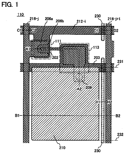
FIG. 1 is a block diagram showing a top view of a light emitting device of the present invention;
FIG. 2 is a circuit diagram of a pixel in a light emitting device of the present invention;
FIGS. 3A and 3B are timing charts of signals inputted to scanning lines;
FIGS. 4A and 4B are schematic diagrams of a pixel being driven:
FIG. 5 is a timing chart showing at which points writing periods and display periods are started in an analog driving method;
FIG. 6 is a timing chart showing at which points writing periods and display periods are started in a digital driving method;
FIG. 7 is a circuit diagram of a pixel in a light emitting device of the present invention;
FIG. 8 is a circuit diagram of a pixel in a light emitting device of the present invention;
FIGS. 9A to 9D are diagrams showing a method of manufacturing a light emitting device according to the present invention;
FIGS. 10A to 10C are diagrams showing a method of manufacturing a light emitting device according to the present invention;
FIGS. 11A and 11B are diagrams showing a method of manufacturing a light emitting device according to the present invention;
FIG. 12 is a top view of a pixel in a light emitting device of the present invention;
FIG. 13 is a sectional view of a pixel in a light emitting device of the present invention;
FIGS. 14A and 14B are diagrams showing a method of manufacturing a light emitting device according to the present invention;
FIG. 15 is a top view of a pixel in a light emitting device of the present invention;
FIG. 16 is a top view of a pixel in a light emitting device of the present invention;
FIG. 17 is a block diagram of a signal line driving circuit:
FIG. 18 is a detailed diagram of a signal line driving circuit in a digital driving method;
FIG. 19 is a circuit diagram of a current setting circuit in a digital driving method;
FIG. 20 is a block diagram of a scanning line driving circuit;
FIG. 21 is a timing chart showing at which points writing periods and display periods are started in a digital driving method;
FIG. 22 is a timing chart showing at which points writing periods and display periods are started in a digital driving method;
FIG. 23 is a timing chart showing at which points writing periods and display periods are started in a digital driving method;
FIGS. 24A to 24C are diagrams showing the exterior and sectional views of a light emitting device of the present invention;
FIGS. 25A to 25H are diagrams of electronic equipment using a light emitting device of the present invention;
FIG. 26 is a graph showing the voltage-current characteristic of an OLED:
FIG. 27 is a sectional view of a pixel in a light emitting device of the present invention;
FIG. 28 is a top view of an element substrate in a light emitting device of the present invention;
FIG. 29 is an enlarged view of an element substrate in a light emitting device of the present invention;
FIGS. 30A to 30C are circuit diagrams of pixels in a light emitting device of the present invention; and
FIGS. 31A and 31B are detailed diagrams of a signal line driving circuit in a digital driving method.
Detailed description of the preferred embodiments
Embodiment Mode 1
FIG. 1 is a block diagram showing the structure of an OLED panel of the present invention. Reference symbol 100 denotes a pixel portion. The pixel portion has a plurality of pixels 101 that form a matrix. Denoted by 102 and 103 are a signal line driving circuit and a scanning line driving circuit, respectively.
In FIG. 1, the signal line driving circuit 102 and the scanning line driving circuit 103 are formed on the same substrate on which the pixel portion 100 is formed. However, the present invention is not limited to this structure. The signal line driving circuit 102 and the scanning line driving circuit 103 may be formed on a substrate that is connected through an FPC or other connectors to a substrate on which the pixel portion 100 is formed. Although the panel in FIG. 1 has one signal line driving circuit 102 and one scanning line driving circuit 103, the present invention is not limited thereto. The number of signal line driving circuits and scanning line driving circuits to be provided is freely determined by a designer.
In this specification, connection means electric connection.
In FIG. 1, the pixel portion 100 is provided with signal lines S1 to Sx, power supply lines V1 to Vx, and scanning lines G1 to Gy. The number of signal lines may not always match the number of power supply lines. The pixel portion may have other wiring lines than these wiring lines.
The power supply lines V1 to Vx are kept at a given electric potential. Although shown in FIG. 1 is the structure of a light emitting device for displaying a monochromatic image, the present invention can be applied to a light emitting device for displaying a color image. In this case, not all of the power supply lines V1 to Vx may be kept at the same level of electric potential and power supply lines for one color may have a different level of electric potential than power supply lines for another color.
FIG. 2 shows a detailed structure of the pixels 101 illustrated in FIG. 1. A pixel shown in FIG. 2 is one of the pixels 101. The pixel 101 has a signal line Si (one of S1 to Sx), a scanning line Gj (one of G1 to Gy), and a power supply line Vi (one of V1 to Vx).
Each of the pixels 101 has, at least, a transistor Tr1 first current controlling transistor or a first transistor), a transistor Tr2 (a second current controlling transistor or a second transistor), a transistor Tr3 (a third current controlling transistor or a third transistor), a transistor Tr4 (a first switching transistor or a fourth transistor), a transistor Tr5 (a second switching transistor or a fifth transistor), an OLED 104, and a storage capacitor 105.
Gate electrodes of the transistor Tr4 and of the transistor Tr5 are connected to the scanning line Gj.
The transistor Tr4 has a source region and a drain region one of which is connected to the signal line Si and the other of which is connected to a drain region of the transistor Tr1. The transistor Tr5 has a source region and a drain region one of which is connected to the signal line Si and the other of which is connected to a gate electrode of the transistor Tr3.
Gate electrodes of the transistor Tr1 and of the transistor Tr2 are connected to each other. Source regions of the transistor Tr1 and of the transistor Tr2 are connected to the power supply line Vi.
The gate electrode of the transistor Tr2 is connected to a drain region thereof. The drain region of the transistor Tr2 is connected to a source region of the transistor Tr3.
A drain region of the transistor Tr3 is connected to a pixel electrode of the OLED 104. The OLED 104 has an anode and a cathode. In this specification, the cathode is called an opposite electrode (second electrode) when the anode is used as a pixel electrode (first electrode) and, when the cathode serves as the pixel electrode, the anode is called the opposite electrode.
The electric potential of the power supply line Vi (power supply electric potential) is kept constant. The electric potential of the opposite electrode is also kept constant.
The transistor Tr4 may be an n-channel transistor or a p-channel transistor and the same applies to the transistor Tr5. However, the transistor Tr4 and the transistor Tr5 have to have the same polarity.
The transistor Tr1 may be an n-channel transistor or a p-channel transistor and the same applies to the transistors Tr2 and Tr3. However, the transistors Tr1, Tr2, and Tr3 have to have the same polarity. When the pixel electrode serves as an anode and the opposite electrode serves as a cathode, the transistors Tr1, Tr2, and Tr3 are p-channel transistors. On the other hand, n-channel transistors are used for the transistors Tr1, Tr2, and Tr3 when the opposite electrode serves as an anode and the pixel electrode serves as a cathode.
The storage capacitor 105 is formed between the gate electrode of the transistor Tr3 and the power supply line Vi. The storage capacitor 105 is provided to maintain the voltage between the gate electrode of the transistor Tr3 and the source region thereof (gate voltage) more securely but it may not always be necessary.
The transistors Tr1 and Tr2 may have storage capacitor s between their gate electrodes and the power supply line so that the gate voltages of the transistors Tr1 and Tr2 can be maintained more securely.
Next, driving of the light emitting device of the present invention will be described with reference to FIGS. 3A to 4B. The description on driving of the light emitting device of the present invention can be divided into a description for a writing period Ta and a description for a display period Td. FIGS. 3A and 3B are timing charts of scanning lines. A period in which a scanning line is selected, in other words, a period in which every transistor whose gate electrode is connected to the selected scanning line is turned ON, is expressed as ON. On the other hand, a period in which a scanning line is not selected, in other words, a period in which every transistor whose gate electrode is connected to the scanning line is turned OFF, is expressed as OFF. FIGS. 4A and 4B schematically show connection of the transistor Tr1, the transistor Tr2 and the transistor Tr3 during a writing period Ta and a display period Td.
In a writing period Ta, the scanning lines G1 to Gy are selected in order as shown in FIG. 3A. Then a constant current Ic flows between the signal lines S1 to Sx and the power supply lines V1 to Vx in accordance with the electric potential of a video signal inputted to the signal line driving circuit 102. In this specification, the current Ic is called a signal current.
FIG. 4A shows a schematic diagram of one of the pixels 101 when the constant current Ic flows in the signal line Si in a writing period Ta. Denoted by 106 is a terminal for connecting the pixel to a power supply for giving an electric potential to the opposite electrode. 107 denotes a constant current supply of the signal line driving circuit 102.
The transistors Tr4 and Tr5 are ON and, when the signal line Si receives the constant current Ic, the constant current Ic flows between the drain region of the transistor Tr1 and the source region thereof. The amount of the constant current Ic is controlled by the constant current supply 107 so that the transistor Tr1 operates in a saturation range. In the saturation range, V.sub.GS is given as the electric potential difference between the gate electrode and the source region (gate voltage), .mu. is given as the mobility of the transistor, C.sub.O as the gate capacitance per unit area, W/L as the ratio of a channel width W of the channel formation region to a channel length L thereof, V.sub.TH as the threshold, and I.sub.1 as the drain current of the transistor Tr1. Then the following Equation 1 is obtained. I.sub.1=.mu.C.sub.OW/L(V.sub.GS-V.sub.TH).sup.2/2 Equation 1
In Equation 1, .mu., C.sub.O, W/L, and V.sub.TH are values fixed for the respective transistors. The drain current I.sub.1 of the transistor Tr1 is also kept constant at Ic by the constant current supply 107. Accordingly, the gate voltage V.sub.GS of the transistor Tr1 is determined by the value of the current Ic as shown in Equation 1.
The gate electrode of the transistor Tr2 is connected to the gate electrode of the transistor Tr1. The source region of the transistor Tr2 is connected to the source region of the transistor Tr1. Therefore the gate voltage of the transistor Tr2 is equal to the gate voltage of the transistor Tr1. Accordingly, a drain current I.sub.2 of the transistor Tr2 is kept at the same level as the drain current of the transistor Tr1 to satisfy I.sub.2=Ic.
The drain current of the transistor Tr3 is equal to the drain current I.sub.2 of the transistor Tr2. Satisfying Equation 1, the transistor Tr3 generates a gate voltage in an amount according to the drain current I.sub.2.
The drain current I.sub.2 of the transistor Tr2 thus flows into the OLED 104 through a channel formation region of the transistor Tr3. Accordingly, the OLED drive current is equal to the constant current Ic set by the constant current supply 107.
The OLED 104 emits light at a luminance according to the amount of OLED drive current. When the OLED drive current is extremely close to 0 or when the OLED drive current flows in the reverse bias direction, the OLED 104 does not emit light.
After all of the scanning lines G1 to Gy are selected and the above operation is conducted on pixels in every line, the writing period Ta is ended. As the writing period Ta is ended, a display period Td is started.
FIG. 3B is a timing chart of the scanning lines in the display period Td. In the display period Td, none of the scanning lines G1 to Gy are selected.
FIG. 4B is a schematic diagram of a pixel in the display period Td. The transistors Tr4 and Tr5 are turned OFF. The source regions of the transistor Tr1 and of the transistor Tr2 are connected to the power supply line Vi and kept at a given electric potential (power supply electric potential).
In the display period Td, the drain region of the transistor Tr1 is in a so-called floating state in which Tr1 does not receive an electric potential from other wiring lines nor from a power supply. On the other hand, the transistors Tr2 and Tr3 maintain V.sub.GS set in the writing period Ta, which means that the drain current I.sub.2 of the transistor Tr2 is still kept at Ic and that the transistor Tr3 remains ON. Therefore the OLED drive current set in the writing period Ta is maintained during the display period Td and the OLED 104 emits light at a luminance according to the amount of the OLED drive current.
In the case of a driving method using an analog video signal (analog driving method), the amount of Ic is determined in accordance with an analog video signal and the OLED 104 emits light at a luminance according to the amount of Ic to obtain a gray scale. In this case, one writing period Ta and one display period Td constitute one frame period, and one image is displayed in one frame period.
FIG. 5 is an example of the timing chart in an analog driving method. One frame period has y line periods, and one scanning line is selected in each line period. Constant currents Ic (Ic1 to Icx) flow in signal lines in each line period. In FIG. 5, Ic1[Lj] to Icx[Lj] represent values of signal current flowing in the respective signal lines in a line period Lj (j=1 to y).
Starting points of the writing period Ta and the display period Td vary between different lines and the starting point of a writing period for one line does not coincide with the starting point for another line. When the display period Td is completed for all of the pixels, one image is displayed.
In the case of a time gray scale driving method using a digital video signal (digital driving method), on the other hand, a writing period Ta and a display period Td are repeatedly alternated in one frame period to make it possible to display one image. If an image is displayed using n bit video signals, one frame period has at least n writing periods and n display periods. The n writing periods (Ta1 to Tan) are respectively associated with n bits of the n bit video signals, and so are the n display periods (Td1 to Tdn).
FIG. 6 shows at which points the n writing periods (Ta1 to Tan) and the n display periods (Td1 to Tdn) are started in one frame period. The axis of abscissa indicates time and the axis of ordinate indicates positions of scanning lines of pixels.
A writing period Tam (m is an arbitrary number ranging from 1 to n) is followed by a display period associated with the same bit number as the writing period Tam, in this case, a display period Tdm. One writing period Ta and one display period Td constitute one sub-frame period SF. A sub-frame period SFm consists of the wiring period Tam and the display period Tdm that are associated with the m-th bit signal.
Lengths of sub-frame periods SF1 to SFn are set so as to satisfy SF1:SF2: . . . :SFn=2.sup.0:2.sup.1: . . . :2.sup.n-1.
A sub-frame period having a long display period may further be divided to improve the quality of an image displayed. Specifics on how such a sub-frame period is divided can be found in Japanese Patent Application No. 2000-26716-1.
The driving method shown in FIG. 6 obtains gray scale display by controlling the sum of lengths of display periods in one frame period in which a pixel emits light.
With the above structure, the present invention can prevent the luminance of OLED from lowering even when the organic light emitting layer is degraded and therefore can display a clear image. If the light emitting device is to display an image in color using OLEDs of different colors and the rate of degradation of organic light emitting layer varies between the OLEDs of different colors, the present invention is capable of keeping the luminance of light of different colors balanced and display in desired colors.
Furthermore, the present invention can set the OLED drive current to a desired value despite a change in temperature of the organic light emitting layer due to the outside temperature and heat generated from the OLED panel itself. Since the OLED drive current is in proportion to the OLED luminance, the luminance of OLED can be prevented from changing and current consumption accompanying a temperature rise can be avoided. If the light emitting device is to display an image in color, the luminance of the OLEDs of different colors can be prevented from changing to keep the luminance of light of different colors balanced and display in desired colors.
Generally, temperature change brings varying degrees of changes in OLED drive current in accordance with different types of organic light emitting materials and, therefore, in color display, the luminance could be changed by temperature change differently for OLEDs of different colors. However, the light emitting device of the present invention can obtain a desired luminance irrespective of temperature change to thereby keep the luminance of light of different colors balanced. An image thus can be displayed in desired colors.
In a common light emitting device, the electric potential of a wiring line used to supply a current to pixels is slightly lowered as the wiring line becomes longer because of the resistance of the wiring line itself. This electric potential is lowered to widely varying degrees depending on an image to be displayed. When the ratio of higher gray scale pixels to all of the pixels that receive a current from the same wiring line is large, in particular, the current flowing through the wiring lines is increased in amount to make lowering of electric potential noticeable. When the electric potential is lowered, a smaller to voltage is applied to the OLED of each pixel to reduce the amount of current supplied to each pixel. Therefore, the amount of current supplied to one given pixel is changed as well as the gray scale number thereof when the gray scale number of other pixels that receive a current from the same wiring line as the one pixel is changed, making it impossible for the one pixel to keep a constant gray scale. In the light emitting device of the present invention, on the other hand, a measured value and a reference value are obtained to correct the OLED current each time a new image is displayed. Therefore a desired gray scale number is obtained for every new image through correction.
Embodiment Mode 2
This embodiment mode describes a structure different from the one in FIG. 2 for the pixels 101 of FIG. 1.
The pixel structure of this embodiment mode is shown in FIG. 7. A pixel shown in FIG. 7 is one of the pixels 101. The pixel 101 has a signal line Si (one of S1 to Sx), a scanning line Gj (one of G1 to Gy), and a power supply line Vi (one of V1 to Vx).
Each of the pixels 101 has, at least, a transistor Tr1 (a first current controlling transistor or a first transistor), a transistor Tr2 (a second current controlling transistor or a second transistor), a transistor Tr3 (a third current controlling transistor or a third transistor), a transistor Tr4 (a first switching transistor or a fourth transistor), a transistor Tr5 (a second switching transistor or a fifth transistor), an OLED 104, and a storage capacitor 105.
Gate electrodes of the transistor Tr4 and of the transistor Tr5 are connected to the scanning line Gj.
The transistor Tr4 has a source region and a drain region one of which is connected to the signal line Si and the other of which is connected to a drain region of the transistor Tr1. The transistor Tr5 has a source region and a drain region one of which is connected to the drain region of the transistor Tr1 and the other of which is connected to a gate electrode of the transistor Tr3.
Gate electrodes of the transistor Tr1 and of the transistor Tr2 are connected to each other. Source regions of the transistor Tr1 and of the transistor Tr2 are connected to the power supply line Vi.
The gate electrode of the transistor Tr2 is connected to a drain region thereof. The drain region of the transistor Tr2 is connected to a source region of the transistor Tr3.
A drain region of the transistor Tr3 is connected to a pixel electrode of the OLED 104. The electric potential of the power supply line Vi (power supply electric potential) is kept constant. The electric potential of the opposite electrode is also kept constant.
The transistor Tr4 may be an n-channel transistor or a p-channel transistor and the same applies to the transistor Tr5. However, the transistor Tr4 and the transistor Tr5 have to have the same polarity.
The transistor Tr1 may be an n-channel transistor or a p-channel transistor and the same applies to the transistors Tr2 and Tr3. However, the transistors Tr1, Tr2, and Tr3 have to have the same polarity. When the pixel electrode serves as an anode and the opposite electrode serves as a cathode, the transistors Tr1, Tr2, and Tr3 are p-channel transistors. On the other hand, n-channel transistors are used for the transistors Tr1, Tr2, and Tr3 when the opposite electrode serves as an anode and the pixel electrode serves as a cathode.
The storage capacitor 105 is formed between the gate electrode of the transistor Tr3 and the power supply line Vi. The storage capacitor 105 is provided to maintain the gate voltage of the transistor Tr3 more securely but it may not always be necessary.
The transistors Tr1 and Tr2 may have storage capacitor s between their gate electrodes and the power supply line so that the gate voltages of the transistors Tr1 and Tr2 can be maintained more securely.
As in the case of the pixel shown in FIG. 2, the description on operation of a light emitting device that has the pixel of FIG. 7 can be divided into a description for a writing period Ta and a description for a display period Td. The pixel in FIG. 7 operates the same way as the pixel in FIG. 2 in the writing period Ta and the display period Td. Therefore the descriptions given in Embodiment Mode 1 on FIGS. 3A to 4B apply to the pixel in FIG. 7 and will not be repeated here.
Embodiment Mode 3
This embodiment mode describes a structure different from those in FIGS. 2 and 7 for the pixels 101 of FIG. 1.
The pixel structure of this embodiment mode is shown in FIG. 8. A pixel shown in FIG. 8 is one of the pixels 101. The pixel 101 has a signal line Si (one of S1 to Sx), a scanning line Gj (one of G1 to Gy), and a power supply line Vi (one of V1 to Vx).
Each of the pixels 101 has, at least, a transistor Tr1 (a first current controlling transistor or a first transistor), a transistor Tr2 (a second current controlling transistor or a second transistor), a transistor Tr3 (a third current controlling transistor or a third transistor), a transistor Tr4 (a first switching transistor or a fourth transistor), a transistor Tr5 (a second switching transistor or a fifth transistor), an OLED 104, and a storage capacitor 105.
Gate electrodes of the transistor Tr4 and of the transistor Tr5 are connected to the scanning line Gj.
The transistor Tr4 has a source region and a drain region one of which is connected to the signal line Si and the other of which is connected to a gate electrode of the transistor Tr3. The transistor Tr5 has a source region and a drain region one of which is connected to the gate electrode of the transistor Tr3 and the other of which is connected to a drain region of the transistor Tr1.
Gate electrodes of the transistor Tr1 and of the transistor Tr2 are connected to each other. Source regions of the transistor Tr1 and of the transistor Tr2 are connected to the power supply line Vi.
The gate electrode of the transistor Tr2 is connected to a drain region thereof. The drain region of the transistor Tr2 is connected to a source region of the transistor Tr3.
A drain region of the transistor Tr3 is connected to a pixel electrode of the OLED 104. The electric potential of the power supply line Vi (power supply electric potential) is kept constant. The electric potential of the opposite electrode is also kept constant.
The transistor Tr4 may be an n-channel transistor or a p-channel transistor and the same applies to the transistor Tr5. However, the transistor Tr4 and the transistor Tr5 have to have the same polarity.
The transistor Tr1 may be an n-channel transistor or a p-channel transistor and the same applies to the transistors Tr2 and Tr3. However, the transistors Tr1, Tr2, and Tr3 have to have the same polarity. When the pixel electrode serves as an anode and the opposite electrode serves as a cathode, the transistors Tr1, Tr2, and Tr3 are p-channel transistors. On the other hand, n-channel transistors are used for the transistors Tr1, Tr2, and Tr3 when the opposite electrode serves as an anode and the pixel electrode serves as a cathode.
The storage capacitor 105 is formed between the gate electrode of the transistor Tr3 and the power supply line Vi. The storage capacitor 105 is provided to maintain the voltage between the gate electrode of the transistor Tr3 and the source region thereof (gate voltage) more securely but it may not always be necessary.
The transistors Tr1 and Tr2 may have storage capacitor s between their gate electrodes and the power supply line so that the gate voltages of the transistors Tr1 and Tr2 can be maintained more securely.
As in the case of the pixel shown in FIG. 2, the description on operation of a light emitting device that has the pixel of FIG. 8 can be divided into a description for a writing period Ta and a description for a display period Td. The pixel in FIG. 8 operates the same way as the pixel in FIG. 2 in the writing period Ta and the display period Td. Therefore the descriptions given in Embodiment Mode 1 on FIGS. 3A to 4B apply to the pixel in FIG. 8 and will not be repeated here.
Embodiments
Embodiments of the present invention are described hereinafter.
Embodiment 1
Next, described with reference to FIGS. 9 to 13 is a method of forming the light emitting device of the present invention. Here, the method of simultaneously forming, on the same substrate, transistors Tr2, Tr3 and Tr5 of the pixel, and transistors of a driving portion provided surrounding the pixel portion is described in detail according to steps. In addition, transistors Tr1 and Tr4 can be manufactured according to the manufacturing method of transistors Tr2, Tr3, and Tr5. The pixels shown in FIGS. 7, 8, 30A, 30B, and 30C can also be manufactured according to the manufacturing method shown in this embodiment.
This embodiment uses a substrate 900 of a glass such as barium borosilicate glass or aluminoborosilicate glass as represented by the glass #7059 or the glass #1737 of Corning Co. There is no limitation on the substrate 900 provided it has a property of transmitting light, and there may be used a quartz substrate. There may be further used a plastic substrate having heat resistance capable of withstanding the treatment temperature of this embodiment.
Referring next to FIG. 9 (A), an underlying film 901 comprising an insulating film such as silicon oxide film, silicon nitride film or silicon oxynitride film is formed on the substrate 900. In this embodiment, the underlying film 901 has a two-layer structure. There, however, may be employed a structure in which a single layer or two or more layers are laminated on the insulating film. The first layer of the underlying film 901 is a silicon oxynitride film 901a formed maintaining a thickness of from 10 to 200 nm (preferably, from 50 to 100 nm) relying upon a plasma CVD method by using SiH.sub.4, NH.sub.3 and N.sub.2O as reaction gases. In this embodiment, the silicon oxynitride film 901a (having a composition ratio of Si=32%, O=27%, N=24%, H=17%) is formed maintaining a thickness of 50 nm. The second layer of the underlying film 901 is a silicon oxynitride film 901b formed maintaining a thickness of from 50 to 200 nm (preferably, from 100 to 150 nm) relying upon the plasma CVD method by using SiH.sub.u and N.sub.2O as reaction gases. In this embodiment, the silicon oxynitride film 901b (having a composition ratio of Si=32%, O=59%, N=7%, H=2%) is formed maintaining a thickness of 100 nm.
The description continues in the full USPTO document.
 Lapsed, fee not paid4 drawings