Background
The present disclosure relates to semiconductor devices and methods for manufacturing semiconductor devices, and more particularly, to semiconductor devices including a metal-insulator-semiconductor field-effect transistor (MISFET) having source/drain regions including a silicon compound layer, and methods for fabricating the semiconductor devices.
A technique of enhancing the drive capability of a MISFET (hereinafter referred to as a "MIS transistor") by applying a stress to the channel region of the MIS transistor has been employed so as to improve the performance of a semiconductor integrated circuit device. For p-type MIS transistors, it is known that if a compressive stress is applied to the channel region in the gate length direction, the mobility of carriers is increased, whereby the drive capability of the p-type MIS transistor is enhanced. For example, a compressive stress may be applied to the channel region in the gate length direction by forming, in the source/drain regions, a SiGe layer having a larger lattice constant than that of the silicon substrate (see, for example, PATENT DOCUMENT 1: Japanese Patent Publication No. 2006-196549, NON-PATENT DOCUMENT 1: T. Ghani et al., "A 90 nm High Volume Manufacturing Logic Technology Featuring Novel 45 nm Gate Length Strained Silicon CMOS Transistors," IEDM Tech. Digest, pp. 978-980, 2003, and NON-PATENT DOCUMENT 2: Z. Luo et al., "Design of High Performance PFETs with Strained Si Channel and Laser Anneal," IEDM Tech. Digest, pp. 495-498, 2005).
A method for fabricating a conventional semiconductor device including a p-type MIS transistor having p-type source/drain regions including a SiGe layer and an n-type MIS transistor will be described hereinafter with reference to FIGS. 8A-8C, 9A-9C, and 10A-10C. FIGS. 8A-10C are cross-sectional views showing the conventional semiconductor device as viewed in the gate length direction, in the order in which the semiconductor device is fabricated. In FIGS. 8A-10C, the term "pMIS region" shown on the left side refers to a region where the p-type MIS transistor is formed, and the term "nMIS region" shown on the right side refers to a region where the n-type MIS transistor is formed.
Initially, as shown in FIG. 8A, an isolation region 101 is selectively formed in an upper portion of a semiconductor substrate 100. As a result, a first active region 100a surrounded by the isolation region 101 is formed in the pMIS region of the semiconductor substrate 100. A second active region 100b surrounded by the isolation region 101 is formed in the nMIS region of the semiconductor substrate 100. Thereafter, an n-type well region 102a is formed in the pMIS region of the semiconductor substrate 100. On the other hand, a p-type well region 102b is formed in the nMIS region of the semiconductor substrate 100.
Next, on the first and second active regions 100a and 100b, a first and a second gate electrode formation portion 105A and 105B are formed which include a first and a second gate insulating film 103a and 103b, a first and a second gate electrode 104a and 104b, and a first and a second protective insulating film 105a and 105b made of a silicon oxide film.
Next, first and second offset spacers 106a and 106b made of a silicon oxide film are formed on side surfaces of the first and second gate electrode formation portions 105A and 105B. Thereafter, p-type and n-type extension injection regions 107a and 107b are formed in the first and second active regions 100a and 100b laterally outside the first and second gate electrode formation portions 105A and 105B (i.e., are formed in the first and second active regions 100a and 100b adjacent to the channel region and extending laterally away from it).
Next, as shown in FIG. 8B, first and second sidewalls 109A and 109B including first and second inner sidewalls 108a and 108b made of a silicon oxide film, and first and second outer sidewalls 109a and 109b made of a silicon nitride film, are formed on side surfaces of the first and second gate electrode formation portions 105A and 105B, with the first and second offset spacers 106a and 106b being interposed between the first and second inner sidewalls 108a and 108b and the side surfaces of the first and second gate electrode formation portions 105A and 105B.
Next, as shown in FIG. 8C, an insulating film 110 made of a silicon oxide film is formed on an entire surface of the semiconductor substrate 100.
Next, as shown in FIG. 9A, a resist pattern (not shown) which exposes the pMIS region and covers the nMIS region is formed on the insulating film 110 by a lithography process. Thereafter, the insulating film 110 is etched by dry etching using the resist pattern as a mask. As a result, a surface of the first active region 100a is exposed. On the other hand, the insulating film 110 which covers the second gate electrode formation portion 105B and the first sidewalls 109B is left on the second active region 100b. In this case, unnecessary sidewalls 110a are left on side surfaces of the first sidewalls 109A. Thereafter, the resist pattern is removed.
Next, as shown in FIG. 9B, the first active region 100a is etched using the sidewalls 110a and the insulating film 110 as a mask. As a result, trenches 111 are formed in the first active region 100a laterally outside the sidewalls 110a.
Next, as shown in FIG. 9C, a SiGe layer 112 doped with a p-type impurity is formed in the trenches 111. Because the SiGe layer 112 is doped with the p-type impurity, the regions of the SiGe layer 112 are p-type impurity-introduced regions.
Next, as shown in FIG. 10A, the first and second protective insulating films 105a and 105b (silicon oxide film), the sidewalls 110a (silicon oxide film), and the insulating film 110 (silicon oxide film) are removed. As a result, upper surfaces of the first and second gate electrodes 104a and 104b, and the first and second sidewalls 109A and 109B, are exposed.
Next, as shown in FIG. 10B, n-type source/drain implanted regions 113 are formed in the second active region 100b laterally outside the second sidewalls 109B.
Next, as shown in FIG. 10C, a thermal treatment is performed. As a result, the p-type impurity contained in the p-type extension injection regions 107a is activated to form p-type extension regions 114a. The n-type impurity contained in the n-type extension injection regions 107b is activated to form n-type extension regions 114b. The p-type impurity contained in the regions (p-type impurity-introduced regions) of the SiGe layer 112 is activated to form p-type source/drain regions 115a. The n-type impurity contained in the n-type source/drain implanted regions 113 is activated to form n-type source/drain regions 115b.
Thereafter, although not shown, a first and a second silicide layer are formed on the first and second gate electrodes 104a and 104b, and a third and a fourth silicide layer are formed on the p-type and n-type source/drain regions 115a and 115b.
Thus, the conventional semiconductor device is fabricated.
Summary
However, the conventional semiconductor device has the following problems.
When a compressive stress is applied to the channel region of the p-type MIS transistor in the gate length direction, the drive capability of the p-type MIS transistor is enhanced. In contrast to this, when a compressive stress is applied to the channel region of the n-type MIS transistor in the gate length direction, the drive capability of the n-type MIS transistor is degraded. Therefore, for a semiconductor device including a p-type and an n-type MIS transistor on the same semiconductor substrate, it is necessary that while a SiGe layer be formed in the source/drain regions of the p-type MIS transistor, a SiGe layer not be formed in the source/drain regions of the n-type MIS transistor.
Therefore, in the conventional semiconductor device, a SiGe layer is prevented from being formed in the n-type source/drain regions as follows. As shown in FIG. 8C, the insulating film 110 is formed an entire surface of the semiconductor substrate 100. Thereafter, as shown in FIG. 9A, a portion of the insulating film 110 which has been formed in the pMIS region is etched. As a result, a surface of the first active region 100a is exposed. On the other hand, the insulating film 110 is left on the second active region 100b. The remaining insulating film 110 prevents the formation of trenches in the second active region 100b laterally outside the second sidewalls 109B, i.e., the formation of a SiGe layer in the trenches (i.e., a SiGe layer is prevented from being formed in the n-type source/drain regions 115b).
However, as shown in FIG. 9A, when a portion of the insulating film 110 which has been formed in the pMIS region is etched, not all the portion is removed, so that unnecessary sidewalls 110a are left on the side surfaces of the first sidewalls 109A. Therefore, as shown in FIG. 9B, the trenches 111 are formed in the first active region 100a laterally outsides the sidewalls 110a, but not laterally outsides the first sidewalls 109A. Therefore, as shown in FIG. 9C, the SiGe layer 112 is formed in the first active region 100a laterally outsides the sidewalls 110a. Therefore, the SiGe layer 112 cannot be formed in the first active region 100a close to the channel region, so that a compressive stress caused by the SiGe layer 112 cannot be effectively applied to the channel region of the first active region 100a in the gate length direction.
The present disclosure describes implementations of a semiconductor device including a first MIS transistor having source/drain regions including a silicon compound layer, and a second MIS transistor, in which the silicon compound layer can be formed closer to the channel region of the first MIS transistor.
A semiconductor device according to a first aspect of the present disclosure includes a first MIS transistor and a second MIS transistor. The first MIS transistor includes a first gate insulating film formed on a first active region in a semiconductor substrate, a first gate electrode formed on the first gate insulating film, first sidewalls each including a first inner sidewall formed on a side surface of the first gate electrode and having an L-shaped cross-section, and first source/drain regions of a first conductivity type formed in the first active region laterally outside the first sidewalls. The second MIS transistor includes a second gate insulating film formed on a second active region in the semiconductor substrate, a second gate electrode formed on the second gate insulating film, second sidewalls each including a second inner sidewall formed on a side surface of the second gate electrode and having an L-shaped cross-section, and second source/drain regions of a second conductivity type formed in the second active region laterally outside the second sidewalls. The first source/drain regions include a silicon compound layer which is formed in trenches provided in the first active region and causes a first stress in a gate length direction of a channel region in the first active region. A width of the first inner sidewall is smaller than a width of the second inner sidewall.
According to the semiconductor device of the first aspect of the present disclosure, the silicon compound layer is formed using the first inner sidewall having a smaller width than that of the second inner sidewall. Therefore, the silicon compound layer can be formed in the first active region closer to the channel region. Therefore, the first stress can be effectively applied in the gate length direction of the channel region in the first active region, whereby the drive capability of the first MIS transistor can be effectively enhanced.
In addition, the second source/drain region is formed using the second inner sidewall having a larger width than that of the first inner sidewall. Therefore, the second source/drain region can be formed in the second active region further away from the channel region, whereby an increase in leakage current can be reduced in the second MIS transistor.
In the semiconductor device of the first aspect of the present disclosure, a space between the first gate electrode and the silicon compound layer is preferably smaller than the width of the second inner sidewall.
The semiconductor device of the first aspect of the present disclosure preferably further includes a first silicide layer formed on the first gate electrode, and a second silicide layer formed on the second gate electrode. A height of an upper surface of the first silicide layer is preferably lower than a height of an upper surface of the second silicide layer.
The semiconductor device of the first aspect of the present disclosure preferably further includes first offset spacers each formed between the first gate electrode and a corresponding one of the first inner sidewalls and having an I-shaped cross-section, and second offset spacers each formed between the second gate electrode and a corresponding one of the second inner sidewalls and having an I-shaped cross-section.
In the semiconductor device of the first aspect of the present disclosure, a thickness of the first inner sidewall is preferably substantially the same as or smaller than a thickness of the second inner sidewall.
In the semiconductor device of the first aspect of the present disclosure, the first sidewalls each preferably further include a first middle sidewall which is formed on a corresponding one of the first inner sidewalls and has an L-shaped cross-section. The second sidewalls each preferably further include a second middle sidewall which is formed on a corresponding one of the second inner sidewalls and has an L-shaped cross-section. A lower tip of the first middle sidewall is preferably located further away from the first gate electrode than a lower tip of the first inner sidewall.
The semiconductor device of the first aspect of the present disclosure preferably further includes a first stress insulating film which is formed on the first active region to cover the first gate electrode and the first sidewalls, and causes a stress in the same direction as that of the first stress, in the gate length direction of the channel region in the first active region.
In the semiconductor device of the first aspect of the present disclosure, the first MIS transistor is preferably a p-type MIS transistor, and the first stress is preferably a compressive stress.
The semiconductor device of the first aspect of the present disclosure preferably further includes a second stress insulating film which is formed on the second active region to cover the second gate electrode and the second sidewalls and causes a second stress in a direction opposite to that of the first stress, in a gate length direction of a channel region in the second active region.
In the semiconductor device of the first aspect of the present disclosure, the second MIS transistor is preferably an n-type MIS transistor, and the second stress is preferably a tensile stress.
The semiconductor device of the first aspect of the present disclosure preferably further includes a third MIS transistor including a third gate insulating film formed on a third active region in the semiconductor substrate, a third gate electrode formed on the third gate insulating film, third sidewalls formed on side surfaces of the third gate electrode, and third source/drain regions of the first conductivity type formed in the third active region laterally outside the third sidewalls. The third sidewalls preferably include third inner sidewalls formed on the side surfaces of the third gate electrode and having an L-shaped cross-section, third middle sidewalls formed on the third inner sidewalls and having an L-shaped cross-section, and third outer sidewalls formed on the third middle sidewalls. The first sidewall and the second sidewall preferably do not have an outer sidewall. A silicon compound layer is preferably not formed in the third source/drain regions. A width of the third inner sidewall is preferably larger than the width of the first inner sidewall.
Thus, the third source/drain region is formed using the third inner sidewall having a larger width than that of the first inner sidewall. Therefore, the third source/drain region can be formed in the third active region further away from the channel region, whereby an increase in leakage current can be reduced in the third MIS transistor.
The semiconductor device of the first aspect of the present disclosure preferably further includes a protective insulating film formed on the third gate electrode. A silicide layer is preferably not formed on the third gate electrode.
A semiconductor device according to a second aspect of the present disclosure includes a first MIS transistor and a third MIS transistor. The first MIS transistor includes a first gate insulating film formed on a first active region in a semiconductor substrate, a first gate electrode formed on the first gate insulating film, first sidewalls each including a first inner sidewall formed on a side surface of the first gate electrode and having an L-shaped cross-section and first middle sidewalls formed on the first inner sidewalls and having an L-shaped cross-section, first source/drain regions of a first conductivity type formed in the first active region laterally outside the first sidewalls, and a silicide layer formed on the first gate electrode. The third MIS transistor includes a third gate insulating film formed on a third active region in the semiconductor substrate, a third gate electrode formed on the third gate insulating film, third sidewalls each including a third inner sidewall formed on a side surface of the third gate electrode and having an L-shaped cross-section, a third middle sidewall formed on the third inner sidewall and having an L-shaped cross-section, and a third outer sidewall formed on the third middle sidewall, third source/drain regions of a first conductivity type formed in the third active region laterally outside the third sidewalls. The first source/drain regions include a silicon compound layer which is formed in trenches provided in the first active region and causes a first stress in a gate length direction of a channel region in the first active region. A silicon compound layer is not formed in the third source/drain regions. A width of the first inner sidewall is smaller than a width of the third inner sidewall.
According to the semiconductor device of the second aspect of the present disclosure, the silicon compound layer is formed using the first inner sidewall having a smaller width than that of the third inner sidewall. Therefore, the silicon compound layer can be formed in the first active region closer to the channel region. Therefore, the first stress can be effectively applied in the gate length direction of the channel region in the first active region, whereby the drive capability of the first MIS transistor can be effectively enhanced.
In addition, the third source/drain region is formed using the third inner sidewall having a larger width than that of the first inner sidewall. Therefore, the third source/drain region can be formed in the third active region further away from the channel region, whereby an increase in leakage current can be reduced in the third MIS transistor.
A method for fabricating a semiconductor device including a first MIS transistor formed on a first active region in a semiconductor substrate and a second MIS transistor formed on a second active region in the semiconductor substrate, according to an aspect of the present disclosure, includes the steps of (a) forming a first gate electrode formation portion including a first gate insulating film, a first gate electrode, and a first protective insulating film on the first active region, and a second gate electrode formation portion including a second gate insulating film, a second gate electrode, and a second protective insulating film on the second active region, (b) after step (a), forming first inner sidewalls made of a first insulating film on side surfaces of the first gate electrode formation portion and having an L-shaped cross-section, and protective sidewalls made of a second insulating film on the first inner sidewalls, and successively forming a first and a second insulating film on the second active region to cover the second gate electrode formation portion, (c) after step (b), forming trenches in the first active region laterally outside the protective sidewalls, and thereafter, forming, in the trenches, a silicon compound layer which causes a first stress in a gate length direction of a channel region in the first active region, and (d) after (c), removing the protective sidewalls and the first protective insulating film to expose the first inner sidewalls and an upper surface of the first gate electrode, and removing the second insulating film to expose the first insulating film.
According to the semiconductor device fabricating method of the aspect of the present disclosure, the first inner sidewall having a small width (e.g., a width smaller than that of the second inner sidewall), and the protective sidewall formed on the first inner sidewall, are formed. Thereafter, the trenches are formed in the first active region laterally outside the protective sidewalls using the protective sidewalls as a mask, and thereafter, the silicon compound layer is formed in the trenches. Therefore, the silicon compound layer can be formed in the first active region closer to the channel region. Therefore, the first stress can be effectively applied in the gate length direction of the channel region in the first active region, whereby the drive capability of the first MIS transistor can be effectively enhanced.
The semiconductor device fabricating method of the aspect of the present disclosure preferably further includes the steps of (e) after step (d), successively forming a third and a fourth insulating film on the semiconductor substrate, (f) etching the third and fourth insulating films on the first active region to form first sidewalls each including the first inner sidewall, a first middle sidewall made of the third insulating film formed on the first inner sidewall and having an L-shaped cross-section, and a first outer sidewall made of the fourth insulating film formed on the first middle sidewall, and etching the first, third, and fourth insulating films on the second active region to form second sidewalls each including a second inner sidewall made of the first insulating film formed on a side surface of the second gate electrode formation portion and having an L-shaped cross-section, a second middle sidewall made of the third insulating film formed on the second inner sidewall and having an L-shaped cross-section, and a second outer sidewall made of the fourth insulating film formed on the second middle sidewall, and (g) after step (f), forming first source/drain regions of a first conductivity type in the first active region in which the silicon compound layer has been formed, laterally outside the first sidewalls, and forming second source/drain regions of a second conductivity type in the second active region laterally outside the second sidewalls.
Thus, the second sidewall including the second inner sidewall having a larger width than that of the first inner sidewall is formed. Thereafter, the second source/drain regions are formed in the second active region laterally outside the second sidewalls using the second sidewalls as a mask. Therefore, the second source/drain region can be formed in the second active region further away from the channel region, whereby an increase in leakage current can be reduced in the second MIS transistor.
The semiconductor device fabricating method of the aspect of the present disclosure preferably further includes the steps of (h) after step (g), removing the first outer sidewalls to expose the first middle sidewalls, and removing the second outer sidewalls and the second protective insulating film to expose the second middle sidewalls and an upper surface of the second gate electrode, and (i) after step (h), forming a first silicide layer on the first gate electrode, and forming a second silicide layer on the second gate electrode.
The semiconductor device fabricating method of the aspect of the present disclosure preferably further includes the steps of (j) after step (i), forming, on the first active region, a first stress insulating film which causes a stress in the same direction as that of the first stress in the gate length direction of the channel region in the first active region, to cover the first gate electrode and the first sidewalls, and (k) after step (i), forming, on the second active region, a second stress insulating film which causes a stress in a direction opposite to the first stress in the gate length direction of a channel region in the second active region, to cover the second gate electrode and the second sidewalls.
According to the semiconductor device of the present disclosure and the method for fabricating the semiconductor device, the silicon compound layer can be formed in the first active region closer to the channel region. Therefore, the first stress can be effectively applied in the gate length direction of the channel region in the first active region, whereby the drive capability of the first MIS transistor can be effectively enhanced.
Brief description of the drawings
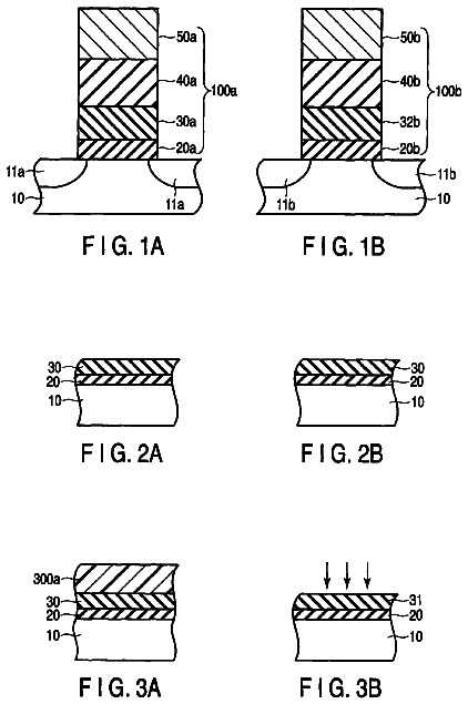
FIGS. 1A-1C are cross-sectional views showing a semiconductor device according to one embodiment of the present disclosure as viewed in the gate length direction, in the order in which the semiconductor device is fabricated.
FIGS. 2A-2C are cross-sectional views showing the semiconductor device of the embodiment of the present disclosure as viewed in the gate length direction, in the order in which the semiconductor device is fabricated.
FIGS. 3A-3C are cross-sectional views showing the semiconductor device of the embodiment of the present disclosure as viewed in the gate length direction, in the order in which the semiconductor device is fabricated.
FIGS. 4A-4C are cross-sectional views showing the semiconductor device of the embodiment of the present disclosure as viewed in the gate length direction, in the order in which the semiconductor device is fabricated.
FIGS. 5A-5C are cross-sectional views showing the semiconductor device of the embodiment of the present disclosure as viewed in the gate length direction, in the order in which the semiconductor device is fabricated.
FIG. 6 is a cross-sectional view showing a semiconductor device according to one embodiment of the present disclosure as viewed in the gate length direction.
FIG. 7 is a cross-sectional view showing a semiconductor device according to a variation of the embodiment of the present disclosure as viewed in the gate length direction.
FIGS. 8A-8C are cross-sectional views showing a conventional semiconductor device as viewed in the gate length direction, in the order in which the semiconductor device is fabricated.
FIGS. 9A-9C are cross-sectional views showing the conventional semiconductor device as viewed in the gate length direction, in the order in which the semiconductor device is fabricated.
FIGS. 10A-10C are cross-sectional views showing the conventional semiconductor device as viewed in the gate length direction, in the order in which the semiconductor device is fabricated.
Detailed description
A method for fabricating a semiconductor device according to one embodiment of the present disclosure will be described hereinafter with reference to FIGS. 1A-1C, 2A-2C, 3A-3C, 4A-4C, and 5A-5C. FIGS. 1A-5C are cross-sectional views showing the semiconductor device of the embodiment of the present disclosure as viewed in the gate length direction, in the order in which the semiconductor device is fabricated. In FIGS. 1A-5C, the term "first pMIS region" shown on the left side refers to a region where a first MIS transistor whose conductivity type is p-type is formed. The term "nMIS region" shown in the middle refers to a region where a second MIS transistor whose conductivity type is n-type is formed. The term "second pMIS region" shown on the right side refers to a region where a third MIS transistor whose conductivity type is p-type is formed. The term "first MIS transistor" refers to a MIS transistor having source/drain regions including a silicon compound layer. The first MIS transistor is used in, for example, a logic circuit or an internal circuit. The term "third MIS transistor" refers to a MIS transistor which does not include a silicide layer formed on source/drain regions. The third MIS transistor is used in, for example, an analog circuit or a peripheral circuit.
Initially, as shown in FIG. 1A, an isolation region 11 is selectively formed in an upper portion of a semiconductor substrate 10 made of, for example, p-type silicon, by, for example, a shallow trench isolation (STI) process. As a result, a first and a third active region 10a and 10c surrounded by the isolation region 11 are formed in the first and second pMIS regions of the semiconductor substrate 10. A second active region 10b surrounded by the isolation region 11 is formed in the nMIS region of the semiconductor substrate 10.
Next, an n-type impurity, such as phosphorus (P) etc., is implanted into the first and second pMIS regions of the semiconductor substrate 10 by an ion implantation process. On the other hand, a p-type impurity, such as boron (B) etc., is implanted into the nMIS region of the semiconductor substrate 10 by an ion implantation process. Thereafter, a thermal treatment is performed. As a result, a first and a second n-type well region 12a and 12c are formed in the first and second pMIS regions of the semiconductor substrate 10. A p-type well region 12b is formed in the nMIS region of the semiconductor substrate 10.
Next, a gate insulating film formation film made of, for example, a silicon oxide film having a thickness of 1.5 nm is deposited on the semiconductor substrate 10 by, for example, a chemical vapor deposition (CVD) process. Thereafter, a gate electrode formation film made of, for example, a polysilicon film having a thickness of 50 nm is deposited on the gate insulating film formation film by, for example, a CVD process. Thereafter, a protective insulating film formation film made of, for example, a silicon nitride film having a thickness of 30 nm is deposited on the gate electrode formation film by, for example, a CVD process.
Next, a resist pattern (not shown) is formed on the protective insulating film formation film by a lithography process, and thereafter, the protective insulating film formation film, the gate electrode formation film, and the gate insulating film formation film are successively patterned by a dry etching process using the resist pattern as a mask. As a result, a first gate electrode formation portion 15A including a first gate insulating film 13a, a first gate electrode 14a, and a first protective insulating film 15a is formed on the first active region 10a. A second gate electrode formation portion 15B including a second gate insulating film 13b, a second gate electrode 14b, and a second protective insulating film 15b is formed on the second active region 10b. A third gate electrode formation portion 15C including a third gate insulating film 13c, a third gate electrode 14c, and a third protective insulating film 15c is formed on the third active region 10c.
Next, an offset spacer film made of, for example, a silicon nitride film having a thickness of 5 nm is deposited by, for example, a CVD process, and thereafter, the offset spacer film is subjected to anisotropic dry etching. As a result, first, second, and third offset spacers 16a, 16b, and 16c whose cross-sections have an I-shape are formed on side surfaces of the first, second, and third gate electrode formation portions 15A, 15B, and 15C. Thereafter, a p-type impurity, such as B etc., is implanted into the first and third active regions 10a and 10c by an ion implantation process using the first and third gate electrode formation portions 15A and 15C and the first and third offset spacers 16a and 16c as a mask. As a result, first and second p-type extension injection regions 17a and 17c are formed in a self-aligning manner in the first and third active regions 10a and 10c laterally outside the first and third gate electrode formation portions 15A and 15C. On the other hand, an n-type impurity, such as arsenide (As) etc., is implanted into the second active region 10b by an ion implantation process using the second gate electrode formation portion 15B and the second offset spacers 16b as a mask. As a result, n-type extension injection regions 17b are formed in a self-aligning manner in the second active region 10b laterally outside the second gate electrode formation portion 15B.
Next, as shown in FIG. 1B, a first insulating film 18 made of, for example, a silicon oxide film having a thickness of 5 nm is deposited on an entire surface of the semiconductor substrate 10 by, for example, a CVD process. Thereafter, a second insulating film 19 made of, for example, a silicon nitride film having a thickness of 15 nm is deposited on the first insulating film 18 by, for example, a CVD process.
Next, as shown in FIG. 1C, a resist pattern Re which exposes the first pMIS region and covers the nMIS region and the second pMIS region is formed on the second insulating film 19 by a lithography process. Thereafter, the second insulating film 19 and the first insulating film 18 are successively subjected to anisotropic dry etching using the resist pattern Re as a mask. As a result, first inner sidewalls 18a which are made of the first insulating film and whose cross-sections have an L-shape are formed on side surfaces of the first gate electrode formation portion 15A with the first offset spacers 16a being interposed therebetween, and protective sidewalls 19a made of the second insulating film are formed on the first inner sidewalls 18a. On the other hand, a first and a second insulating film 18 and 19 which cover the second and third gate electrode formation portions 15B and 15C are left on the second and third active regions 10b and 10c.
In this case, the first inner sidewall 18a has a width W18a (largest width) of 20 nm (the sum of a thickness (5 nm) of the first insulating film 18 and a thickness (15 nm) of the second insulating film 19). By adjusting the thicknesses of the first and second insulating films 18 and 19, the width W18a of the first inner sidewall 18a can be adjusted. As used herein, the term "width" in relation to an inner sidewall whose cross-section has an L-shape (an inner sidewall having a first portion extending in a direction perpendicular to the main surface of the semiconductor substrate and a second portion extending in a direction parallel to the main surface of the semiconductor substrate) refers to a width (a width in a direction parallel to the main surface of the semiconductor substrate) of the second portion of the inner sidewall.
In this case, a thickness T19a of the protective sidewall 19a is the same as a thickness T19 of the second insulating film 19. Note that the thickness T19a of the protective sidewall 19a may be smaller than the thickness T19 of the second insulating film 19.
Next, as shown in FIG. 2A, the resist pattern Re is removed, and thereafter, the first active region 10a is subjected to, for example, dry etching using the protective sidewalls 19a and the second insulating film 19 as a mask. As a result, trenches 20 having a depth of, for example, 40 nm are formed in the first active region 10a laterally outside the protective sidewalls 19a.
Next, as shown in FIG. 2B, for example, a silane gas (SiH.sub.4 gas) and a germane gas (GeH.sub.4 gas) are supplied along with a p-type impurity gas, such as a diborane gas (B.sub.2H.sub.6 gas) etc., by, for example, a CVD process. As a result, a silicon compound layer 21 made of, for example, silicon germanium (SiGe) having a thickness of 80 nm is formed in the trenches 20. The silicon compound layer 21 causes a compressive stress in the gate length direction of the channel region in the first active region 10a. Because the silicon compound layer 21 is doped with a p-type impurity, such as B etc., the regions of the silicon compound layer 21 are p-type impurity-introduced regions.
In this case, the first and second insulating films 18 and 19 are successively formed to cover surfaces of the second and third active regions 10b and 10c. Therefore, a silicon compound layer is not formed on the second and third active regions 10b and 10c.
In this case, an upper surface of the first gate electrode 14a is covered by the first protective insulating film 15a. Therefore, a silicon compound layer is not formed on the first gate electrode 14a. The second and third protective insulating films 15b and 15c and the first and second insulating films 18 and 19 are successively formed to cover upper surfaces of the second and third gate electrodes 14b and 14c. Therefore, a silicon compound layer is not formed on the second and third gate electrodes 14b and 14c.
As described above, by adjusting the thicknesses of the first and second insulating films 18 and 19, the width W18a of the first inner sidewall 18a can be adjusted. Therefore, if the width W18a of the first inner sidewall 18a is adjusted to be narrow (as described later, for example, the width W18a is adjusted to be narrower than the widths W18b and 18c of the second and third inner sidewalls 18b and 18c), as shown in FIG. 2A the trench 20 can be formed in the first active region 10a closer to the channel region, and as shown in FIG. 2B the silicon compound layer 21 can be formed in the first active region 10a closer to the channel region.
Next, as shown in FIG. 2C, the protective sidewalls 19a (silicon nitride film), the second insulating film 19 (silicon nitride film), and the first protective insulating film 15a (silicon nitride film) are removed by an etching process (e.g., a wet etching process using hot phosphoric acid of 160.degree. C. as an etchant) having selectivity to a silicon oxide film (the first inner sidewalls 18a and the first insulating film 18). As a result, the first inner sidewalls 18a and an upper surface of the first gate electrode 14a are exposed in the first pMIS region, and the first insulating film 18 is exposed in the nMIS region and the second pMIS region.
In this case, because the first offset spacer 16a is made of a silicon nitride film, an upper portion of the first offset spacer 16a is removed.
In this case, upper surfaces of the second and third protective insulating films 15b and 15c (silicon nitride film) and upper ends of the second and third offset spacers 16b and 16c (silicon nitride film) are covered by the first insulating film 18 (silicon oxide film). Therefore, the second and third protective insulating films 15b and 15c and the second and third offset spacers 16b and 16c are not removed.
In this case, in the step of FIG. 1C, if the thickness T19a of the protective sidewall 19a is the same as the thickness T19 of the second insulating film 19, as shown in FIG. 2C the thickness T18a of the first inner sidewall 18a is the same as the thickness T18 of the first insulating film 18. Note that, in the step of FIG. 1C, if the thickness T19a of the protective sidewall 19a is smaller than the thickness T19 of the second insulating film 19, the first inner sidewall 18a is subjected to etching during a period of time from when the protective sidewall 19a having the smaller thickness T19a is removed to when the second insulating film 19 having the larger thickness T19 is removed. Therefore, the thickness T18a of the first inner sidewall 18a is smaller than the thickness T18 of the first insulating film 18.
The description continues in the full USPTO document.
 Lapsed, fee not paid7 drawings