Background art
The present invention relates to a defect inspection method and inspection device used to inspect microscopic defects present on a specimen surface and determine, output the kinds and sizes of defects.
At manufacturing lines for semiconductor substrates or thin-film substrates or the like, defects on the surface of a semiconductor substrate or thin-film substrate or the like are inspected to maintain/improve product yields. Known conventional techniques relating to defect inspection include those disclosed in, for example, Japanese Patent Application Publications JP-A-1997-304289 (Patent Document 1), JP-A-2006-201179 (Patent Document 2), and US Patent Application No. 2006/0256325 (Patent Document 3). In these conventional techniques, in order to detect microscopic defects, the surface of a specimen is irradiated with illumination light focused to a size of tens of micrometers (.mu.m). The scattered light from each defect is focused and detected, thereby inspecting defects with a size measuring between tens of nanometers (nm) and tens of micrometers (.mu.m) or larger. A stage holding the specimen (target substance) can be moved rotationally and translationally to helically scan the surface of the specimen and inspect the entire surface of the specimen.
Patent Documents 1 and 2 also describe techniques that detect high-angle emission components and low-angle emission components of the scattered light from defects to classify the defects based on the ratio between the two.
Patent Document 2 also describes a technique for calculating dimensions of a detected defect based on the intensity of the scattered light from the defect.
Patent Document 3 also describes a technique, for reducing thermal damage to the specimen, that controls power of illumination light, a scanning speed of the illumination spot, or a size of the illumination spot during the inspection of the intended surface. More specifically, the technique assumes that the thermal damage to the specimen is determined by a product of a density and irradiation time of the irradiating illumination power. In order to keep the product lower than a fixed value, the power of the illumination light, the scanning speed of the illumination spot, or the size of the illumination spot is changed in accordance with the radial position on the specimen under scanning.
In addition, U.S. Pat. No. 6,608,676 (Patent Document 4) discloses a technique for inspecting an entire surface of a specimen within a short time. A unidirectionally long gaussian beam is used to illuminate a broad region of the specimen and the entire illuminated region is detected at one time by a multi-pixel detector such as a CCD.
Furthermore, U.S. Pat. No. 7,385,688 (Patent Document 5) discloses a technique that uses a non-spherical lens or a diffractive optical element in off-axis illumination so that illumination light is shaped into an array of illumination spots on the surface of a target object.
Citation list
Patent Literature
Japanese Patent Laid-Open Number 1997-304289 Japanese Patent Laid-Open Number 2006-201179 US Publication Number 2006/0256325 U.S. Pat. No. 6,608,676 U.S. Pat. No. 7,385,688
Summary of invention
Technical Problem
The defect inspection used in manufacturing processes for semiconductors and/or the like is required to be able to detect microscopic defects, measure detected defect sizes with high accuracy, inspect the specimen non-destructively (or without transmuting the specimen), constantly obtain definite inspection results (counts, positions, sizes, and kinds of the detected defect) for one specimen, inspect a number specimens within a certain time, and more.
In the techniques described in Patent Documents 1, 2, 4, and 5, defects of sizes smaller than 20 nm, in particular, cannot be detected since the scattered light from the defect is very weak and is covered with noise of the scattered light on the surface of the specimen, noise of a detector, or noise of a detection circuit. If the illumination power is raised to avoid this, a temperature of the specimen would be significantly increased by the illumination light and the specimen may be thermally damaged. If the scanning speed for specimens is lowered to avoid thermal damage, a specimen area or total number of specimens inspectable within a fixed time would decrease. For these reasons, it has been difficult to detect microscopic defects at high speed while avoiding thermal damage.
In addition, when the specimen is scanned helically at a constant rotating speed, the moving speed of the illumination spot is minimal at the center of the specimen. Thus, significant thermal damage is applied to the central region of the specimen. In order to avoid this, for example, scanning may be performed while maintaining a constant linear velocity at a scanning position, or X-Y scanning may be conducted to thereby keep the irradiation time constant irrespective of the scanning position on the specimen. However in the former means, an infinite rotating speed is needed to inspect the central region of the specimen and the inspection of the central region is therefore substantially impossible. The latter means requires time for acceleration/deceleration of the stage in switching directions of main scanning and sub-scanning, and thus requires a long time to inspect whole-surface.
Further, the illumination light intensity distribution at the illumination spot is a gaussian distribution. Intensity of a scattered light signal from a defect, detected according to a relative position of the defect with respect to the illumination spot, thus changes and makes defect detection sensitivity variable and reduces defect size calculation accuracy.
On the other hand, the technique described in Patent Document 3 was intended to reduce thermal damage in the vicinity of the specimen center in comparison with other conventional techniques by changing the illumination power in proportion to the radial position on the specimen. Another aim of the technique was to suppress thermal damage in the vicinity of the specimen center at a level equivalent to that of other conventional techniques, while simultaneously improving defect detection sensitivity at the outer region of the specimen. However, assuming that thermal damage is proportional to the product of the irradiation power and the irradiation time causes the following problems.
Firstly, in the estimation of thermal damage, impacts of heat diffusion from the illumination spot are not considered. The thermal damage is prone to be overestimated especially at the central region of the specimen where the irradiation time is long. Thus, the illumination power at the central region of the specimen has been reduced to a level lower than required and defect detection sensitivity has decreased as a result.
Secondly, to avoid thermal damage to the entire surface of the specimen, it is necessary to define a certain level of the illumination power with respect to a standard where the central region of the specimen, that suffers the most thermal damage, is prevented from thermally damaged. However in rotational scanning, the scanning speed (linear velocity) is zero at the central region of the specimen. A theoretical irradiation time diverges to infinite and the thermal damage cannot be quantitatively estimated with the foregoing assumption, and thus the illumination power cannot be defined. Conversely, to guarantee that no thermal damage at the central region occurs, the illumination power needs to be zero so it is impossible to inspect the central region.
Thirdly, as described in Patent Document 3, changing the illumination power according to the radial position on the specimen makes peak values of the scattered light signal differ according to the position on the specimen, even for defects with same sizes. This may cause inconveniences: for example, defects in the outer circumferential region of the specimen may suffer signal saturation, or the peak value of a defect in the central region may decrease to an undetectable level. These inconveniences may result in the variability of defect detection sensitivity or the decrease in defect size calculation accuracy or the like.
Fourthly, as described in Patent Document 3, when a shape of the illumination spot is dynamically changed according to a radial position on the specimen, an illumination spot shape obtained depends on factors such as individual differences in the optical elements of an upstream illumination optical system or control accuracy. It is difficult to control the shape of the illumination spot accurately and also difficult to control the shapes of illumination spots equivalently between a plurality of devices.
Further, as described in Patent Document 5, when the technique that conducts scanning with an array of illumination spots is applied to helical scanning which is suitable for rapid inspection, a difference in curvature between scanning paths may make the scanning paths of the illumination spots overlap or reverse, depending on the radial position on the specimen. Inspection efficiency or an inspection area per unit time decreases as a result.
Further, as described in Patent Document 5, shaping an illumination spot using a non-spherical lens and a diffractive optical element may cause a slight shift in a position or angle, or a slight disturbance in an intensity distribution or wavefront of the light incident upon the non-spherical lens and the diffractive optical element. The outcoming shapes of the illumination spots would be variable and stable inspection results are difficult to obtain.
Solution to Problem
The present invention disclosed herein to solve the above problems is outlined below.
In a first aspect of the present invention the surface of a specimen is irradiated with illumination light having a substantially uniform illumination intensity distribution in a certain direction on the surface of the specimen. Next, the invention detects, of the light scattered from the surface of the specimen by the irradiation, a plurality of scattered-light components emitted in a plurality of directions different from each other, and obtains a plurality of corresponding scattered-light detection signals. After this, the invention determines existence of defects by processing at least one of the scattered-light detection signals, and further determines sizes of the defects by processing at least one of the scattered-light detection signals corresponding to the sections determined to be defective during the defect existence determination. Finally, the invention displays on a screen a positions of the detected defective sections on the specimen surface, and the defect sizes.
A second aspect of the present invention includes: an illumination light regulating step for conditioning illumination light that has been emitted from a light source to a beam of light having a desired quantity of light, position, beam diameter, and polarization state; an illumination intensity distribution control step for guiding the beam obtained in the illumination light regulating step to a specimen surface at a desired angle of incidence, and for controlling an illumination intensity distribution so that the illumination intensity distribution of light illuminating the surface of the specimen is substantially uniform in a certain direction on the specimen surface; a specimen scanning step for, at a position on the specimen surface where the specimen is irradiated with the illumination light in the illumination intensity distribution control step, moving the specimen in a direction substantially perpendicular to the direction in which the illumination intensity distribution is substantially uniform; a scattered-light detection step for detecting, of the scattered light emitted from the specimen surface in the specimen scanning step, a plurality of scattered-light components emitted in a plurality of directions different from each other, and for outputting a plurality of scattered-light detection signals corresponding to the detected scattered-light components; a defect determining step for determining existence of defects by processing at least one of the scattered-light detection signals obtained in the scattered-light detection step; a defect size determining step for determining sizes of the defects by processing at least one of the scattered-light detection signals corresponding to the sections determined to be defective in the defect existence determining step; and a display step for displaying positions of the detected defective sections on the specimen surface, and the defect sizes obtained in the defect size determining step.
A third aspect of the present invention includes: illumination light regulating means for regulating illumination light that has been emitted from a light source to a beam of light having a desired quantity of light, position, beam diameter, and polarization state; illumination intensity distribution control means for guiding the beam obtained by the illumination light regulating means to a specimen surface at a desired angle of incidence, and for controlling an illumination intensity distribution so that the illumination intensity distribution of light illuminating the surface of the specimen is substantially uniform in a certain direction on the specimen surface; specimen scanning means for, at a position on the specimen surface where the illumination intensity distribution control means irradiates the specimen with the illumination light, moving the specimen in a direction substantially perpendicular to the direction in which the illumination intensity distribution will be substantially uniform; scattered-light detection means for detecting, of scattered light emitted from the specimen surface by the illumination of the illumination light having the controlled illumination intensity distribution, a plurality of scattered-light components emitted in a plurality of directions different from each other, and for outputting a plurality of corresponding scattered-light detection signals corresponding to the detected scattered-light components; defect determining means for determining existence of defects by processing at least one of the scattered-light detection signals obtained in the scattered-light detection means; defect size determining means for determining sizes of the defects by processing at least one of the scattered-light detection signals corresponding to the sections determined to be defective in the defect existence determining means; and display means for displaying positions of the detected defective sections on the specimen surface, and the defect sizes obtained in the defect size determining means.
Advantageous Effects of Invention
The present invention scans the entire surface of a specimen within a short time, detects microscopic defects on the surface while reducing thermal damage to the specimen, calculates sizes of the detected defects accurately, and outputs stable inspection results.
These and other objects, features and advantages of the invention will be apparent from the following more particular description of preferred embodiments of the invention, as illustrated in the accompanying drawings.
Brief description of drawings
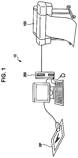
FIG. 1 is an overall schematic block diagram showing an embodiment of a defect inspection device according to the present invention;
FIG. 2 is a schematic showing a first example of an illumination intensity distribution shape implemented by an illumination unit according to the present invention;
FIG. 3 is a schematic showing a second example of an illumination intensity distribution shape implemented by the illumination unit according to the present invention;
FIG. 4 is a schematic showing a third example of an illumination intensity distribution shape implemented by the illumination unit according to the present invention;
FIG. 5 is a schematic showing a fourth example of an illumination intensity distribution shape implemented by the illumination unit according to the present invention;
FIG. 6 is a schematic showing a fifth example of an illumination intensity distribution shape implemented by the illumination unit according to the present invention;
FIG. 7 is a schematic showing a first example of an optical element included in an illumination intensity distribution controller according to the present invention;
FIG. 8 is a schematic showing a second example of an optical element included in the illumination intensity distribution controller according to the present invention;
FIG. 9 is a schematic showing a third example of an optical element included in the illumination intensity distribution controller according to the present invention;
FIG. 10 is a schematic showing a fourth example of an optical element included in the illumination intensity distribution controller according to the present invention;
FIG. 11 is a schematic showing a fifth example of an optical element included in the illumination intensity distribution controller according to the present invention;
FIG. 12 is a schematic showing a sixth example of an optical element included in the illumination intensity distribution controller according to the present invention;
FIG. 13 is a schematic showing a seventh example of an optical element included in the illumination intensity distribution controller according to the present invention;
FIG. 14 is a schematic showing a first example of means used to measure and control data relating to a state of illumination light in the illumination unit according to the present invention;
FIG. 15 is a schematic showing a second example of means used to measure and control the data relating to a state of illumination light in the illumination unit according to the present invention;
FIG. 16 is a schematic showing a first example of means used to reduce energy per pulse by means of optical path branching and combining in the illumination unit according to the present invention;
FIG. 17 shows energy-per-pulse reduction results based on optical path branching and combining;
FIG. 18 is a schematic showing a second example of means used to reduce energy per pulse by means of optical path branching and combining in the illumination unit according to the present invention;
FIG. 19 is a schematic illustration of a scanning direction and an illumination distribution shape on a specimen surface;
FIG. 20 is a schematic illustration showing a path of an illumination spot during scanning;
FIG. 21 is a side view that shows layout of detection units and a detection direction according to the present invention;
FIG. 22 is a top view that shows layout of low-angle detection units and a detection direction according to the present invention;
FIG. 23 is a top view that shows layout of high-angle detection units and a detection direction according to the present invention;
FIG. 24 is a schematic showing a first example of a detection unit configuration according to the present invention;
FIG. 25 is a schematic showing a second example of a detection unit configuration according to the present invention;
FIG. 26 is a schematic showing an analog processing unit configuration according to the present invention;
FIG. 27 is a schematic showing a digital processing unit configuration according to the present invention;
FIG. 28 is a schematic representing a relationship between length of an illumination spot and an increase in specimen surface temperature, in the present invention;
FIG. 29 is a schematic representing a relationship between the length of an illumination spot and allowable illumination power, in the present invention;
FIG. 30 is a schematic representing a relationship between an illumination light irradiation time and an increase in specimen surface temperature, in the present invention;
FIG. 31 is a schematic representing a relationship between an illumination light irradiation time and allowable illumination power, in the present invention;
FIG. 32 is a flow diagram of illumination state control in an illumination unit according to the present invention;
FIG. 33 is a schematic showing an eighth example of an optical element included in the illumination intensity distribution controller according to the present invention;
FIG. 34 is a diagram that shows illumination intensity distribution intermediate image and illumination intensity distribution states obtained on the specimen surface by the illumination intensity distribution controller in the eighth example according to the present invention;
FIG. 35 is a schematic showing a ninth example of an optical element included in the illumination intensity distribution controller according to the present invention;
FIG. 36 is a schematic showing a tenth example of an optical element included in the illumination intensity distribution controller according to the present invention; and
FIG. 37 is a schematic showing an eleventh example of an optical element included in the illumination intensity distribution controller according to the present invention.
Description of embodiments
A schematic exemplary configuration of a defect inspection device according to an embodiment of the present invention is described below referring FIG. 1. The defect inspection device includes an illumination unit 101, a detection unit 102, a stage 103 on which a specimen W can be mounted, a signal processing unit 105, a control unit 53, a display unit 54, and an input unit 55, as appropriate. The illumination unit 101 includes a laser light source 2, an attenuator 3, an exit beam regulator 4, a beam expander 5, a polarization controller 6, and an illumination intensity distribution controller 7, as appropriate. A laser light beam that has been emitted from the laser light source 2 is controlled to desired beam intensity by the attenuator 3, adjusted to a desired beam position and a beam traveling direction by the exit beam regulator 4, and is controlled to a desired beam diameter by the beam expander 5. The beam is next controlled to a desired polarization state by the polarization controller 6, then controlled to a desired intensity distribution by the illumination intensity distribution controller 7, and then illuminated at a target region of the wafer W.
An angle of incidence of the illumination light with respect to the specimen surface is determined by a position and angle of a reflecting mirror of the exit beam regulator 4, disposed in an optical path of the illumination unit 101. The incident angle of the illumination light is set to an angle appropriate for detecting microscopic defects. As the incident angle of the illumination light increases, that is, an illumination elevation (an angle between the specimen surface and an illumination optical axis) decreases, the scattered light from microscopic irregularities on the specimen surface which acts as noise for the scattered light from microscopic contamination on the specimen surface (haze) becomes weaker. Thus, small incident angles of the illumination light are suitable for detecting microscopic defects. Accordingly, if the scattered light from the microscopic irregularities on the specimen surface obstructs the detection of microscopic defects, the incident angle of the illumination light is preferably set to 75 degrees or larger (the elevation is preferably 15 degrees or smaller). On the other hand, in off-axis illumination, as an incident angle of the illumination light is smaller, an absolute quantity of the scattered light from microscopic contamination gets greater. Therefore if a shortage of the amount of scattered light scattered from a defect obstructs the detection of the defect, the incident angle of the illumination light is preferably set to 60 to 75 degrees (the elevation preferably is between 15 and 30 degrees). In addition, in off-axis illumination, the polarization controller 6 of the illumination unit 101 makes the illumination light P-polarized. This increases the amount of light scattered from the defect on the specimen surface in comparison with the amount of light with different polarization.
In addition, as shown in FIG. 1, the mirror 21 and other appropriate mirrors are disposed in the optical path of the illumination unit 101 as required. The optical path of the illumination light changes so that the light is irradiated from a direction substantially perpendicular to the specimen surface (vertical illumination). During the irradiation, the illumination intensity distribution on the specimen surface is controlled by an illumination intensity distribution controller 7v, as with the case of off-axis illumination. When a beam splitter is inserted at the same position as that of the mirror 21 to obtain scattered light from off-axis illumination light and a concaved defect on the specimen (polishing scratches or crystalline defects in a crystal material), vertical illumination in which light enters the specimen surface at a substantially vertical angle is suitable. An illumination intensity distribution monitor 24 shown in FIG. 1 is described in detail later.
For the detection of microscopic defects near the specimen surface, the laser light source 2 is such that has high power of 2 W or more and oscillates ultraviolet or vacuum-ultraviolet laser beams of a short wavelength (355 nm or less) to minimize penetration into the specimen. The diameter of an exit beam is about 1 mm. For the detection of defects inside the specimen, the laser light source 2 is such that oscillates visible or infrared laser beams of a wavelength at which the light relatively easily penetrates into the specimen.
The attenuator 3 includes a first polarizer, a half-wave plate rotatable around the optical axis of the illumination light, and a second polarizer, as appropriate. Light that has entered the attenuator 3 is converted into a linearly polarized light by the first polarizer, next is turned to an optional polarization direction according to a slow-axis azimuth of the half-wave plate, and then passes through the second polarizer. The intensity of the light is reduced at an optional ratio by controlling the azimuth of the half-wave plate. The first polarizer is not needed if the light entering the attenuator 3 has a sufficiently high degree of linear polarization. The attenuator 3 is to have been calibrated the relationship between an input signal level and a light reduction rate beforehand. The attenuator 3 may be an ND filter having a gradation density distribution.
The exit beam regulator 4 includes plural reflecting mirrors. While the regulator 4 in the present example includes two reflecting mirrors, the number of reflecting mirrors is not limited and the regulator 4 may have three or more reflecting mirrors when needed. Here, an imaginary three-dimensional rectangular coordinate system (XYZ coordinates) is defined, and the light incident upon the reflecting mirrors is assumed to travel in a +X direction. A first reflecting mirror is set to deflect the incident light in a +Y direction (incidence/reflection in an XY plane), and a second reflecting mirror is set to deflect the incident light that has been reflected by the first reflecting mirror in a +Z direction (incidence/reflection in a YZ plane). At these reflecting mirrors, the position and traveling direction (angle) of the light emitted from the exit beam regulator 4 are controlled by parallel movement and tilt angle adjustment. The incident/reflection plane (XY plane) of the first reflecting mirror and the incident/reflection plane (YZ plane) of the second reflecting mirror are disposed so as to cross at right angles as described above. Therefore, positions and angles of the light emitted from the exit beam regulator 4 (travels in a +Z direction) in XZ-plane and in YZ-plane can be controlled independently.
The beam expander 5 includes at least two lens groups and has a function that enlarges a diameter of incoming parallel beams of light. The beam expander 5 may be of a Galilean type including a combination of a concave lens and a convex lens for example. The beam expander 5 is placed on a translation stage which is movable along two or more axes and its position can be adjusted to align a predetermined beam position and the center of the expander. A tilt angle adjusting function for adjusting the angle of the entire beam expander 5 is also included to align an optical axis of the beam expander 5 with a predetermined beam optical axis. The enlargement ratio of the beam diameter can be controlled by adjusting the interval between the lenses (zoom mechanism). If the beams entering the beam expander 5 are not parallel, the enlargement in diameter and collimation (quasi-parallelization) of the beams are conducted at the same time during the adjustment of the lens interval. The collimation of the beams may be conducted by providing a collimating lens independent of the beam expander 5 upstream of the expander. The enlargement rate for the beam diameter of the beam expander 5 is about 5 to 10 times: for example, a beam emitted from the light source of a diameter about 1 mm would be enlarged to about 5 to 10 mm.
The polarization controller 6 includes a half-wave plate and a quarter-wave plate, and controls the illumination light to any polarization state. Monitors 22 and 23 measures, in a midway of the optical path of the illumination unit 101, data on the state of the light incident upon the beam expander 5 and the state of the light incident upon the illumination intensity distribution controller 7.
FIGS. 2 to 6 show schematic diagrams of relationships in position between the optical axis 120 and an intensity distribution shape of the illumination light guided to the specimen surface by the illumination unit 101. Constituent elements of the illumination unit 101 shown in FIGS. 2 to 6 are part of the illumination unit configuration, and the exit beam regulator 4, the mirror 21, the beam monitors 22, 23, and other elements are omitted from the figures. A schematic cross-sectional view of an incidence plane of off-axis illumination light (the plane including the illumination optical axis and a specimen surface normal) is shown in FIG. 2. The off-axis illumination light is inclined to the specimen surface in the incident plane. The illumination unit 101 forms a substantially uniform illumination intensity distribution in the incidence plane. Length of a portion uniform in illumination intensity is about 100 .mu.m to 1 mm so as to inspect a wide area within a unit time. A schematic cross-sectional view of the plane which includes the specimen surface normal and is perpendicular to the incident plane of off-axis illumination is shown in FIG. 3. In this plane, the illumination intensity distribution on the specimen surface is such that a peripheral area has a weak intensity relative to that of the central area. More specifically, this illumination intensity distribution is a gaussian distribution that reflects the intensity distribution of the light entering the illumination intensity distribution controller 7, or an intensity distribution that resembles a first kind/first-order Bessel function or a sinc function that reflects an aperture shape of the illumination intensity distribution controller 7. Length of the illumination intensity distribution in the incident plane (length of a region having at least 13.5% of maximum illumination intensity) ranges between about 5 .mu.m and 20 .mu.m. This is smaller than the length of the above portion uniform in illumination intensity in the incident plane so as to reduce haze arising from the specimen surface. The illumination intensity distribution controller 7 includes optical elements such as a non-spherical lens, diffractive optical element, cylindrical lens array, and light pipe, which are described later. The optical elements constituting the illumination intensity distribution controller 7 are placed perpendicularly to the illumination optical axis, as shown in FIGS. 2, 3.
The illumination intensity distribution controller 7 includes an optical element that acts upon the intensity distribution and a phase distribution of the light entering the controller 7. One of such optical elements constituting the illumination intensity distribution controller 7 is a diffractive optical element (DOE) 71 shown in FIG. 7. The diffractive optical element 71 is of a substrate that is made from a material which transmits the incident light and whose surface is corrugated with micro patterns of a size equivalent to or smaller than a wavelength of light. As the material that transmits incident light, fused quartz is used for ultraviolet light. The diffractive optical element 71 is preferably coated with an anti-reflection film to suppress attenuation of the light passing through the diffractive optical element 71. Lithography is used to form the micro corrugation. The light that has passed through the beam expander 5 and has been quasi-paralleled is further passed through the diffractive optical element 71, thereby forming an illumination intensity distribution corresponding to the corrugation of the diffractive optical element 71 on the specimen surface. The corrugated surface shape of the diffractive optical element 71 is designed and formed based on calculations using Fourier optics theory, so that the illumination intensity distribution formed on the specimen surface will be a long uniform distribution in the incident plane. The optical element of the illumination intensity distribution controller 7 includes a translational control mechanism and a rotational control mechanism both having two or more axes. These mechanisms enable the position and the angle of the element with respect to the optical axis of the incident light to be adjustable. A focus adjustment mechanism for adjusting focus by moving the element in the optical axis direction is also provided.
The illumination light state-measuring means in the illumination unit 101 is described below using FIG. 14. The beam monitor 22 measures and outputs data corresponding to the position and angle (traveling direction) of the illumination light which has passed through the exit beam regulator 4. The beam monitor 23 measures and outputs data corresponding to the position and wavefront of the illumination light entering the illumination intensity distribution controller 7.
The position measurement of the illumination light at the beam monitor 22 is conducted by measuring the center of gravity of the illumination light intensity. Specifically, a position-sensitive detector (PSD) or an image sensor such as a CCD sensor or CMOS sensor is among the position-measuring means. The angle measurement of the illumination light is conducted by the beam monitor 22 by using a beam position sensor or an image sensor placed at a position more remote from the light source than the above position-measuring means. The position and angle of the illumination light measured by the beam monitor 22 are input to the control unit 53 and then displayed on the display unit 54. When the position or angle of the illumination light deviates from a predetermined position or angle, the exit beam regulator 4 controls the light back to the predetermined position or angle.
Position measurement of the illumination light by the beam monitor 23 is conducted by means substantially same with the position-measuring means of the beam monitor 22. However, since the beam diameter is expanded to several millimeters or more at the measurement position of the beam monitor 23, the measurement position is projected in reduced size on a light-receiving surface of a detection element of the position-measuring means (a position-sensitive detector for instance), prior to the measurement. Wavefront measurement of the illumination light by the beam monitor 23 is conducted to measure a parallelism level of the light entering the illumination intensity distribution controller 7. The illumination light is measured with a shearing interferometer or a Shack-Hartmann wavefront sensor. A shearing interferometer is such that has an optical glass plate with both sides planarly polished and thickness of about several millimeters, and the optical glass is inserted in the illumination optical path obliquely inclined. Light reflected from an upper surface and a lower surface is projected on a screen and the pattern of interference fringes is observed to thereby measure a divergence/convergence state of the illumination light. The SPU-25, manufactured by Sigma Koki Co., Ltd., can be named as an example of shearing interferometers. The illumination light divergent/convergent state can be automatically measured by disposing a CCD sensor or an image sensor such as a CMOS sensor at a screen position. A Shack-Hartmann wavefront sensor employs a micro lens array to divide a wavefront, projects the divided wavefronts on an image sensor such as a CCD sensor, and measures inclinations of each wavefront from variations in the projection position. Compared with shearing interferometers, Shack-Hartmann wavefront sensors can conduct detailed wavefront measurements: for example, can measure partial disturbances in wavefront. When the light entering the illumination intensity distribution controller 7 is found through wavefront measurement to be not quasi-parallel light and diverged or converged, the illumination light can be neared to quasi-paralleled light by moving the lenses of the beam expander 5, in the preceding stage of the controller 7, along the optical axis. When, through the wavefront measurement, the light entering the illumination intensity distribution controller 7 is found to be partially inclined, the wavefront can be brought more planar, in other words, the illumination light can be neared to quasi-paralleled light in the following way. As shown in FIG. 15, a spatial light phase modulator 26 is inserted into the preceding stage of the illumination intensity distribution controller 7, and an appropriate phase difference is imparted to each position of a cross-section of the light beam so that the wavefront will be more planar. The above wavefront accuracy measuring/controlling means suppresses wavefront accuracy of the light (a departure from a predetermined wavefront (design value)) entering the illumination intensity distribution controller 7 to .lamda./10 rms or less.
The illumination intensity distribution on the specimen surface conditioned by the illumination intensity distribution controller 7 is measured by the illumination intensity distribution monitor 24. When vertical illumination is employed, as shown in FIG. 1, the illumination intensity distribution on the specimen surface conditioned by the illumination intensity distribution controller 7v is measured by the illumination intensity distribution monitor 24 as well. The illumination intensity distribution monitor 24 detects the specimen surface as an image by imaging the surface on an image sensor such as a CCD sensor or a CMOS sensor via lenses. The image of the illumination intensity distribution that is detected by the illumination intensity distribution monitor 24 is processed by the control unit 53 to calculate factors such as the center of gravity of intensity, maximum intensity, maximum intensity position, width and length of the illumination intensity distribution (i.e., width and length of the illumination intensity distribution region of which intensity is equal to or larger than a predetermined intensity level or of which intensity ratio is equal to or larger than a predetermined ratio with respect to the maximum intensity level). Calculation results are displayed at the display unit 54 along with a profile shape, a cross-sectional waveform, etc. of the illumination intensity distribution.
The description continues in the full USPTO document.
 Lapsed, fee not paid14 drawings